Today we will look at the remote control unit for the Robotic Toy Car – Part 6. The project is close to being completed, and as such, there are quite a lot of final things that need to be taken care of.
One of these will definitely be the final coding, which I will release in the final part of the project, so with that in mind, let us take a look at the remote control unit.
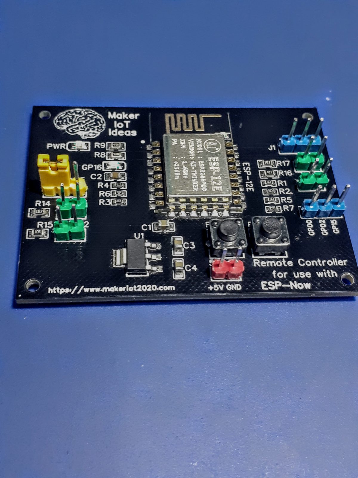
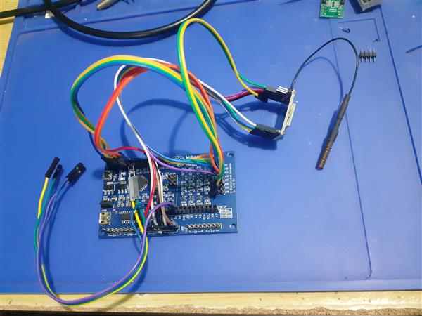
Remote Control Unit, designed to be used with ESP-Now
I have decided to do something completely different from standard remote control units, being that I will use ESP-Now, a protocol developed by Espressif. ESP-Now runs on the Wifi hardware of the ESP8266 or ESP32 and is basically a peer-to-peer protocol, that does not require Wifi but can co-exist with it on the same device. Outdoors, ESP-Now has a range of about 100m, which should work very well for my intended use.
The Remote control, as designed, will have 4 dedicated buttons: forward, reverse, left and right, divided into two groups to make two-handed control easier, similar to a standard game controller. No input on either of the two groups will result in stopping the vehicle, in the case of forwards and backwards, and centring the steering, in the case of the left-right axis.
a 3D Rendered Image of the PCB, motion axis on SW1 and SW2, steering axis on SW3 and SW4
As I always try to make my designs somewhat reusable for other purposes, I have also broken out most of the unused GPIO pins to header pins, with also adding a jumper on GPIO16 to make deep-sleep wakeup mode possible., You can also re-use the switch pins for other purposes, just remember to first remove the 10k pull-up resistors at R14, R15, R16, and R17…
GPIO16 can be reused as well, just remove the jumper, but remember that it is pulled up through a LED and a 470ohm resistor…
There is no USB-to-serial converter onboard, I have been having quite a lot of headaches with them over the last few months, with almost all CH340G chips that I have purchased, being fake, or dead-on arrivals that don’t work… Sending them back to the suppliers, unfortunately, results in unpleasantries, because even placing them in verified working circuits, still proves them to be not working… This is however not an issue, as it is quite easy to upload the board with an external adapter.
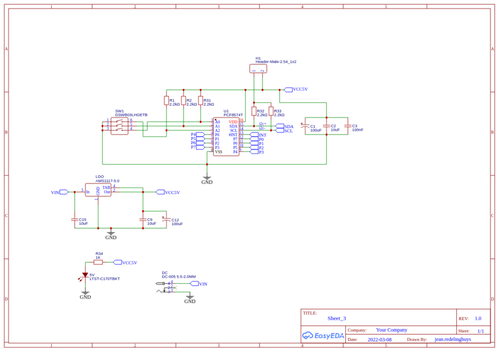
The Schematic
Schematic Diagram
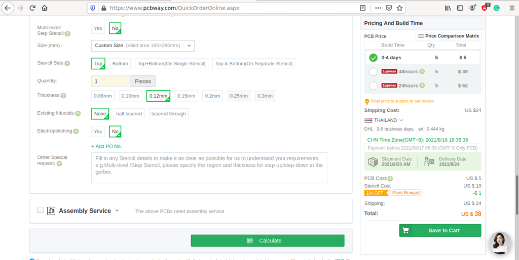
Manufacturing the PCB
Over the past eight years, PCBWay has continuously upgraded their MANUFACTURING plants and equipment to meet higher quality requirements, and now THEY also provide OEM services to build your products from ideas to mass production and access to the market.
The PCB for this project has been manufactured at PCBWay. Please consider supporting them if you would like your own copy of this PCB, or if you have any PCB of your own that you need to have manufactured.
If you would like to have PCBWAY manufacture one of your own, designs, or even this particular PCB, you need to do the following… 1) Click on this link 2) Create an account if you have not already got one of your own. If you use the link above, you will also instantly receive a $5USD coupon, which you can use on your first or any other order later. (Disclaimer: I will earn a small referral fee from PCBWay. This referral fee will not affect the cost of your order, nor will you pay any part thereof.) 3) Once you have gone to their website, and created an account, or login with your existing account,
4) Click on PCB Instant Quote
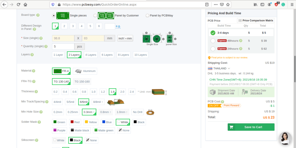
5) If you do not have any very special requirements for your PCB, click on Quick-order PCB
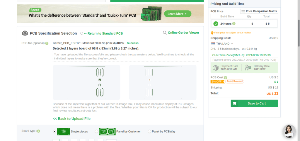
6) Click on Add Gerber File, and select your Gerber file(s) from your computer. Most of your PCB details will now be automatically selected, leaving you to only select the solder mask and silk-screen colour, as well as to remove the order number or not. You can of course fine-tune everything exactly as you want as well.
7) You can also select whether you want an SMD stencil, or have the board assembled after manufacturing. Please note that the assembly service, as well as the cost of your components, ARE NOT included in the initial quoted price. ( The quote will update depending on what options you select ).
8) When you are happy with the options that you have selected, you can click on the Save to Cart Button. From here on, you can go to the top of the screen, click on Cart, make any payment(s) or use any coupons that you have in your account.
Then just sit back and wait for your new PCB to be delivered to your door via the shipping company that you have selected during checkout.
In this part of the series, Robotic Toy Car – Part 4, We will add some custom side-panels to the project. While the original toy did come with some laser cut aluminum side panels, I decided to replace them with PCB versions, with even more flashing lights (yes, this thing is turning into a “Christmas tree” , but that is what the eventual owner wanted… )
These side-panels will not be programmable. They will simply be operated from a standard 555 timer and a couple of other components, to give a flash time of about one second on and off each…
It is also an excellent project to showcase the capabilities of PCBWay, in dealing with a “rather difficult” PCB to manufacture. As you may know by now, I use PCBWay‘s services quite extensively, and I also only design my PCB’s with EasyEDA. EasyEDA is however quite limited in some aspects, and as far as myself, making panels of different designs on one PCB with complex shapes is not something that I do every day…
Let us take a look at what had to be done, and how well it was manufactured…
The PCB Layout
What we have here, is basically two mirrored side-panels ( as far as the visible “outside” is concerned anyway ) That consists of 6 led’s per side that will flash alternatively. On the “inside” we have a 555 timer chip, with some resistors and capacitors, as well as transistors that does the switching.
The Schematic
The difficulty of this PCB is definitely in the manufacturing. I was however pleasantly surprised with the excellent work that was done by PCBWay. Their Engineering staff did contact me early on in the order, with a suggested plan to manufacture, and once I approved that, they very quickly went on to production. My initial concern was that they suggested “mouse-bites” which we all know can sometimes come out a bit strange…
Completed PCB in packaging..
I was however extremely pleased when the above parcel arrived… They added side rails, and the “mouse-bytes” were super tiny.
After assembly ( not cleaned up yet )After Assembly ( not cleaned up yet )Installed on the toy car body
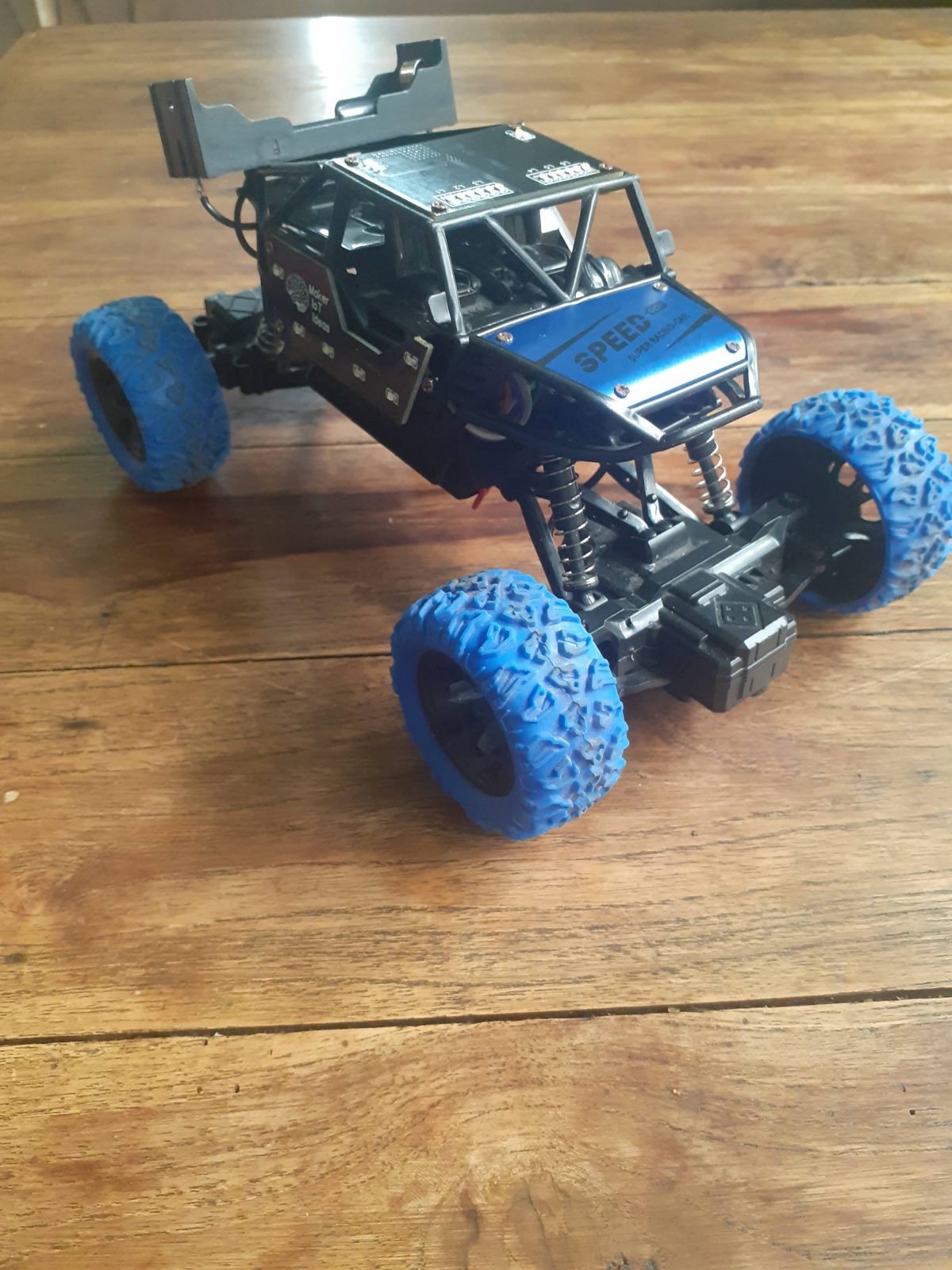
The “almost completed ” Robotic Toy Car
With the completion of the side-panels, it was also time to start work on the power wiring and other essential components of the project, which will get their own detailed post in a few days.
the “almost completed” project
Some details on the construction: The toy originally came with a single 500mA 14500 cell, which unfortunately stopped working very soon after only a few uses… This was however one of the reasons why the entire project happened in the first place, so no complaints there.
I decided to replace it with a 18560 cell with a capacity of about 1900mA. This cell is much bigger however, and I had to think of where to place it. I decided to put it on the roof, sort of emulating a “spoiler”.
Some of the next parts of the project will be the remote control unit, which will basically be an ESP8266 running ESP-Now protocol, as well as a decent battery charging and power distribution circuit, that will protect the Lipo cell from over charging and discharging, as well as provide sufficient power for all the added electronics in the toy car.
“But you said it was Robotic, so why have a remote control?”
The initial plan for the project did indeed say robotic, but it is also designed to be a learning platform, especially to teach coding. With that in mind, it is definitely better to keep things simple for now, and add sensors and more capabilities later on, especially as I am actually planning to replace the main MCU board with a more powerful ESP32 in a next version anyway.
The car body is also extremely cramped, and does not have any space for mounting sensors at all. I plan to remedy that by designing and 3d-printing a whole new custom body shell later… providing that my young friend actually stays interested enough to learn the coding… If he doesn’t, he will as least have a very interesting looking custom remote controlled toy car.
Manufacturing the PCB
The PCB for this project is currently on its way from China, after having been manufactured at PCBWay. Please consider supporting them if you would like your own copy of this PCB, or if you have any PCB of your own that you need to be manufactured.
If you would like to have PCBWAY manufacture one of your own, designs, or even this particular PCB, you need to do the following… 1) Click on this link 2) Create an account if you have not already got one of your own. If you use the link above, you will also instantly receive a $5USD coupon, which you can use on your first or any other order later. (Disclaimer: I will earn a small referral fee from PCBWay. This referral fee will not affect the cost of your order, nor will you pay any part thereof.) 3) Once you have gone to their website, and created an account, or login with your existing account,
4) Click on PCB Instant Quote
5) If you do not have any very special requirements for your PCB, click on Quick-order PCB
6) Click on Add Gerber File, and select your Gerber file(s) from your computer. Most of your PCB details will now be automatically selected, leaving you to only select the solder mask and silk-screen colour, as well as to remove the order number or not. You can of course fine-tune everything exactly as you want as well.
7) You can also select whether you want an SMD stencil, or have the board assembled after manufacturing. Please note that the assembly service, as well as the cost of your components, ARE NOT included in the initial quoted price. ( The quote will update depending on what options you select ).
8) When you are happy with the options that you have selected, you can click on the Save to Cart Button. From here on, you can go to the top of the screen, click on Cart, make any payment(s) or use any coupons that you have in your account.
Then just sit back and wait for your new PCB to be delivered to your door via the shipping company that you have selected during checkout.
In our last project, we started working on repurposing an old toy car. In this part, Robot Toy Car – The next steps, we will take a look at the controller board for this project and discuss some of the problems that we have encountered up to now. Most of the various components for this project are still in the prototype stage, but It is quite important to get them tested to verify the final designs.
There are quite a few unique challenges in a project like this, which looks quite easy to solve but turn out to become quite challenging to get working just right in practice…
One of the most important, as well as the most frustrating part, turned out to be the H-Bridge Motor controller. The first prototype of this was introduced in the first part of this project. While functional on paper, as well as working quite well in real life, (when tested with an Arduino, as well as manually), It performs extremely poorly when used with the actual controller for this project, an ESP8266 12-E…
What could the reason be? How will I fix it…? The answers to that will be provided in a follow-up post. For now, let us take a look at the controller.
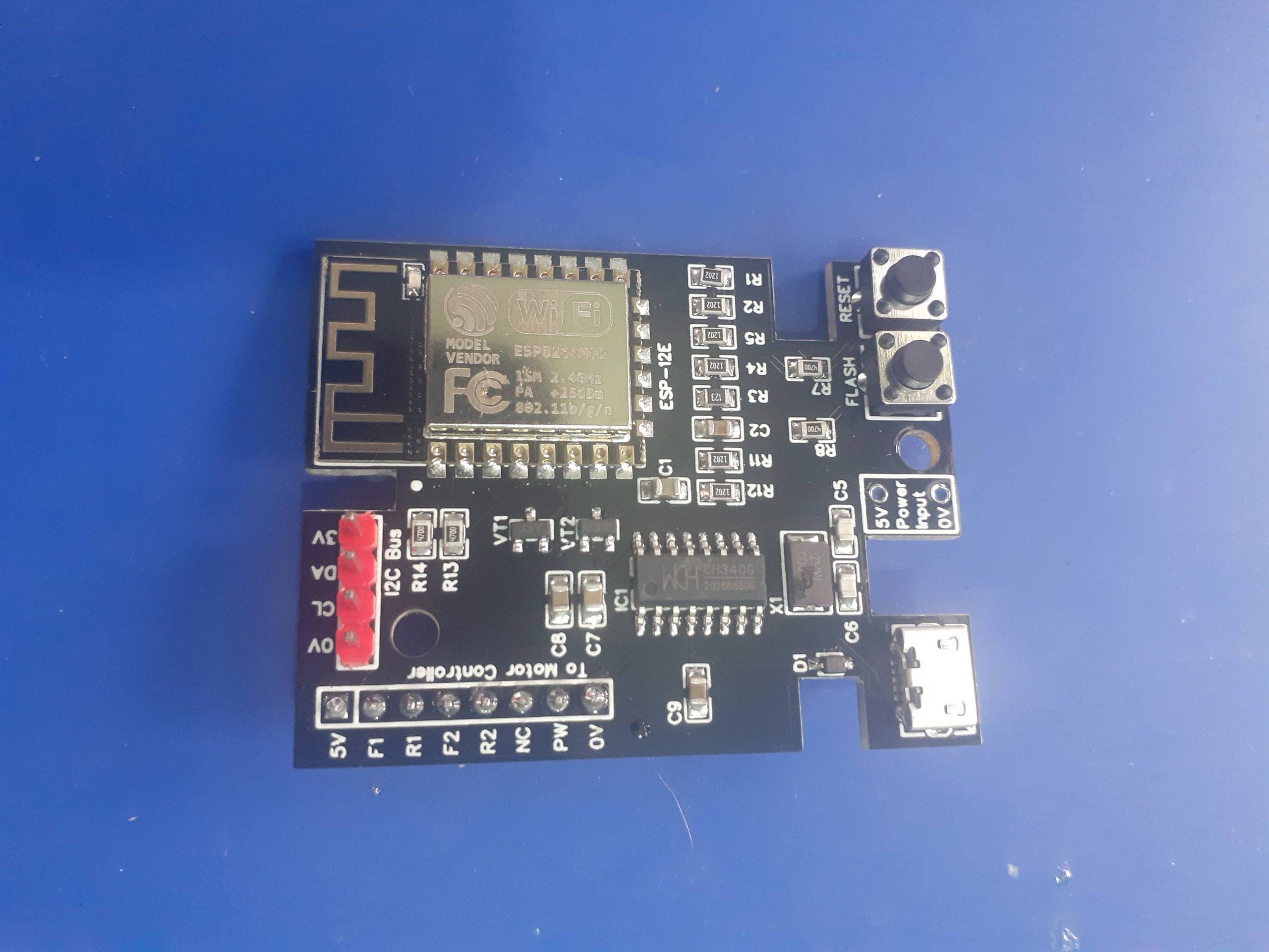
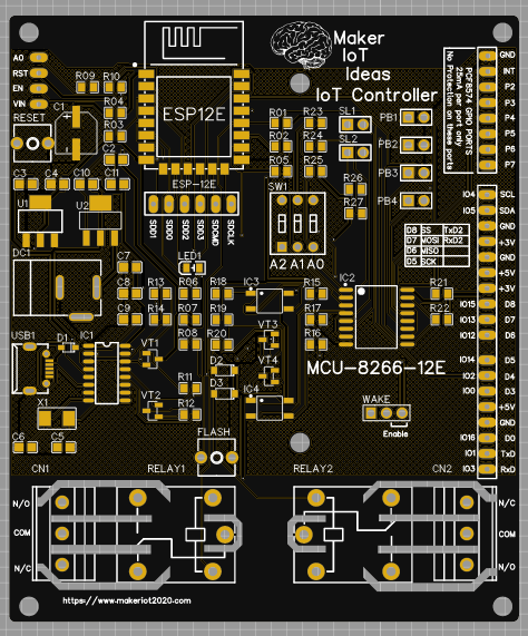
The unassembled ESP-8266 Controller board, straight from the factoryThe Assembled ESP-8266 Controller board.
The Controller Board, details
Space inside the toy car is at a premium, so from the start, it was important to design a PCB that was small enough to fit, while also taking into consideration functionality, as well as all additional add-on components to ultimately be fitted to the project.
With this in mind, I have decided on the ESP-8266, which, while bigger than an Atmega328, does offer a few additional features, like WiFi, and ESP-Now, which will greatly help in controlling and even updating firmware OTA. The ESP-8266 does however also have a few serious flaws in this design, like limited useable GPIO pins, a 3.3v working voltage requirement, and quite high operating current requirements.
As the toy will likely not be used continuously, as well as the fact that it will run on batteries, which, can be replaced or recharged, I did not worry too much about the power issue. As far as the limited GPIO, that is where I2C comes in… It is quite easy to expand the GPIO with an IO Expander or two…
My main problem came in the form of the CH340G USB-to-UART converter chip. It seems like there must be quite a lot of counterfeit versions of these around, as none of the chips that I purchased, from many different suppliers, actually functioned, with the best one actually providing a USB port, but, when investigating with a logic analyser, the Rx and Tx lines of the UART, generating garbage…
Replacing it with a known working chip from a NodeMCU V1 board, magically solved the problem, verifying the PCB circuit as correct and working, and also proving that the purchased chips are definitely fake!
This was easily repaired by temporarily soldering jumper cables to the Rx and Tx lines on the ESP-8266, and using an external UART-to-USB converter to upload the initial sketch to the device. Future updates will be OTA, so not a problem in the long run anyway.
Controller Schematic
The controller schematic, above, is basically a rearranged stock NodeMCU v1 circuit, with the only difference being that only specific pins were broken out onto header pins. These will be used for controlling the two H-Bridges, and provide PWM as well as access to the I2C bus.
Software
Due to the fact that this controller is still definitely considered a prototype, my main focus is definitely on getting the control software sorted out first. That way, at least in my opinion, I can then focus on hardware issues responding to verified software inputs, without having to do both at the same time.
As mentioned before, I require OTA capability to upload new firmware to the device, so my starting point was the BasicOTA sketch provided with the Arduino IDE. This sketch was modified to perform some additional functionality, such as controlling the H-Bridges, PWM as well as a roof-mounted “status panel” with LED’s that also doubles as a visual display, to give a bit of colour to the project.
The “status panel” will be shown in a future post, however, with the only mention of it here being that it is I2C controlled, and based on a PCF8574.
The BasicOTA sketch is listed below.
#include <ESP8266WiFi.h>
#include <ESP8266mDNS.h>
#include <WiFiUdp.h>
#include <ArduinoOTA.h>

#ifndef STASSID
#define STASSID "your-ssid"
#define STAPSK  "your-password"
#endif

const char* ssid = STASSID;
const char* password = STAPSK;

void setup() {
  Serial.begin(115200);
  Serial.println("Booting");
  WiFi.mode(WIFI_STA);
  WiFi.begin(ssid, password);
  while (WiFi.waitForConnectResult() != WL_CONNECTED) {
    Serial.println("Connection Failed! Rebooting...");
    delay(5000);
    ESP.restart();
  }

  // Port defaults to 8266
  // ArduinoOTA.setPort(8266);

  // Hostname defaults to esp8266-[ChipID]
  // ArduinoOTA.setHostname("myesp8266");

  // No authentication by default
  // ArduinoOTA.setPassword("admin");

  // Password can be set with it's md5 value as well
  // MD5(admin) = 21232f297a57a5a743894a0e4a801fc3
  // ArduinoOTA.setPasswordHash("21232f297a57a5a743894a0e4a801fc3");

  ArduinoOTA.onStart([]() {
    String type;
    if (ArduinoOTA.getCommand() == U_FLASH) {
      type = "sketch";
    } else { // U_FS
      type = "filesystem";
    }

    // NOTE: if updating FS this would be the place to unmount FS using FS.end()
    Serial.println("Start updating " + type);
  });
  ArduinoOTA.onEnd([]() {
    Serial.println("\nEnd");
  });
  ArduinoOTA.onProgress([](unsigned int progress, unsigned int total) {
    Serial.printf("Progress: %u%%\r", (progress / (total / 100)));
  });
  ArduinoOTA.onError([](ota_error_t error) {
    Serial.printf("Error[%u]: ", error);
    if (error == OTA_AUTH_ERROR) {
      Serial.println("Auth Failed");
    } else if (error == OTA_BEGIN_ERROR) {
      Serial.println("Begin Failed");
    } else if (error == OTA_CONNECT_ERROR) {
      Serial.println("Connect Failed");
    } else if (error == OTA_RECEIVE_ERROR) {
      Serial.println("Receive Failed");
    } else if (error == OTA_END_ERROR) {
      Serial.println("End Failed");
    }
  });
  ArduinoOTA.begin();
  Serial.println("Ready");
  Serial.print("IP address: ");
  Serial.println(WiFi.localIP());
}

void loop() {
  ArduinoOTA.handle();
}
Controlling the Toy Car Robot
Controlling the Toy Car is a complicated question, with many ideas jumping into my mind, only to be pushed aside by technical issues, as well as real-world constraints on what is physically possible to be mounted on the plastic body of the toy car, space available on the inside, as well as not interfering with suspensions, springs, turning wheels etc.
The chassis of the toy car
As is clearly visible, there is really not a lot of space available here for sensors. Mounting sensors to the body will also provide a bit of a challenge, as well as won’t really look nice either…
I have thus decided to implement remote control for the time being, and later, maybe after 3d-printing a more suitable body, to add sensors for autonomous functionality. The ESP-Now protocol will be used extensively for the remote control, as, in my opinion, it required no additional hardware, is quite fast, as well as being extremely easy to use. It does however make it necessary to use another ESP deice in the remote control unit.
Manufacturing the PCB
The PCB for this project is currently on its way from China, after having been manufactured at PCBWay. Please consider supporting them if you would like your own copy of this PCB, or if you have any PCB of your own that you need to be manufactured.
If you would like to have PCBWAY manufacture one of your own, designs, or even this particular PCB, you need to do the following… 1) Click on this link 2) Create an account if you have not already got one of your own. If you use the link above, you will also instantly receive a $5USD coupon, which you can use on your first or any other order later. (Disclaimer: I will earn a small referral fee from PCBWay. This referral fee will not affect the cost of your order, nor will you pay any part thereof.) 3) Once you have gone to their website, and created an account, or login with your existing account,
4) Click on PCB Instant Quote
5) If you do not have any very special requirements for your PCB, click on Quick-order PCB
6) Click on Add Gerber File, and select your Gerber file(s) from your computer. Most of your PCB details will now be automatically selected, leaving you to only select the solder mask and silk-screen colour, as well as to remove the order number or not. You can of course fine-tune everything exactly as you want as well.
7) You can also select whether you want an SMD stencil, or have the board assembled after manufacturing. Please note that the assembly service, as well as the cost of your components, ARE NOT included in the initial quoted price. ( The quote will update depending on what options you select ).
8) When you are happy with the options that you have selected, you can click on the Save to Cart Button. From here on, you can go to the top of the screen, click on Cart, make any payment(s) or use any coupons that you have in your account.
Then just sit back and wait for your new PCB to be delivered to your door via the shipping company that you have selected during checkout.
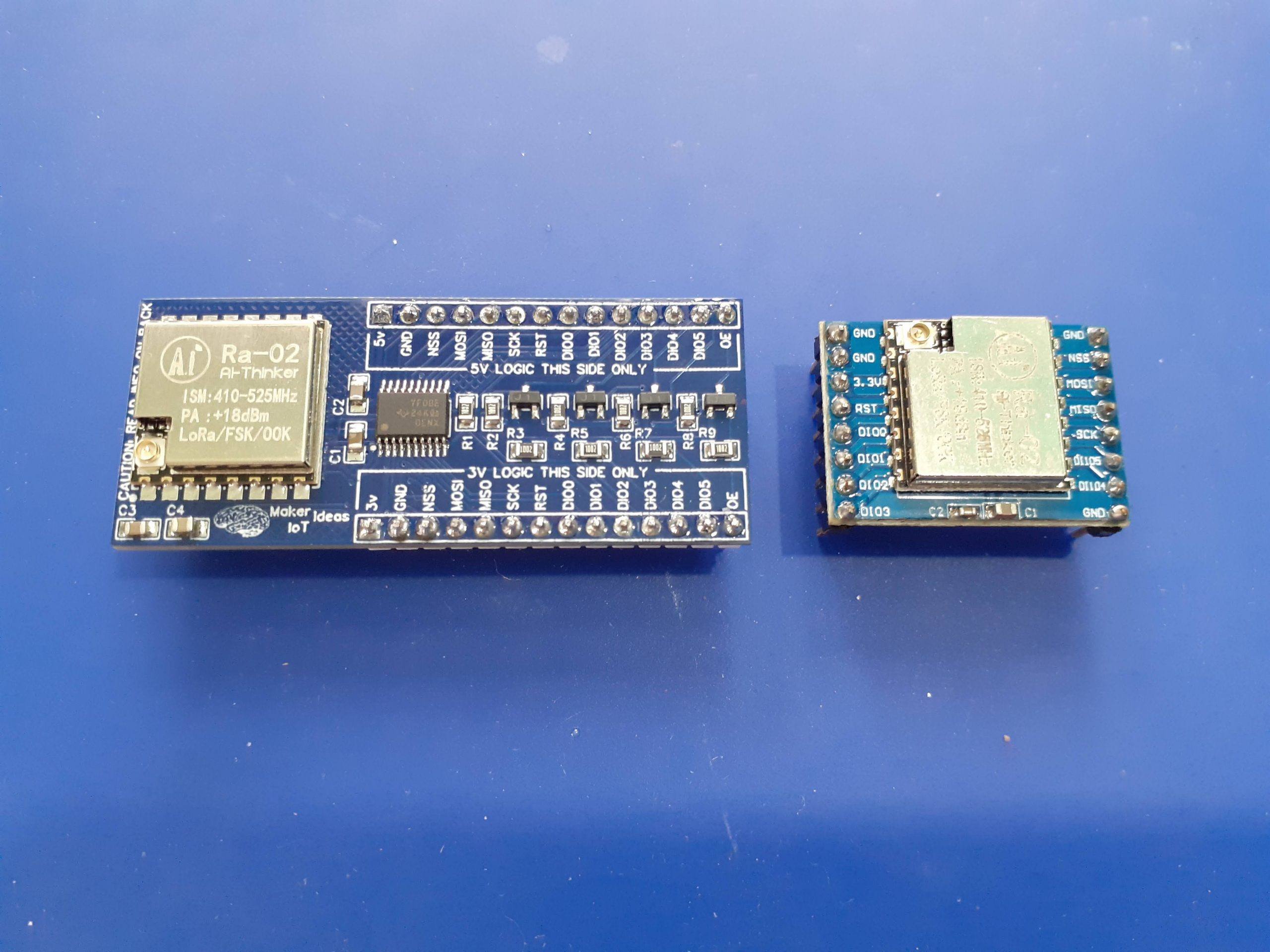
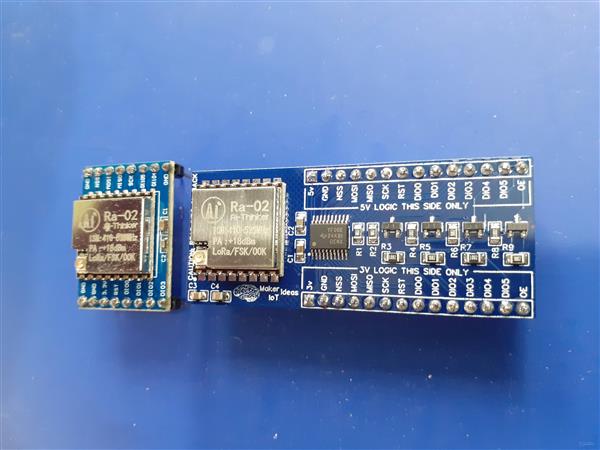
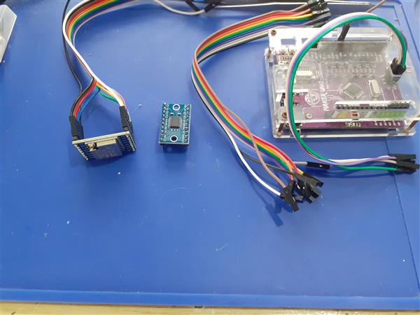
Most Makers and electronics enthusiasts may already know of the RA-02 LoRa Module. Many of them might own an RA-02 Breakout module or two… For those who do, they will surely know about the problems encountered with using this particular breakout module…
The RA-02 module, in itself, is a great piece of kit, and when used on a custom PCB, which was designed with all the little secrets of this module taken into consideration, is a pleasure. Using the RA-02 breakout module, in its existing form factor, does however present quite a few unique challenges, which, if you are unaware of them, can cause quite a few frustrating moments, or even result in permanent damage to the module…
1) The module is based on the SX1278 chip from Semtech and is a 3v device. The IO pins are NOT 5v compatible but seem to work for a few hours or so when used with 5v… This causes many people, especially on Youtube, to assume that it is ok to send 5v logic signals to this module…
I have still not seen any Youtube video telling viewers to at least use a resister divider or logic converter… People just don’t know, and those that know seem to be keeping quiet!
Adding logic converters is in fact specified by the datasheet.
2) Adding logic converters means adding additional wiring, and for a breadboard based project, that adds to the complexity.
3) You have a total of 4 ground pins that need to be connected. not connecting all of them, causes funny things to happen, from overheating down to failure… ( My personal experience while researching this project)
4) The existing breakout module is not breadboarding compatible, resulting in a floating assembly with wires going everywhere, which results in unstable connections etc…
Basically something similar to the picture below:
In this picture, I have an existing RA-02 Breakout Module, with an 8 channel Logic converter and an Arduino Uno clone, along with all the needed wiring to make this setup possible… Quite a lot of wires indeed…
My solution:
I design and use quite a few LoRa PCBs and on all of them, I implement logic conversion using the BSS138 N-MOS Mosfet and 10k resistors. It is a cheap and reliable solution, but it can take up quite a lot of space on a PCB, as this means 11 Mosfets and 22 10k resistors if I were to provide level conversion to all of the RA-02’s GPIO and IO pins…
I also have the constant problem of many unnecessary wires, many of which sometimes fail straight out of the box, when prototyping something. I partly solved that by designing a few dedicated PCB solutions, but that is not always ideal,
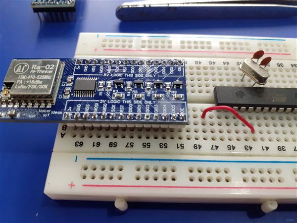
Using a dedicated Logic Converter IC, and Mosfet based converters to make up the difference, on a breadboard compatible module, seemed like a good idea, so I went ahead and designed the following solution:
The breakout board module is breadboard compatible, and also has clearly marked pins to indicate the 3v and 5v sides of the module.
For my first test, I decided to test with an Arduino Uno Clone, since that is what most Makers and students will have access to. I used Cytron’s Maker Uno platform, which is equipped with some added goodies, in the form of diagnostic LED etc to make prototyping a lot easier.
As we can clearly see, It is only necessary to connect to the 5v logic side of the module, as well as provide 3v and 5v + GND to the module
In this test, I used Sandeep Mistry’s LoRa Library, with the Arduino IDE to do a quick test sketch.
As we can see, you need quite a lot more wires to make this work. It is also worth noting that we have only 8 level converters on this ATMEGA328P PCB, in order to use all of the RA-02’s GPIO, we will need to add an additional external logic converter as well.
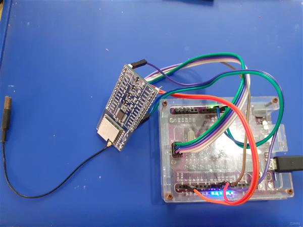
For my second test, I decided to be a bit brave, and try to use the new Raspberry Pi Pico ( RP2040 Microprocessor ). I have quite a few of them lying around and have never really done a lot with them, due to the fact that I do not really like using MicroPython or CircuitPython, and also because the recently released Arduino Core for the RP2040 still being quite new… I decided to use a development board that I recently bought from Cytron, the Maker Nano RP2040, as it has all the added diagnostic features to make my life a bit easier, I will also include a test with an original Pi Pico board, to make it more accessible to everyone out there.
Once again, I used Sandeep Mistry’s LoRa Library, with the exact same Arduino sketch, used for the Maker Uno test. (I obviously needed to change the pin numbers though, as the RP2040 uses different pins for its SPI interface).
Maker Nano RP2040 RA-02 Breakout Module
NSS 17
MOSI 19
MISO 16
SCK 18
RST 9
DIO0 8
In this case, we DO NOT need the OE pin, as the RP2040 is a native 3v device. The level converter can thus stay disabled, with its pins in tri-state ( high impedance ) mode.
If we look at the code, it is similar to the Maker Uno’s code, with only the Pin declarations needing a change
#include <SPI.h> // include libraries
#include <LoRa.h>
const int csPin = 17; // LoRa radio chip select
const int resetPin = 9; // LoRa radio reset
const int irqPin = 8; // change for your board; must be a hardware interrupt pin
byte msgCount = 0; // count of outgoing messages
int interval = 2000; // interval between sends
long lastSendTime = 0; // time of last packet send
// Note that SPI has different names on the RP2040, and it has 2 SPI ports. We used port 0
// CIPO (Miso) is on pin 16
// COPI (Mosi) is on pin 19
// SCK is on pin 18
// CE/SS is on pin 17, as already declared above
I did not use a breadboard, in order to make things as easy as possible.
To make things a bit easier, without having to resort to using a breadboard, I decided to do the Original Pi Pico test using the Maker Pi Pico PCB. This PCB is basically a big breakout module, with detailed pin numbers and some diagnostic LEDs, but it also uses a native Pi Pico, soldered directly to the PCB, by means of the castellated holes… So, While technically not being a true standalone Pico, It makes my life easier and was thus used for the test, as I can be sure that the pins are labelled exactly the same as on the original Pico.
The code used for the Maker Nano RP2040 works perfectly, with no changes required.
This post is getting quite long by now, so I have decided not to include my tests of the ESP-12E ( NodeMCU ) or ESP32 development boards here as well… They also function as expected.
In Summary
When I started this project, I set out to solve a problem ( personal to me ), that could potentially help a lot of other people use the RA-02 Module for more projects and tasks. The Breakout module in its current form can also be used with the RA-01h module (915Mhz Module) without any changes. All GPIO pins are broken out, and accessible through full logic converted pins on both sides of the breakout module.
I hope that this will be useful to someone. I am also not releasing the full schematics at this stage, as I may decide to make some minor cosmetic changes in the near future.
The PCB can however be ordered from PCBWay in its current form and works 100% as expected. The BOM file is available with the ordered PCB as usual.
This PCB was manufactured at PCBWAY. The Gerber files and BOM, as well as all the schematics, will soon be available as a shared project on their website. If you would like to have PCBWAY manufacture one of your own, designs, or even this particular PCB, you need to do the following… 1) Click on this link 2) Create an account if you have not already got one of your own. If you use the link above, you will also instantly receive a $5USD coupon, which you can use on your first or any other order later. (Disclaimer: I will earn a small referral fee from PCBWay. This referral fee will not affect the cost of your order, nor will you pay any part thereof.) 3) Once you have gone to their website, and created an account, or login with your existing account,
4) Click on PCB Instant Quote
5) If you do not have any very special requirements for your PCB, click on Quick-order PCB
6) Click on Add Gerber File, and select your Gerber file(s) from your computer. Most of your PCB details will now be automatically selected, leaving you to only select the solder mask and silk-screen colour, as well as to remove the order number or not. You can of course fine-tune everything exactly as you want as well.
7) You can also select whether you want an SMD stencil, or have the board assembled after manufacturing. Please note that the assembly service, as well as the cost of your components, ARE NOT included in the initial quoted price. ( The quote will update depending on what options you select ).
8) When you are happy with the options that you have selected, you can click on the Save to Cart Button. From here on, you can go to the top of the screen, click on Cart, make any payment(s) or use any coupons that you have in your account.
Then just sit back and wait for your new PCB to be delivered to your door via the shipping company that you have selected during checkout.
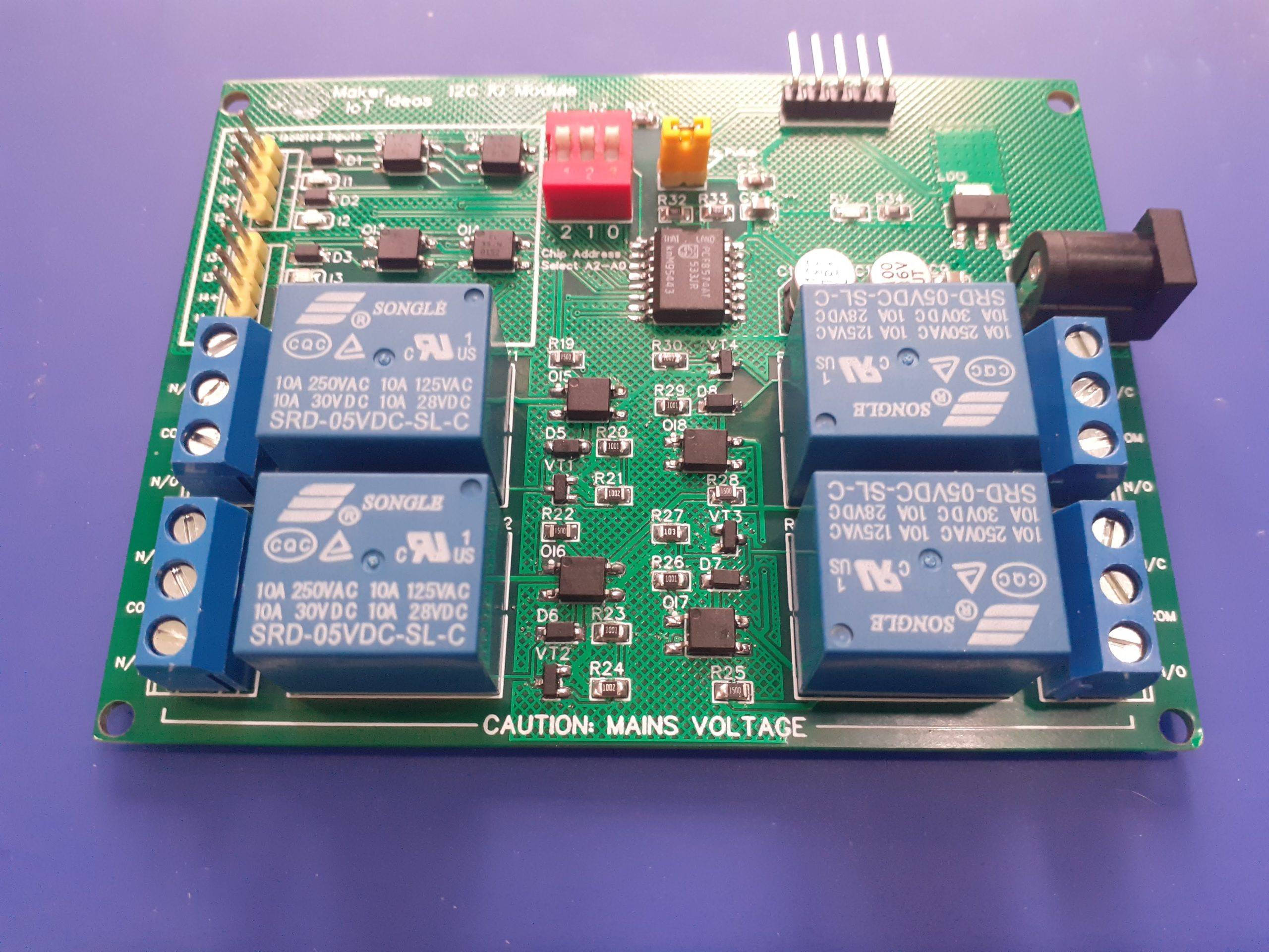
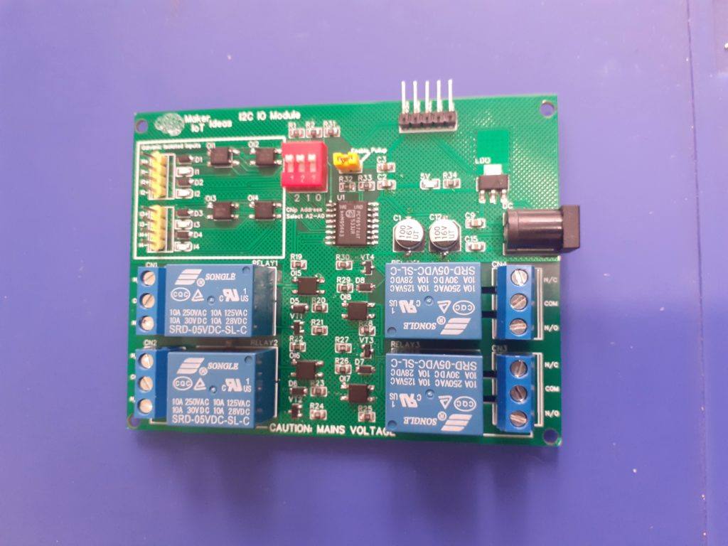
Sometimes we need extra Inputs or Outputs on a device, or for use with a project. To implement it properly we also need a lot of additional electronic components to properly isolate these inputs and outputs, with the signals they switch, from our own project, because, let us be real, electronics and electrical devices in the real world do not all work with Arduino or ESP32/ESP8266 save voltages ( 5v and 3.3v ).
I will also tell you about a very special deal to get PCBs of your own made for only one (1) USD ( Including shipping with DHL )! No, I am not joking, and I am not crazy either… More on that later in the post…
It is thus extremely important to have a module that can effectively interface with inputs of 5.5v up to 32v DC ( optically Isolated up to 3000v ), and relay outputs, also optically isolated at 3000v. ( Note that the optical isolation voltage does not mean you can input that voltage level into the chip! It means that it can isolate the electronics on the safe side of the isolator from a voltage spike of up to that voltage!).
I also love using I2C, as it allows me to add modules onto an existing data bus while using only 2 GPIO lines on the MCU!
The module I am presenting to you today was designed to be operated from 5v DC. That includes the I2C data lines (SDA and SCL). If you need to interface to a 3.3v microprocessor, like an ESP32 or ESP8266, or even the new RP2040 or an STM32, you need to use a logic level converter.
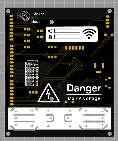
The PCB uses the popular PCF8574 8 channel IO expander, which is extremely easy to use, and where you can connect up to 8 devices in a chain ( 16 if you use the PCF8574AT variant as well.. Meaning eight of each variant) This surely adds up to quite a lot of IO lines at a cost of only 2 GPIO on your MCU!
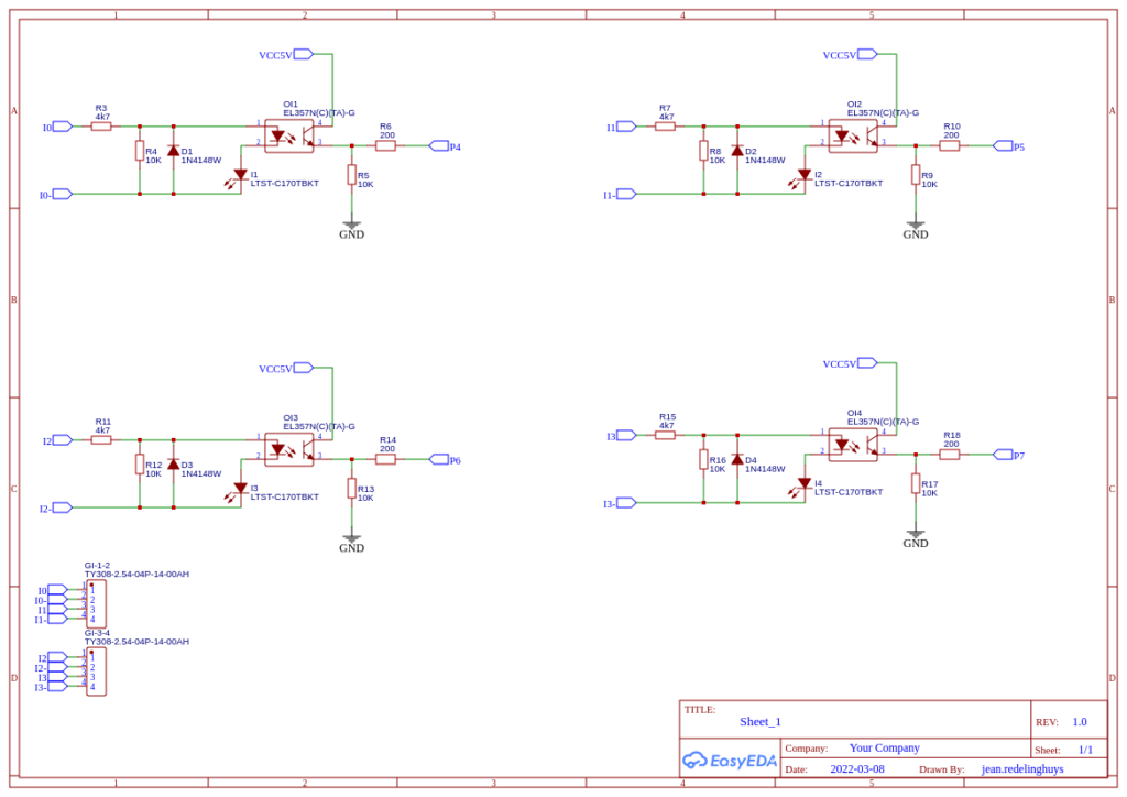
The Circuit diagram is below, and I will discuss each part briefly.
Schematic – Page 1
This is the Galvanic Isolated Input schematic. Each input operates at a voltage of 5.5v to 32v DC. Complete Galvanic Isolation between the Module and the remote input is in effect. Please note that you have to supply a remote ground from the device that provides the input. DO NOT connect the PCB Module ground to an isolated ground pin. This may still work but renders the galvanic Isolation for that input completely useless.
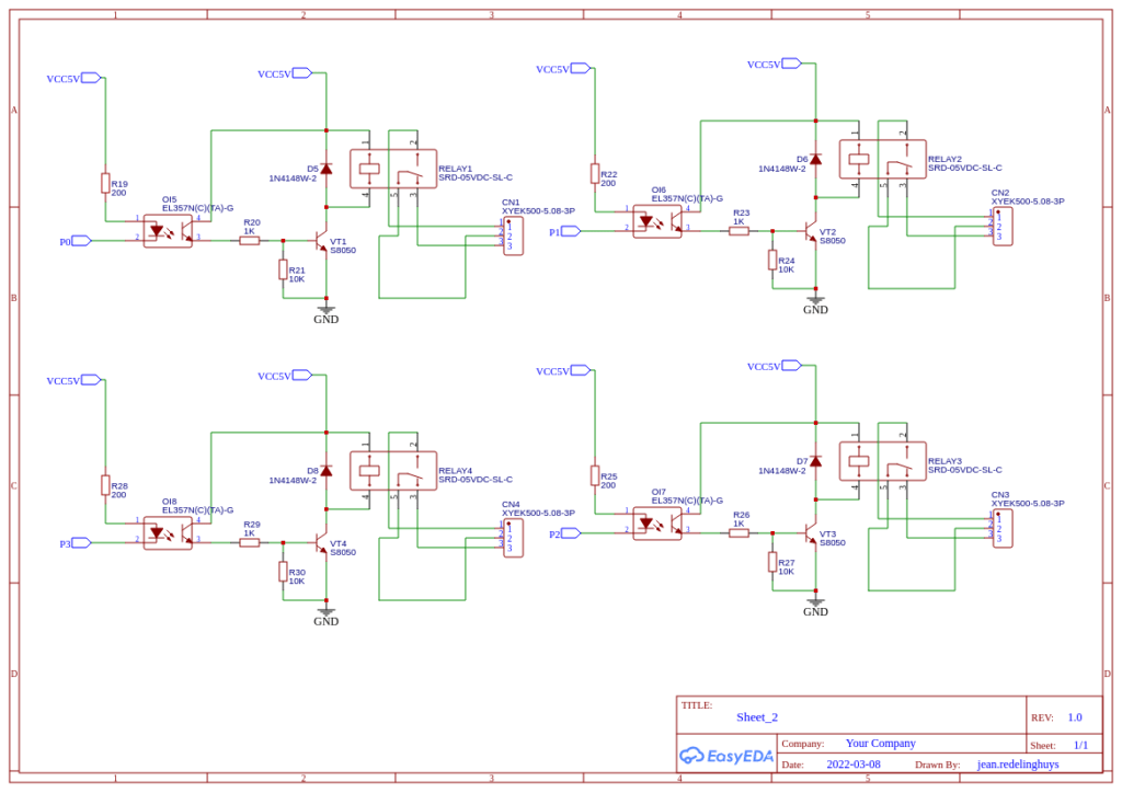
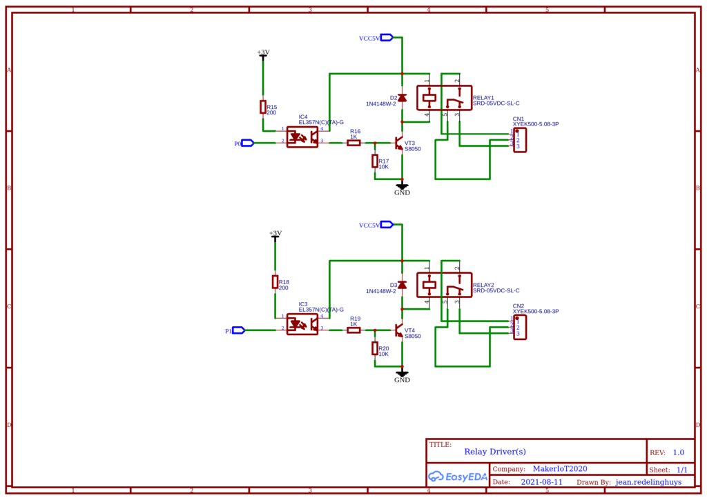
Relay Driver Schematic
This is the Relay driver schematic. Each relay output is driven through an optocoupler, as well as a transistor. Although this arrangement does not provide complete galvanic Isolation of the relay coil, it does protect your MCU from any voltage spikes caused by back-emf when the relay is de-energised. The Relay contacts themselves, being magnetically actuated by the coil, are in themselves Galvanically Isolated from the rest of the PCB.
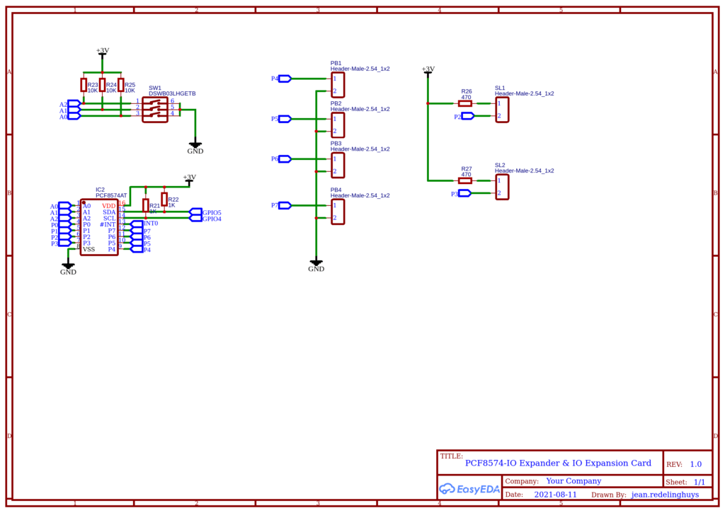
I2C Control Schematic
Finally, we have the I2C IO Expander schematic, with a 5v LDO regulator, capable of providing up to 600mA of current to the PCB. The PCF8574 Chip’s address is selectable with DipSwitch SW1 so that you can use multiple PCBs at the same time if you should choose to do so. The only note on that is that you should not connect the 5v lines of each individual PCB together. You should also only connect the GND and SDA, SCL lines back to the MCU.
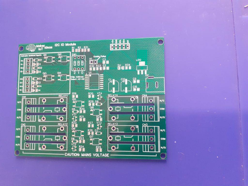
Raw PCB Layout
Earlier on in the post, I promised to tell you about a very special deal…
Well, here it is, as well as some details about the sponsor of this very exciting deal…
PCBPartner.com is owned and operated by Kinji Group, which was established in 1997. We have over 20 years of experience in PCB manufacturing, PCB design, component manufacturing and distribution, PCB assembly and PCB cam software development.
While Kinji Group has 3 PCB factories in China, we have also developed strategic partnerships with more than 15 other factories around Asia. We, therefore, have a large group of specialists in PCB manufacturing, quality control, technical support and part sourcing to support your innovative ideas and products.
Our over 500 employees are spread across 8 branches in Mainland China (Shenzhen, Dongguan, Shanghai, Wuxi, Chengdu, Xiamen), Hong Kong SAR, and Taiwan. And we’re still growing!
We’re confident once you try us out, we’ll become your PCB Partner. And if not? Well, you’ll have scored some free PCB! So why not take us for a spin, you’ve got nothing to lose.
We, MakerIoT2020.com, have decided to give it a go and send this particular PCB to PCBPartner.com for manufacturing. So far, while we are still waiting to receive the PCB, ( Weekends happen 🙂 ), We are very happy with the ease of use of the online ordering system provided.
We would also like to point out that this special order will only be available until the end of March 2022, as well as that there are a few conditions:
Promotion ends March 31st 2022 Each new customer can enjoy free PCB on their first order This promotion applies to 1-2 layers of FR4 PCB, up to 100x100mm, 10pcs, with Green Solder Mask 4 layer of FR4 PCB, up to 50x50mm, 10pcs, with Green Solder Mask 1 layer Aluminum PCB, up to 100x100mm, 10pcs This PCB promotion cannot be used with other discounts or other promotional activities
For a full list of conditions, and countries that may participate in this offer, please click on the link here
Let us have a look at the entire ordering process..
Once you click on the PCBPartner.com link, you will be taken to their website, where you should sign up, which is free and easy… We used our Google.com account details and were ready to order in seconds…
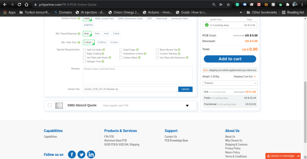
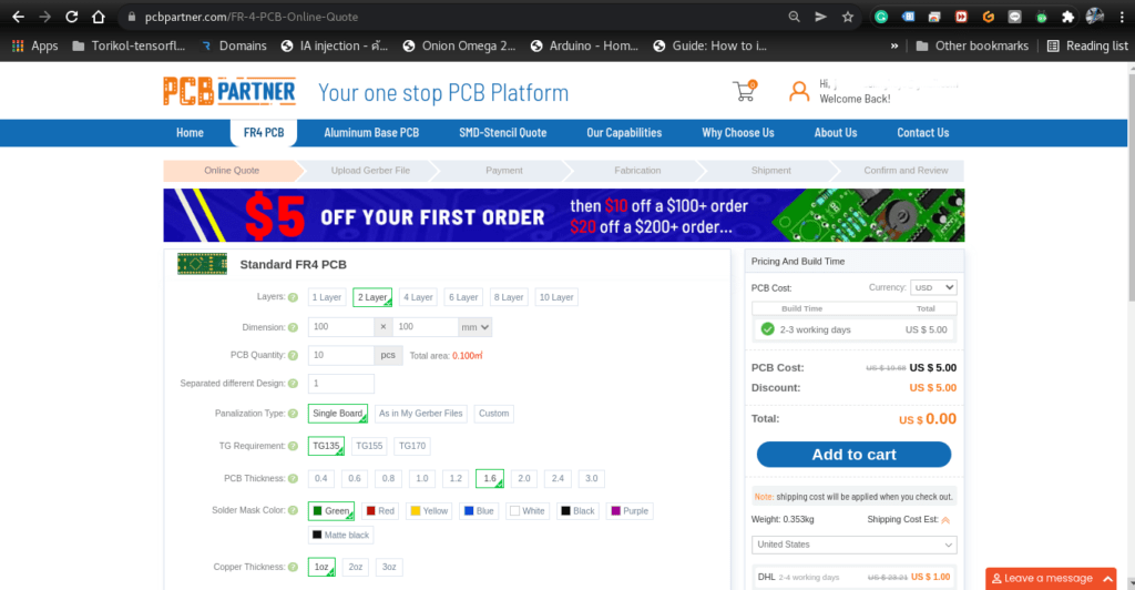
FR4 PBC Quote Form – Before uploading your Gerber Files
Enter the specific details for the manufacturing of your PCB, and upload your Gerber files.
After uploading your Gerber Files.
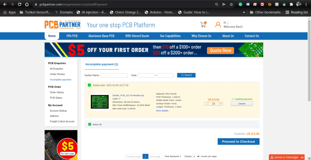
Continue selecting options for your PCB order… Make sure to select DHL shipping, to take advantage of the special 1USD option, and click on the ADD to Cart Button…
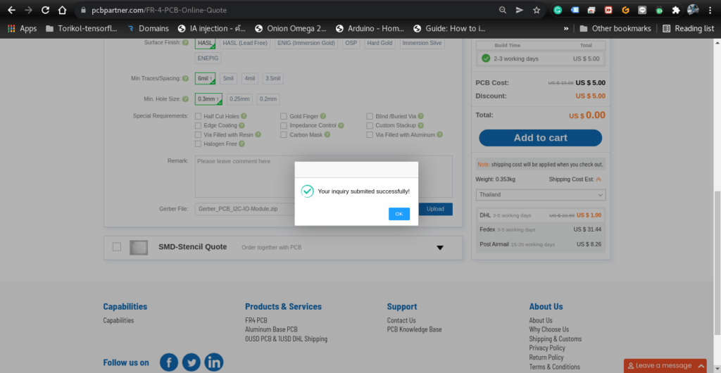
Quote added to your shopping cart.
You will now get a message that your enquiry has been submitted successfully.
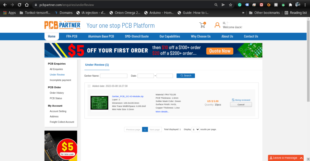
Click on the “Under review” button, to see your quote status… In my case, it took about 5 minutes for the review to pass, and be able to checkout and pay for the order…
PCB order under review
Once the review has passed, you will see a pending payment,
Payment Pending
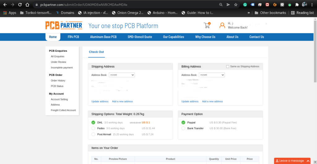
You may now click on the “Proceed to Payment” option
Add your shipping address, and choose your payment option.
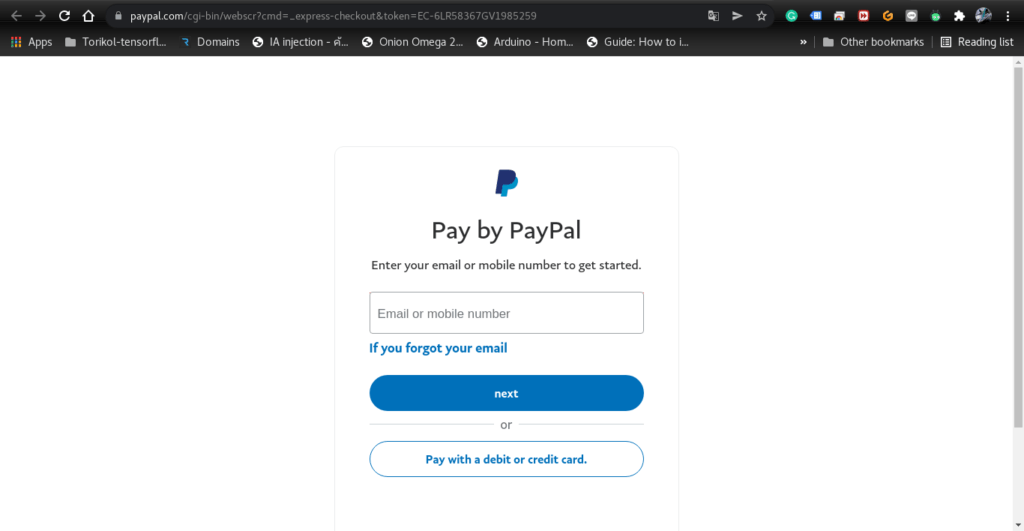
At this moment in time, only two payment options are supported, Paypal ( as well as Debit and Credit cards) and Direct Bank Transfer. I believe more options will be made available in future.. Checkout with Paypal
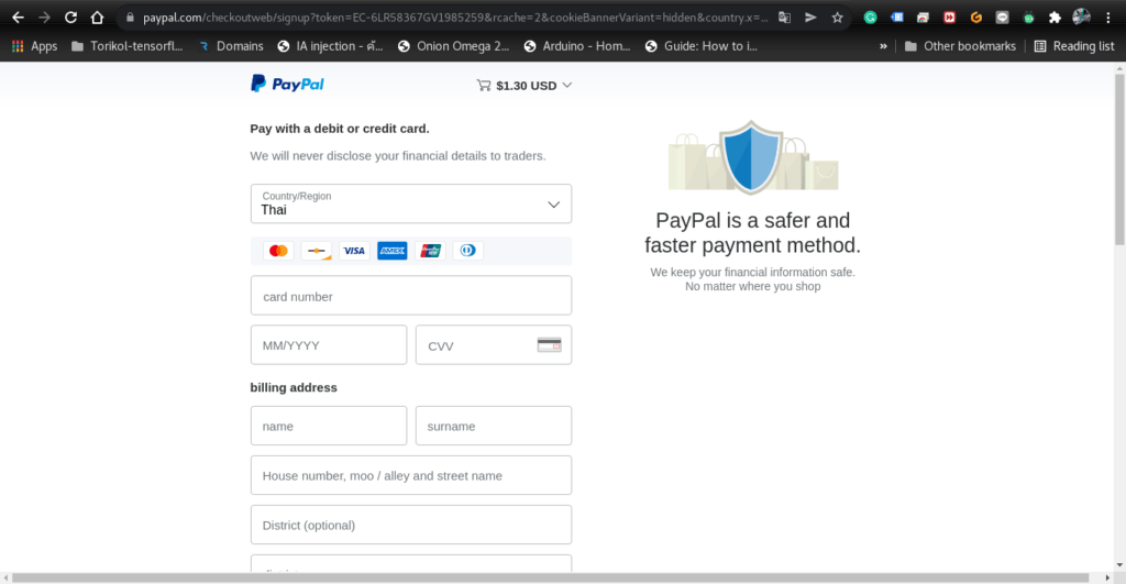
In my case, I chose Paypal and paid by Debit card.
Enter your card detailsAfter Payment.
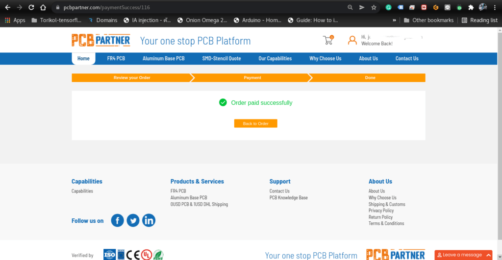
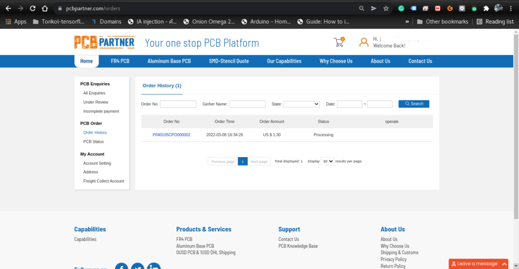
After payment was made successfully, you can also check on the status of your order…
Review your order status
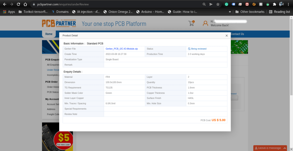
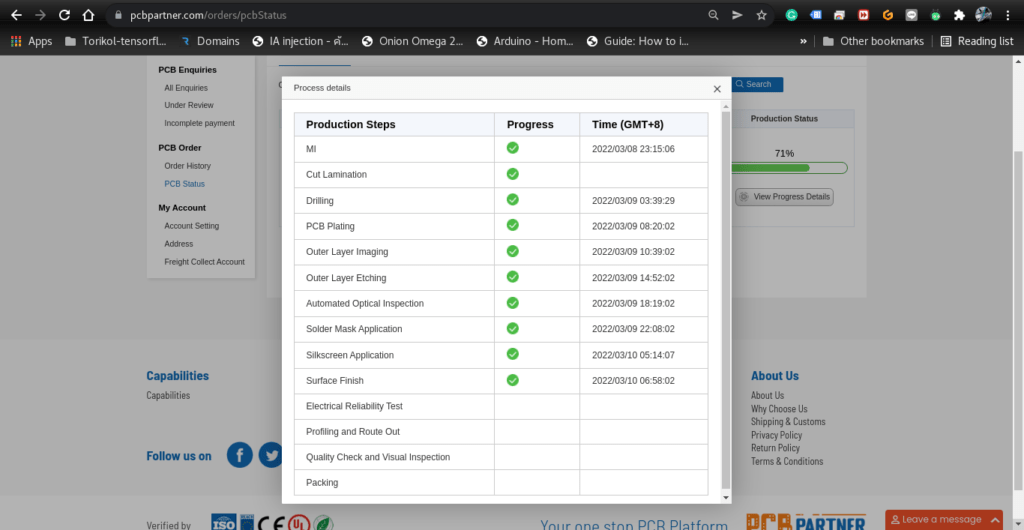
You can also review your order at any stage before or after payment, as well as get progress reports of the manufacturing process.
PCB Order Status.
In conclusion, I would like to say that it was quite easy to order and make payment. The Website is easy to use, and everything is clear and easy to understand. The PCB was well manufactured and seems to be quite good quality
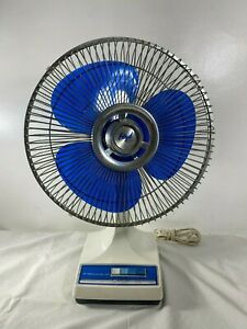
Desk or floor-standing fans are one of those appliances that will be present in almost every home or office. Some of the newer ones may already have remote control of some sort, while the older models won’t. It is however quite easy to do a retro-fitted controller to most of them, and at the same time, give them some (limited) intelligence.
Your typical oscillating fan does not have a lot of intelligence built-in. They normally consist of an electrical motor, with three separate windings, of varying inductance ( meaning the number of turns in the coil of wire will change the magnetic field generated, thereby changing the speed of the electric motor).
These windings have one common side, where all three of them are connected together, and the other three are separated. Normally the live wire from your mains supply (220v AC in my case) will go to this common connection. The neutral wire will go to the common of a four-position mechanical switch, with each winding going to one of positions 2,3 and 4 ( This results in a 3-speed configuration, with the first switch being off). It is also VERY important to note that this mechanical switch is hardware interlocked, meaning that ONLY one switch can be on at any given time… This is to ensure that electricity can only flow through one winding at a time. If you were to send electricity through multiple windings at the same time, the motor will still work, but not for very long…
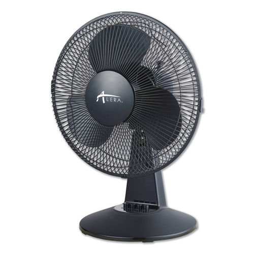
A more modern Oscillating Fan
In order to automate an oscillating fan, we would thus need a way to switch the separate windings on and off, while preventing other windings from getting power at the same time. I chose to do this with SPST relays, as a proof of concept, and plan to design it with DPDT relays at a later stage to implement a proper hardware interlock, in addition to the software interlock implemented in the control software ( more on that later)
My requirements for the device are the following: 1) Must operate from mains power, using the existing power cord of the fan. 2) Must allow for local operation of the fan using the existing control buttons. 3) Must be able to update firmware OTA, and have WiFi connectivity for control via Home Assistant or MQTT 4) Must be capable of adding support for ESP Now protocol at a later stage 5) The fan must not have any visible modifications on the outside
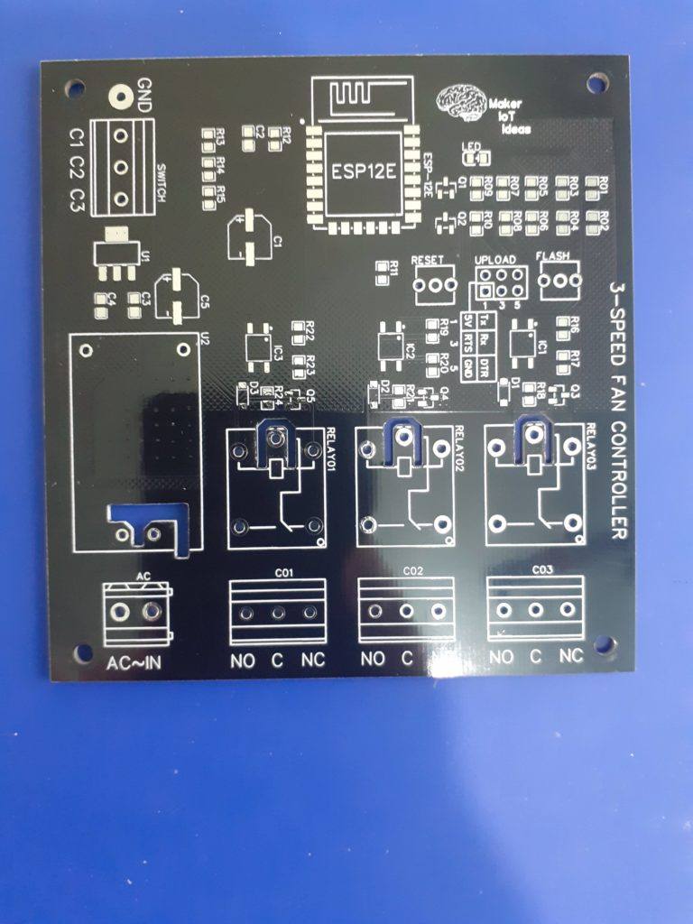
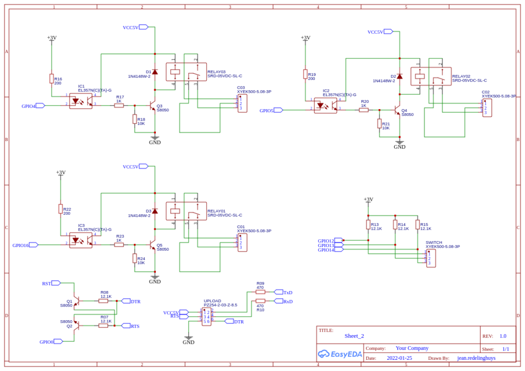
The 3 speed Fan controller PCB
Taking all of my requirements into consideration, I have designed the following PCB to take care of my needs. As I do not require a lot of GPIO for this ( only 3 outputs, and 3 inputs ), I have decided to use an ESP8266-12E module from Espressif ( manufactured by AITinker, not sponsored by either company). This module is relatively cheap and has more than enough flash memory, RAM, as well as GPIO available.
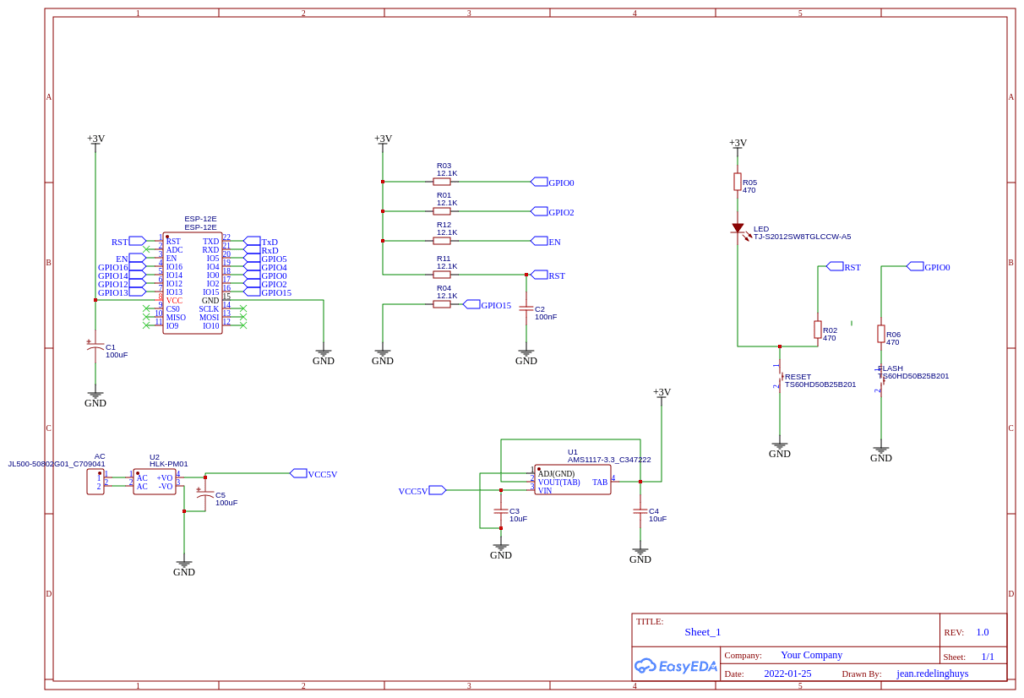
Circuit Diagram – Page 1Circuit Diagram – Page 2
As we can see, the circuit is minimal, with optical isolation on the relay drivers, a programming header, and a 3-way input for the mechanical switch.
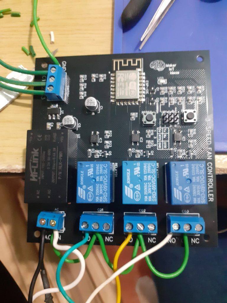
The completed PCB, wired to the oscillating fan
As seen in the picture above, the wiring is quite simple, with the neutral wire looped to the common terminal of each relay (I had only green mains rated cable available, will replace it later with a proper white cable to keep to wiring standards). Black is live, with one wire going to the mains socket, and the other to the common of the motor coil windings. Light blue, yellow and white ( connected to the N/O terminal of the relays) corresponds to speeds 1, 2 and 3 of the fan.
At the top of the board, 3 wires go to the mechanical switch and a fourth to DC ground. (Note that there is no AC voltage on any of the switches. )
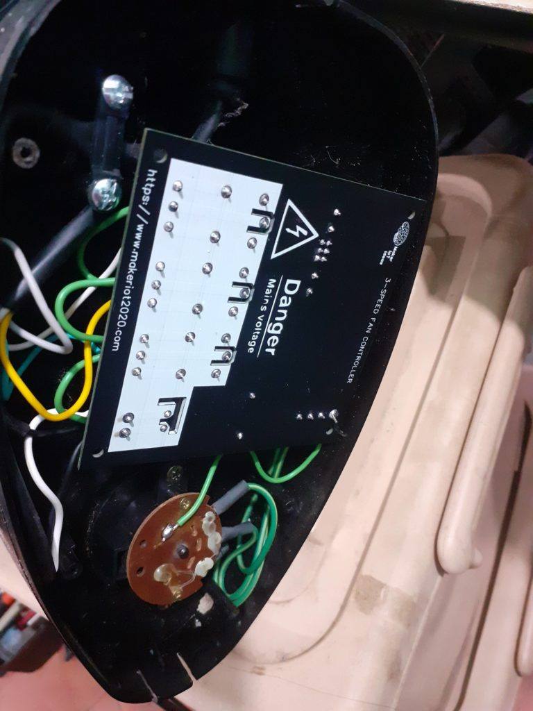
Mounting the PCB in the base of the oscillating fan
The PCB is mounted in the base of the fan while taking care to ensure that no AC cables are near the DC components. The ESP8266 chip is oriented to the side ( logo side of PCB ) to prevent interference to the WiFi signal. The mechanical switch is mounted into its original position, and its wires are routed away from any AC carrying wires to prevent interference.
It is important to note here that the firmware for the PCB was uploaded before assembly. You should NOT attempt serial uploading while the device is connected to mains power under any circumstances. ( While I have taken every precaution to ensure that AC and DC components of the circuit are separated from each other, it is just common sense to not try to upload firmware with mains connected)
The completed PCB shows the Upload port near the right top corner.
Uploading firmware:
Initial uploading of firmware can be performed by connecting a USB-to-serial adapter to the UPLOAD port and providing 5v and ground from the USB-to-serial adapter. The flash button is held down, and the board is reset, after which you can proceed with uploading, alternatively, you can also connect the DTR and RTS lines from the serial adapter to automatically reset the board and enter flash mode as needed. ( If your adapter supports this of course).
ESPHome configuration
The YAML configuration for ESPHome is listed below:
This PCB was manufactured at PCBWAY. The Gerber files and BOM, as well as all the schematics, will soon be available as a shared project on their website. If you would like to have PCBWAY manufacture one of your own, designs, or even this particular PCB, you need to do the following… 1) Click on this link 2) Create an account if you have not already got one of your own. If you use the link above, you will also instantly receive a $5USD coupon, which you can use on your first or any other order later. (Disclaimer: I will earn a small referral fee from PCBWay. This referral fee will not affect the cost of your order, nor will you pay any part thereof.) 3) Once you have gone to their website, and created an account, or login with your existing account,
4) Click on PCB Instant Quote
5) If you do not have any very special requirements for your PCB, click on Quick-order PCB
6) Click on Add Gerber File, and select your Gerber file(s) from your computer. Most of your PCB details will now be automatically selected, leaving you to only select the solder mask and silk-screen colour, as well as to remove the order number or not. You can of course fine-tune everything exactly as you want as well.
7) You can also select whether you want an SMD stencil, or have the board assembled after manufacturing. Please note that the assembly service, as well as the cost of your components, ARE NOT included in the initial quoted price. ( The quote will update depending on what options you select ).
8) When you are happy with the options that you have selected, you can click on the Save to Cart Button. From here on, you can go to the top of the screen, click on Cart, make any payment(s) or use any coupons that you have in your account.
Then just sit back and wait for your new PCB to be delivered to your door via the shipping company that you have selected during checkout.
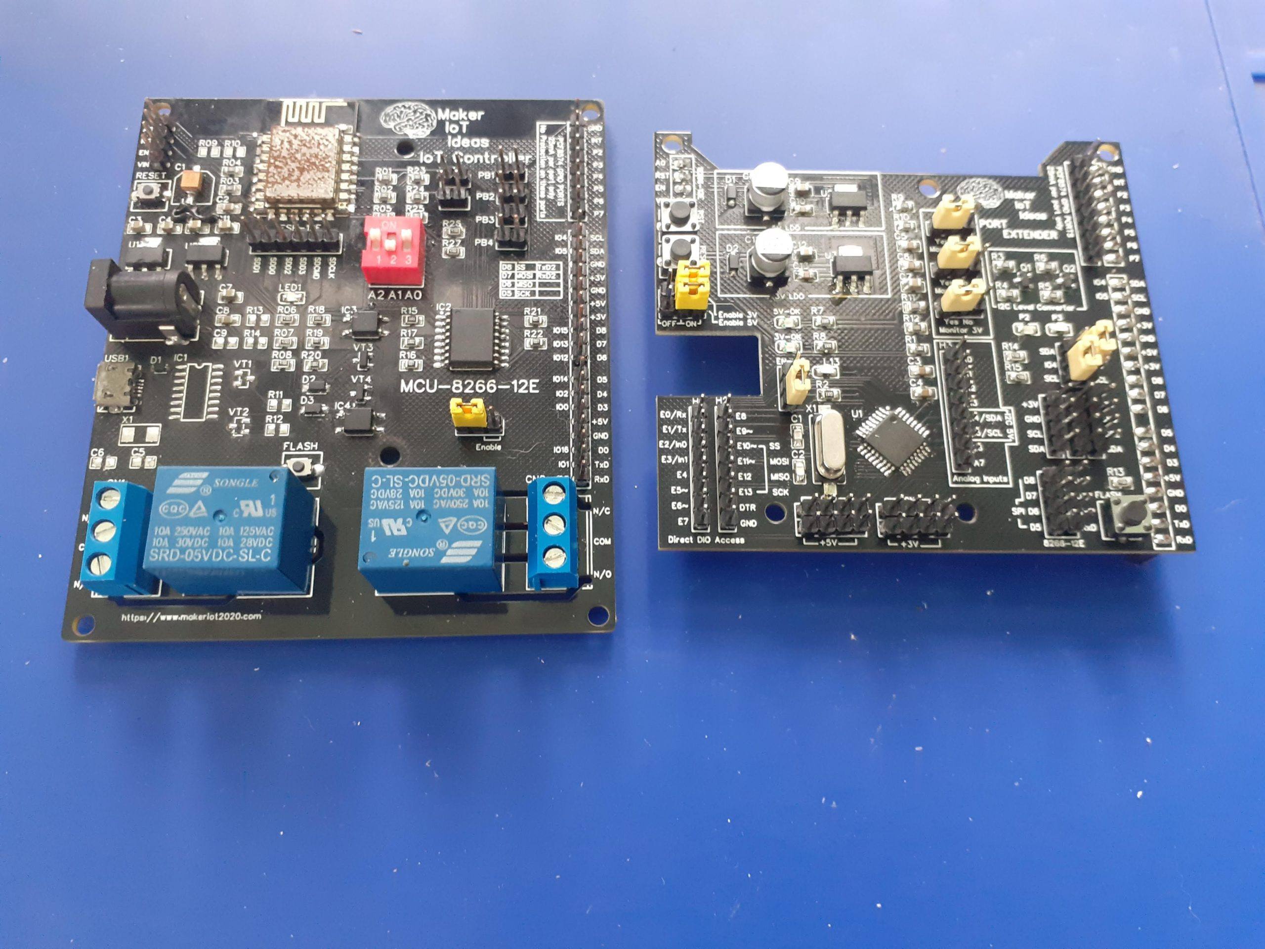
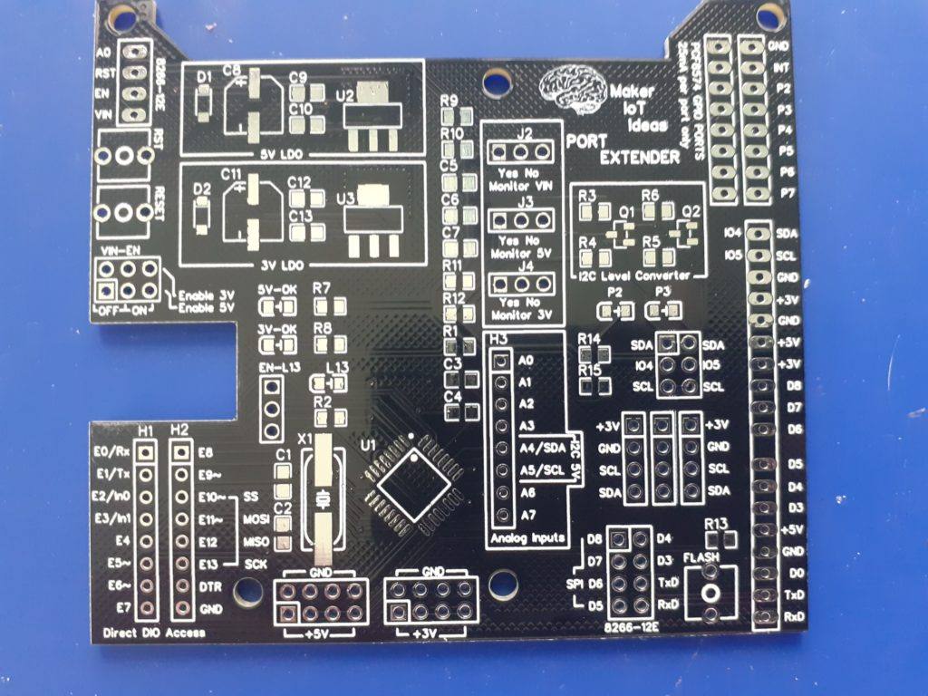
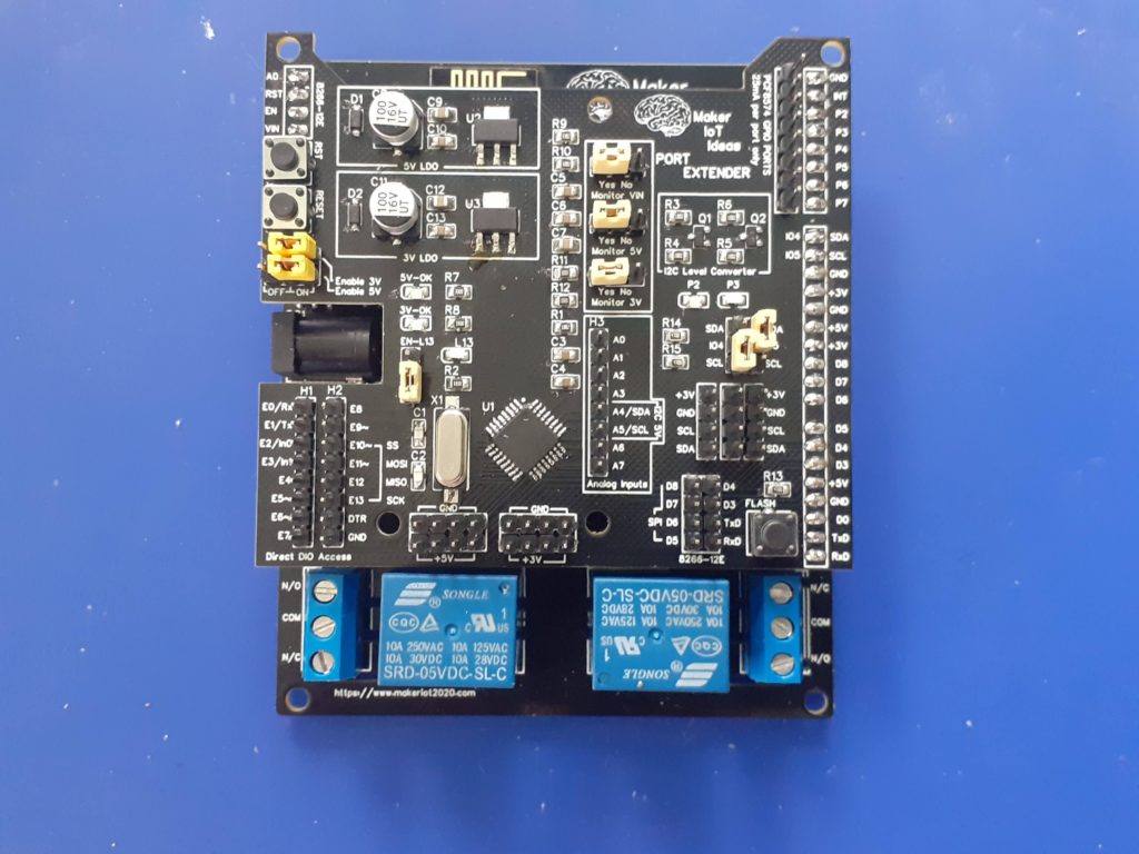
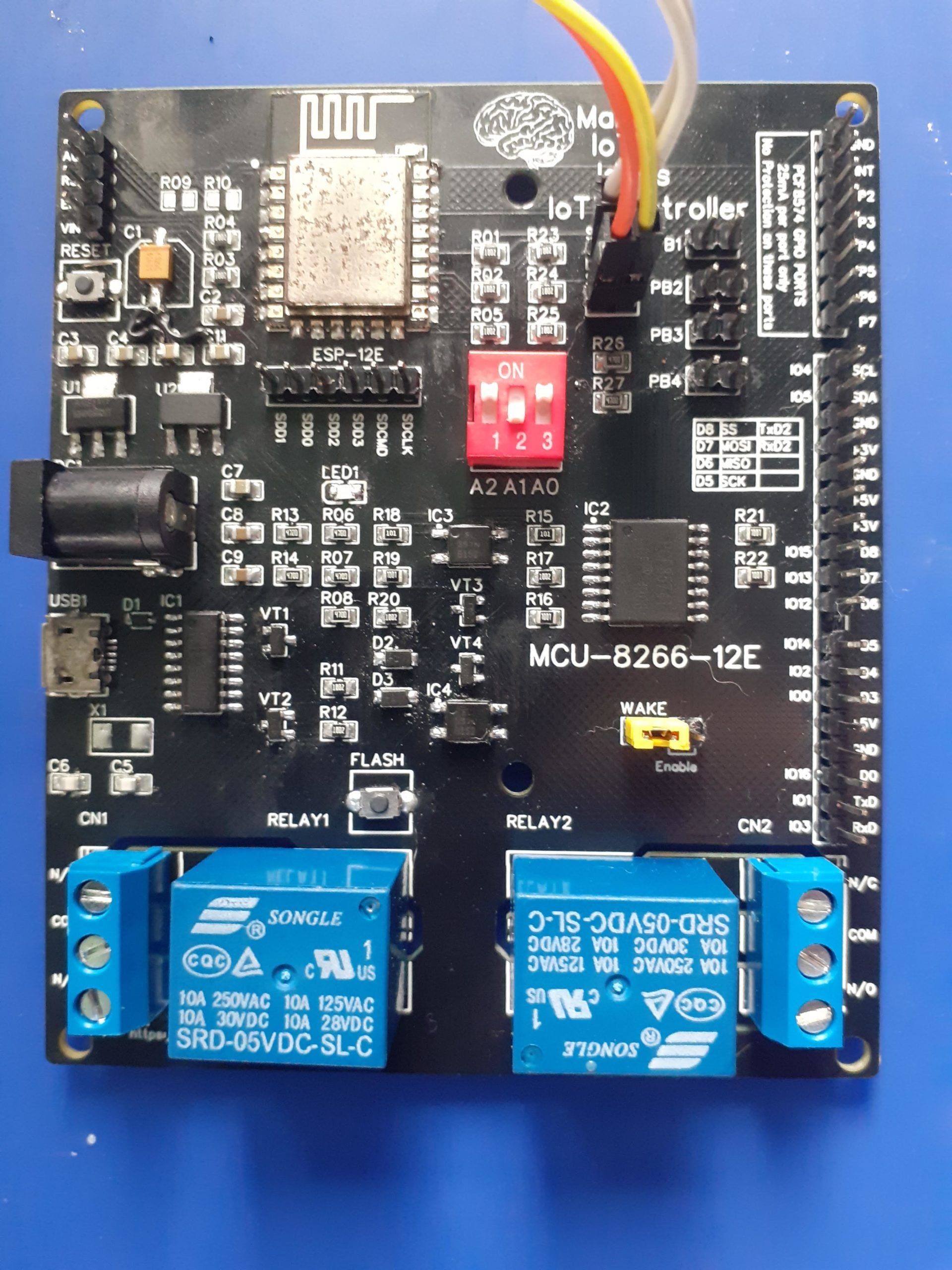
After quite a few experiments, and playing with a lot of ideas, we have finally produced and tested an almost final prototype for the MCU-8266-12E IoT Controller Port Extender Card. While the baseboard already has quite a lot of free GPIO pins for additional sensors and devices, It did however have quite a few issues, namely a lack of sufficient Power outputs, difficulty access to the I2C bus, as well as only 2 relay outputs. Granted that you do have access to unused pins on the PCF8574 Port Extender, We nonetheless decided that an add-on card would definitely make sense to allow this device to really be more useable.
While looking at various ideas for this card, the most flexible seemed to be the APE Protocol device as documented in ESPHome. They used a standard Arduino board for that, but we decided that, after testing it with an Arduino Nano, since it seems to work well, let us just design a dedicated PCB. It also looks much better as well 🙂
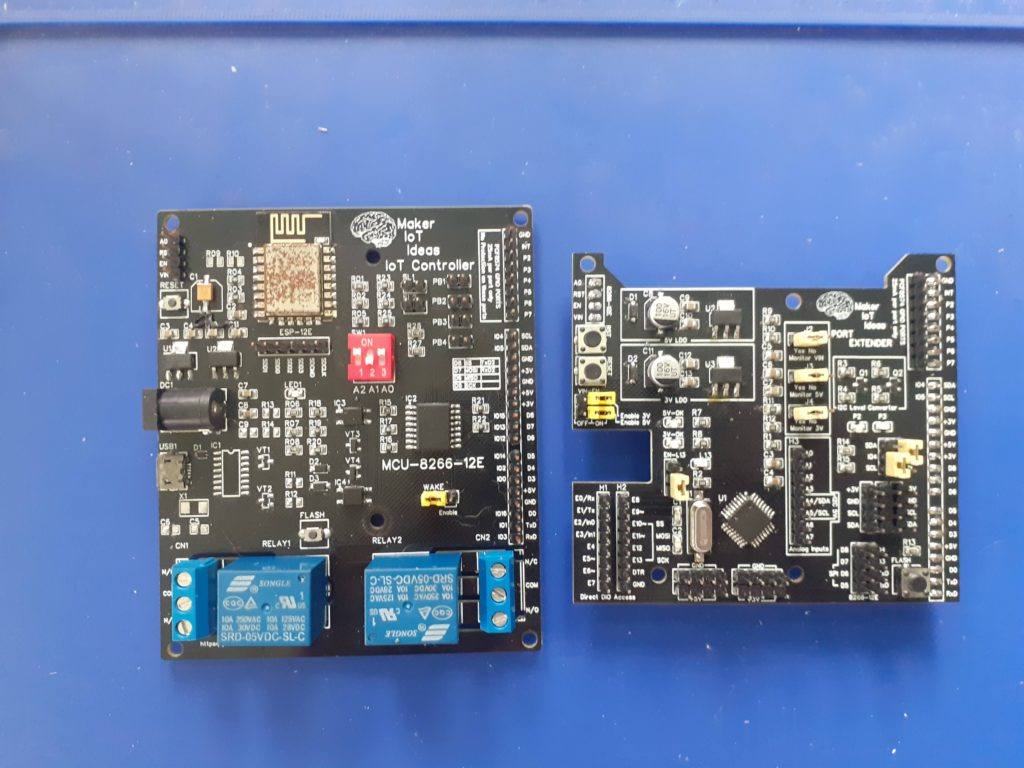
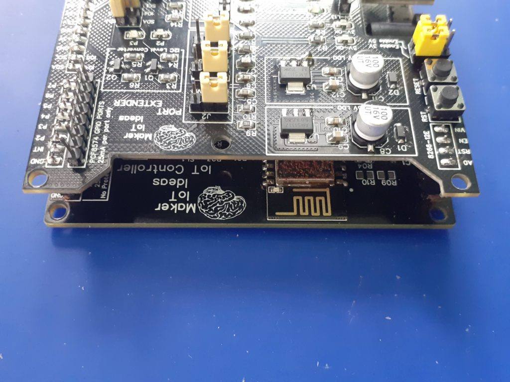
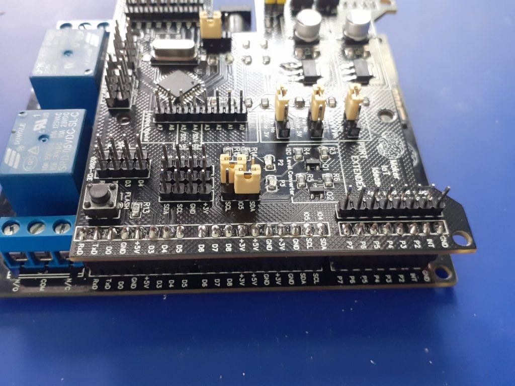
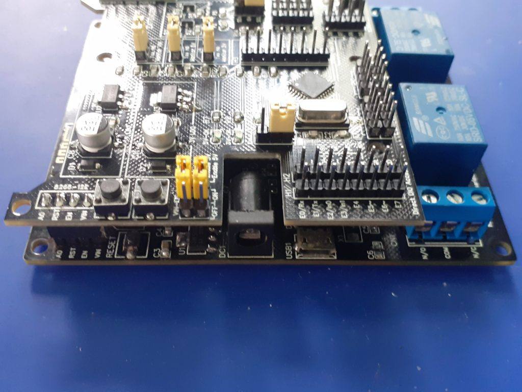
The beginning of the APE (Arduino Port Extender) Device. MCU-8266-12E with Arduino Nano (left) and MCU-8266-12E with the newly designed APE Card (right)
Some Features (Aside from being a fully functional Arduino clone as well)
1). Dedicated LDO Regulators for 5v and 3.3v (800mA each), with jumpers to switch them on or off (receive power only from the IoT Motherboard). 2.) Dedicated Logic Level Converter on the I2C Bus ( This is sort of very much needed 🙂 The Atmega 328P-AU is running at 5v on this device, to enable it to run at 16Mhz.. and the ESP8266 on the Motherboard is a 3.3v device..
There are also 3x 3.3V I2C Headers, complete with 3.3v and Ground, as well as a single 5v I2C header 3). 8 Analog Inputs ( While practically you can only use 6 of these if you use I2C ) 4). Voltage Divider provided on A0 to measure VIN ( to be safe, we calculated the resistors for 22v) 5). 100R current limiting resistor on A1 and A2, to measure 5v and 3.3v as well… Analog inputs A0, A1 and A2 can be switched back to normal operation by changing the jumper at J2,J3 or J4 from On to Off. 6). 12 Digital Inputs/Outputs (14 if you use D0 and D1 as well), as well as a Jumper to remove the LED on D13. 7). Full access to the PCF8574 and ESP8266 Pins from the motherboard below.
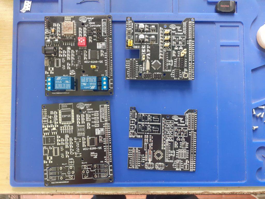
Pictures of the PCB
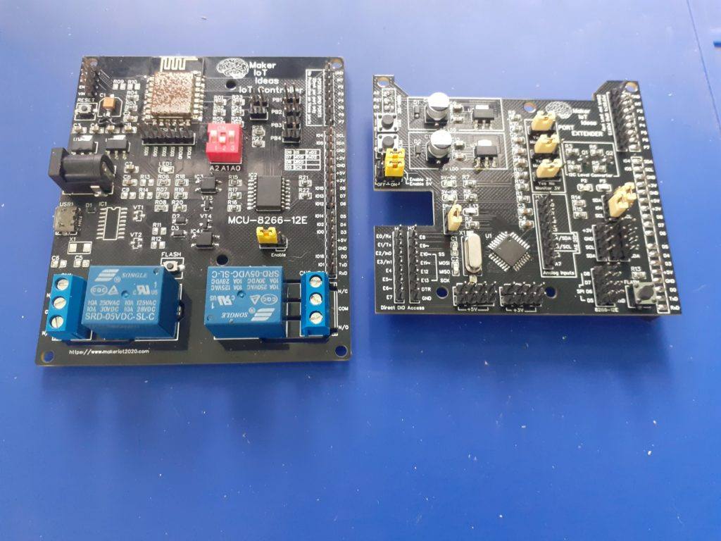
Side by side MCU-8266-12E (left) 8266-12E-Port Extender (right)
Side by side MCU-8266-12E (left) 8266-12E-Port Extender (right)
Side by side MCU-8266-12E (left) 8266-12E-Port Extender (right) [ with unpopulated PCB at bottom]
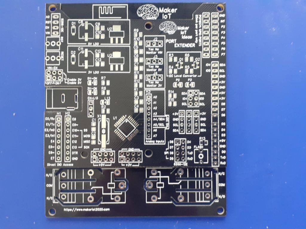
Blank PCB 8266-12E-Port Extender
Blank PCB MCU-8266-12E IoT Controller
Top view 8266-12E PE
8266-12E-PE side view { from bottom)
Right side view – 8266-12E-PE
Left side view – 8266-12E-PE
Stacked on-top-of MCU-8266-12E
Stacked – Top Side view
Stacked – Right side view
Stacked – Left side view
Pictures of the PCB, alone and with the MCU-8266-12E IoT controller
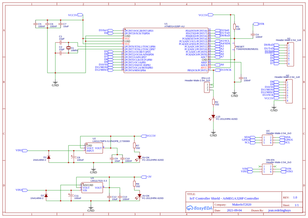
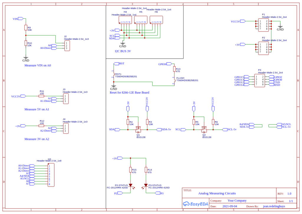
Circuit Diagram
ATMega328P-AU Circuit diagram with LDO Regulators, headers and supporting circuitry.Analog measuring circuitry, level converters and supporting circuitry and headers
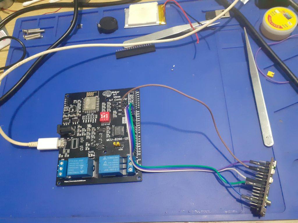
Uploading Code to the ATMega328P
Uploading code to the device requires the use of either an ISCP programmer ( Arduino as ISP works well ) or in the case of a pre-boot loaded chip, a USB-to-Serial converter. We did not find it necessary to add a dedicated USB-to-Serial converter onto the PCB. It is quite easy enough to do any flashing with the tools mentioned above.
Make sure that the PCB is not stacked when doing this. ( This will prevent excessive current use of other components when you supply 5v to the PE card.
Procedure to upload using ICSP
During assembly, you are required to solder a single 90-degree bend pin header on the bottom side of the PCB, in the same hole as the board side edge of the RESET push-button. This will serve as the RESET Pin for the ISCP. Other connections are as follows:
H2 Header <- > ICSP Programmer MOSI (E11~) – MOSI ( or Pin 11 on Arduino as ISP ) MISO (E12 ) – MISO ( or Pin 12 on Arduino as ISP ) SCK (E13) – D13 (or Pin 13 on Arduino as ISP ) RESET – D10 (or Pin 10 on Arduino as ISP )
5v and Ground from Arduino as ISP or ISCP Programmer to any 5v and ground pin on the PE Card
Please note the description above for assembly of the RESET pin header
Procedure to upload using USB-to-Serial converter
H1 Header
E0/Rx <- to Tx of USB-to-Serial converter E1/Tx -> to Rx of USB-to-Serial converter
H2 Header
DTR <-> to DTR of USB-to-Serial converter [ This connection is needed for successful uploading. Don’t leave it out ]
5v and Ground from the USB-to-Serial converter to any 5v and ground pin on the PE Card
Testing with ESPHome APE protocol and the MCU-8266-12E IoT controller
The following Arduino Sketch needs to be uploaded to the device. It will allow the device to function as a custom I2C device. Feel free to change the I2C address in the sketch as you choose, but remember to use the same address in your ESPHome YAML configuration file
The following C header file needs to be uploaded to your Home Assistant ESPHome folder.
// Must disable logging if using logging in main.cpp or in other custom components for the
//  __c causes a section type conflict with __c thingy
// you can enable logging and use it if you enable this in logger:
/*
logger:
  level: DEBUG
  esp8266_store_log_strings_in_flash: False
  */

//#define APE_LOGGING

// take advantage of LOG_ defines to decide which code to include
#ifdef LOG_BINARY_OUTPUT
#define APE_BINARY_OUTPUT
#endif
#ifdef LOG_BINARY_SENSOR
#define APE_BINARY_SENSOR
#endif
#ifdef LOG_SENSOR
#define APE_SENSOR
#endif

static const char *TAGape = "ape";

#define APE_CMD_DIGITAL_READ 0
#define APE_CMD_WRITE_ANALOG 2
#define APE_CMD_WRITE_DIGITAL_HIGH 3
#define APE_CMD_WRITE_DIGITAL_LOW 4
#define APE_CMD_SETUP_PIN_OUTPUT 5
#define APE_CMD_SETUP_PIN_INPUT_PULLUP 6
#define APE_CMD_SETUP_PIN_INPUT 7
// 8 analog registers.. A0 to A7
// A4 and A5 not supported due to I2C
#define CMD_ANALOG_READ_A0 0b1000 // 0x8
// ....
#define CMD_ANALOG_READ_A7 0b1111 // 0xF

#define CMD_SETUP_ANALOG_INTERNAL 0x10
#define CMD_SETUP_ANALOG_DEFAULT 0x11

#define get_ape(constructor) static_cast<ArduinoPortExpander *>(constructor.get_component(0))

#define ape_binary_output(ape, pin) get_ape(ape)->get_binary_output(pin)
#define ape_binary_sensor(ape, pin) get_ape(ape)->get_binary_sensor(pin)
#define ape_analog_input(ape, pin) get_ape(ape)->get_analog_input(pin)

class ArduinoPortExpander;

using namespace esphome;

#ifdef APE_BINARY_OUTPUT
class ApeBinaryOutput : public output::BinaryOutput
{
public:
  ApeBinaryOutput(ArduinoPortExpander *parent, uint8_t pin)
  {
    this->parent_ = parent;
    this->pin_ = pin;
  }
  void write_state(bool state) override;
  uint8_t get_pin() { return this->pin_; }

protected:
  ArduinoPortExpander *parent_;
  uint8_t pin_;
  // Pins are setup as output after the state is written, Arduino has no open drain outputs, after setting an output it will either sink or source thus activating outputs writen to false during a flick.
  bool setup_{true};
  bool state_{false};

  friend class ArduinoPortExpander;
};
#endif

#ifdef APE_BINARY_SENSOR
class ApeBinarySensor : public binary_sensor::BinarySensor
{
public:
  ApeBinarySensor(ArduinoPortExpander *parent, uint8_t pin)
  {
    this->pin_ = pin;
  }
  uint8_t get_pin() { return this->pin_; }

protected:
  uint8_t pin_;
};
#endif

#ifdef APE_SENSOR
class ApeAnalogInput : public sensor::Sensor
{
public:
  ApeAnalogInput(ArduinoPortExpander *parent, uint8_t pin)
  {
    this->pin_ = pin;
  }
  uint8_t get_pin() { return this->pin_; }

protected:
  uint8_t pin_;
};
#endif

class ArduinoPortExpander : public Component, public I2CDevice
{
public:
  ArduinoPortExpander(I2CBus *bus, uint8_t address, bool vref_default = false)
  {
    set_i2c_address(address);
    set_i2c_bus(bus);
    this->vref_default_ = vref_default;
  }
  void setup() override
  {
#ifdef APE_LOGGING
    ESP_LOGCONFIG(TAGape, "Setting up ArduinoPortExpander at %#02x ...", address_);
#endif

    /* We cannot setup as usual as arduino boots later than esp8266
            Poll i2c bus for our Arduino for a n seconds instead of failing fast,
            also this is important as pin setup (INPUT_PULLUP, OUTPUT it's done once)
        */
    this->configure_timeout_ = millis() + 5000;
  }
  void loop() override
  {
    if (millis() < this->configure_timeout_)
    {
      bool try_configure = millis() % 100 > 50;
      if (try_configure == this->configure_)
        return;
      this->configure_ = try_configure;

      if (ERROR_OK == this->read_register(APE_CMD_DIGITAL_READ, const_cast<uint8_t *>(this->read_buffer_), 3))
      {
#ifdef APE_LOGGING
        ESP_LOGCONFIG(TAGape, "ArduinoPortExpander found at %#02x", address_);
#endif
        delay(10);
        if (this->vref_default_)
        {
          this->write_register(CMD_SETUP_ANALOG_DEFAULT, nullptr, 0); // 0: unused
        }

        // Config success
        this->configure_timeout_ = 0;
        this->status_clear_error();
#ifdef APE_BINARY_SENSOR
        for (ApeBinarySensor *pin : this->input_pins_)
        {
          App.feed_wdt();
          uint8_t pinNo = pin->get_pin();
#ifdef APE_LOGGING
          ESP_LOGCONFIG(TAGape, "Setup input pin %d", pinNo);
#endif
          this->write_register(APE_CMD_SETUP_PIN_INPUT_PULLUP, &pinNo, 1);
          delay(20);
        }
#endif
#ifdef APE_BINARY_OUTPUT
        for (ApeBinaryOutput *output : this->output_pins_)
        {
          if (!output->setup_)
          { // this output has a valid value already
            this->write_state(output->pin_, output->state_, true);
            App.feed_wdt();
            delay(20);
          }
        }
#endif
#ifdef APE_SENSOR
        for (ApeAnalogInput *sensor : this->analog_pins_)
        {
          App.feed_wdt();
          uint8_t pinNo = sensor->get_pin();
#ifdef APE_LOGGING
          ESP_LOGCONFIG(TAGape, "Setup analog input pin %d", pinNo);
#endif
          this->write_register(APE_CMD_SETUP_PIN_INPUT, &pinNo, 1);
          delay(20);
        }
#endif
        return;
      }
      // Still not answering
      return;
    }
    if (this->configure_timeout_ != 0 && millis() > this->configure_timeout_)
    {
#ifdef APE_LOGGING
      ESP_LOGE(TAGape, "ArduinoPortExpander NOT found at %#02x", address_);
#endif
      this->mark_failed();
      return;
    }

#ifdef APE_BINARY_SENSOR
    if (ERROR_OK != this->read_register(APE_CMD_DIGITAL_READ, const_cast<uint8_t *>(this->read_buffer_), 3))
    {
#ifdef APE_LOGGING
      ESP_LOGE(TAGape, "Error reading. Reconfiguring pending.");
#endif
      this->status_set_error();
      this->configure_timeout_ = millis() + 5000;
      return;
    }
    for (ApeBinarySensor *pin : this->input_pins_)
    {
      uint8_t pinNo = pin->get_pin();

      uint8_t bit = pinNo % 8;
      uint8_t value = pinNo < 8 ? this->read_buffer_[0] : pinNo < 16 ? this->read_buffer_[1] : this->read_buffer_[2];
      bool ret = value & (1 << bit);
      if (this->initial_state_)
        pin->publish_initial_state(ret);
      else
        pin->publish_state(ret);
    }
#endif
#ifdef APE_SENSOR
    for (ApeAnalogInput *pin : this->analog_pins_)
    {
      uint8_t pinNo = pin->get_pin();
      pin->publish_state(analogRead(pinNo));
    }
#endif
    this->initial_state_ = false;
  }

#ifdef APE_SENSOR
  uint16_t analogRead(uint8_t pin)
  {
    bool ok = (ERROR_OK == this->read_register((uint8_t)(CMD_ANALOG_READ_A0 + pin), const_cast<uint8_t *>(this->read_buffer_), 2));
#ifdef APE_LOGGING
    ESP_LOGVV(TAGape, "analog read pin: %d ok: %d byte0: %d byte1: %d", pin, ok, this->read_buffer_[0], this->read_buffer_[1]);
#endif
    uint16_t value = this->read_buffer_[0] | ((uint16_t)this->read_buffer_[1] << 8);
    return value;
  }
#endif

#ifdef APE_BINARY_OUTPUT
  output::BinaryOutput *get_binary_output(uint8_t pin)
  {
    ApeBinaryOutput *output = new ApeBinaryOutput(this, pin);
    output_pins_.push_back(output);
    return output;
  }
#endif
#ifdef APE_BINARY_SENSOR
  binary_sensor::BinarySensor *get_binary_sensor(uint8_t pin)
  {
    ApeBinarySensor *binarySensor = new ApeBinarySensor(this, pin);
    input_pins_.push_back(binarySensor);
    return binarySensor;
  }
#endif
#ifdef APE_SENSOR
  sensor::Sensor *get_analog_input(uint8_t pin)
  {
    ApeAnalogInput *input = new ApeAnalogInput(this, pin);
    analog_pins_.push_back(input);
    return input;
  }
#endif
  void write_state(uint8_t pin, bool state, bool setup = false)
  {
    if (this->configure_timeout_ != 0)
      return;
#ifdef APE_LOGGING
    ESP_LOGD(TAGape, "Writing %d to pin %d", state, pin);
#endif
    this->write_register(state ? APE_CMD_WRITE_DIGITAL_HIGH : APE_CMD_WRITE_DIGITAL_LOW, &pin, 1);
    if (setup)
    {
      App.feed_wdt();
      delay(20);
#ifdef APE_LOGGING
      ESP_LOGI(TAGape, "Setup output pin %d", pin);
#endif
      this->write_register(APE_CMD_SETUP_PIN_OUTPUT, &pin, 1);
    }
  }

protected:
  bool configure_{true};
  bool initial_state_{true};
  uint8_t read_buffer_[3]{0, 0, 0};
  unsigned long configure_timeout_{5000};
  bool vref_default_{false};

#ifdef APE_BINARY_OUTPUT
  std::vector<ApeBinaryOutput *> output_pins_;
#endif
#ifdef APE_BINARY_SENSOR
  std::vector<ApeBinarySensor *> input_pins_;
#endif
#ifdef APE_SENSOR
  std::vector<ApeAnalogInput *> analog_pins_;
#endif
};

#ifdef APE_BINARY_OUTPUT
void ApeBinaryOutput::write_state(bool state)
{
  this->state_ = state;
  this->parent_->write_state(this->pin_, state, this->setup_);
  this->setup_ = false;
}
#endif
The file should be named “arduino_port_expander.h”
Make the following changes to your ESPHome YAML configuration file for the MCU-8266-12E device
esphome:
  name: mcu-8266-12e-01
  platform: ESP8266
  board: nodemcuv2
  includes:
      - arduino_port_expander.h
# Note the include file - This loads the APE Header

# Enable logging
logger:

# Enable Home Assistant API
api:

ota:
  password: "<your password will be different - dont change it>"

wifi:
  ssid: <your ssid>
  password: <your password>

  # Enable fallback hotspot (captive portal) in case wifi connection fails
  ap:
    ssid: "MCU-8266-Hotspot"
    password: "password"

captive_portal:

i2c:
# PCB Prototype
  sda: GPIO5
  scl: GPIO4
# PCB Rev 1.5 or higher, comment the above 2 lines
# and uncomment
#sda: GPIO4
#scl: GPIO5
#################### - IMPORTANT ###########
  scan: true
  id: i2c_bus_a

pcf8574:
  - id: 'pcf8574_hub'
    address: 0x22 # Set at 0x22, feel free to change to your liking, Remember to set the chip to the address you choose as well
    pcf8575: false

time:
  - platform: sntp
    id: ha_time
    timezone: "Etc/GMT+7"

status_led:
  pin:
    number: GPIO16
    inverted: true

#Define the APE as a custom component, taking care to ensure that:
#1). The I2C Bust ID is the same as the one you have defined in the I2C: Section
#2). The address of the APE is the same as the one you set in the sketch

custom_component:
  - id: ape
    lambda: |-
      auto ape_component = new ArduinoPortExpander(i2c_bus_a, 0x08,true);
      return {ape_component};


sensor:

  - platform: custom
    lambda: |-
      return {ape_analog_input(ape, 0),  // 1 = A1
             ape_analog_input(ape, 1),
             ape_analog_input(ape, 2)};

#We define 3 analog inputs (A0,A1,A2) to monitor voltages on the card
#Note that you MUST define them in the sensors section below as well AND
#THAT THEY MUST BE IN THE SAME SEQUENCE THAT YOU DEFINED THEM IN ABOVE HERE
#
#ALSO NOTE THAT YOU CAN "NOT" use A4 and A5, as they are used for I2C !
#
# As an example, of adding another 3 analog inputs, your definition above will change to:
#
#    return {ape_analog_input(ape, 0),
#           ape_analog_input(ape, 1),
#           ape_analog_input(ape, 2),
#           ape_analog_input(ape, 3),
#           ape_analog_input(ape, 6),
#           ape_analog_input(ape, 7)};
#
#
# Now define the sensors connected to these analogs below:


    sensors:
      - name: "PE Card VIN"
        id: analog_a0
        device_class: "voltage"
        unit_of_measurement: "v"
        accuracy_decimals: 2
        filters:
          - lambda: return x * (22.00/1023.0);
          - throttle: 60s

# We use a lambda to scale the value of VIN - Our Voltage divider was designed around 22 volt
# thus we need 22 volt here in the calculation as well to make it accurate
#
      - name: "PE Card 5v"
        id: analog_a1
        device_class: "voltage"
        unit_of_measurement: "v"
        accuracy_decimals: 2
        filters:
          - lambda: return x * (5.02/1023.0);
          - throttle: 60s
      - name: "PE Card 3v"
        id: analog_a2
        device_class: "voltage"
        unit_of_measurement: "v"
        accuracy_decimals: 2
        filters:
          - lambda: return x * (5.02/1023.0);
          - throttle: 60s

# The ATMega328P 's Analog Reference is set to 5v internally, thus we need to also scale the
# 3v input with a maximum of 5v ...

# In case you enabled the other 3 Analog Inputs above, you need to add the following
#
#    - name: "Analog 3"
#      id: analog_a3
#      filters:
#        - throttle: 60s
#    - name: "Analog 6"
#      id: analog_a6
#      filters:
#        - throttle: 60s
#    - name: "Analog 7"
#      id: analog_a7
#      filters:
#        - throttle: 60s
#
#


  - platform: adc
    pin: VCC
    name: "ESP8266 Chip Voltage"
    id: mcu_voltage
    unit_of_measurement: "V"
    device_class: "voltage"
    accuracy_decimals: 2
    update_interval: 60s

  - platform: wifi_signal
    name: "WiFi Signal Sensor"
    id: wifi_strength
    device_class: "signal_strength"
    unit_of_measurement: "dBm"
    update_interval: 240s


#Digital outputs function the same

output:
- platform: custom
  type: binary
  lambda: |-
    return {ape_binary_output(ape, 2),
            ape_binary_output(ape, 3),
            ape_binary_output(ape, 4),
            ape_binary_output(ape, 5),
            ape_binary_output(ape, 6),
            ape_binary_output(ape, 7)};
  outputs:
    - id: ape_output_p2
      inverted: false
    - id: ape_output_p3
      inverted: false
    - id: ape_output_p4
      inverted: false
    - id: ape_output_p5
      inverted: false
    - id: ape_output_p6
      inverted: false
    - id: ape_output_p7
      inverted: false

- platform: gpio
  id: relay_1
  pin:
    pcf8574: pcf8574_hub
    number: 0
    mode: OUTPUT
    inverted: true
- platform: gpio
  id: relay_2
  pin:
    pcf8574: pcf8574_hub
    number: 1
    mode: OUTPUT
    inverted: true
- platform: gpio
  id: led_status_1
  pin:
    pcf8574: pcf8574_hub
    number: 2
    mode: OUTPUT
    inverted: true
- platform: gpio
  id: led_status_2
  pin:
    pcf8574: pcf8574_hub
    number: 3
    mode: OUTPUT
    inverted: true

binary_sensor:
  - platform: gpio
    id: push_button_1
    name: 'Relay1 Pushbutton'
    device_class: ''
    pin:
      pcf8574: pcf8574_hub
      number: 4
      mode: INPUT
      inverted: true
    on_press:
      then:
        - switch.toggle: switch_relay1

  - platform: gpio
    id: push_button_2
    name: 'Relay2 Pushbutton'
    device_class: ''
    pin:
      pcf8574: pcf8574_hub
      number: 5
      mode: INPUT
      inverted: true
    on_press:
      #min_length: 50ms
      #max_length: 500ms
      then:
        - switch.toggle: switch_relay2
    filters:
        - delayed_on_off: 50ms


switch:
  - platform: output
    id: switch_relay1
    name: "Relay No. 1 (#0)"
    output: relay_1
    on_turn_on:
      - output.turn_on: led_status_1
    on_turn_off:
      - output.turn_off: led_status_1

  - platform: output
    id: switch_relay2
    name: "Relay No. 2 (#1)"
    output: relay_2
    on_turn_on:
      - output.turn_on: led_status_2
    on_turn_off:
      - output.turn_off: led_status_2
  - platform: restart
    id: reboot_switch
    name: "Reboot Me"
This PCB was manufactured at PCBWAY. The Gerber files and BOM, as well as all the schematics, will soon be available as a shared project on their website. If you would like to have PCBWAY manufacture one of your own, designs, or even this particular PCB, you need to do the following… 1) Click on this link 2) Create an account if you have not already got one of your own. If you use the link above, you will also instantly receive a $5USD coupon, which you can use on your first or any other order later. (Disclaimer: I will earn a small referral fee from PCBWay. This referral fee will not affect the cost of your order, nor will you pay any part thereof.) 3) Once you have gone to their website, and created an account, or login with your existing account,
4) Click on PCB Instant Quote
5) If you do not have any very special requirements for your PCB, click on Quick-order PCB
6) Click on Add Gerber File, and select your Gerber file(s) from your computer. Most of your PCB details will now be automatically selected, leaving you to only select the solder mask and silk-screen colour, as well as to remove the order number or not. You can of course fine-tune everything exactly as you want as well.
7) You can also select whether you want an SMD stencil, or have the board assembled after manufacturing. Please note that the assembly service, as well as the cost of your components, ARE NOT included in the initial quoted price. ( The quote will update depending on what options you select ).
8) When you are happy with the options that you have selected, you can click on the Save to Cart Button. From here on, you can go to the top of the screen, click on Cart, make any payment(s) or use any coupons that you have in your account.
Then just sit back and wait for your new PCB to be delivered to your door via the shipping company that you have selected during checkout.
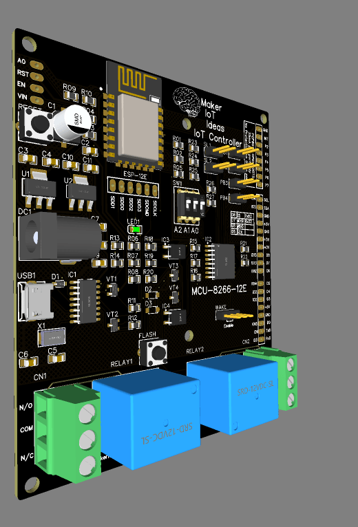
With the initial prototyping of my IoT Controller now completed, and software performing as expected, I have started with the development of an add-on shield. The base device offers 2 built-in relays, and access to another 6 IO Ports on the PCF8574, as well as all the GPIO on the ESP-12E. This is all good and well and suits my initial purposes well, but
I do however now see a need to add more sensors to the device, as well as find an elegant way to power it directly from mains power, while not having lots of wires going anywhere.
So the next steps will be:
Design an add-on-shield to provide me with the following: – Analog inputs. The ESP-12E has only one, and that will be very limiting in some situations. -Digital Inputs and Outputs While there are still unused GPIO ports on the existing board, native to the ESP-12E, having the ability to connect additional devices and sensors will definitely be a good option to have in future. -Some sort of Display Small OLED I2C displays are cheap and easy to use. I can also go full colour with an SPI display…
From here on, I have to decide on how and what. I can go the discreet chip route, by using dedicated I2C chips that provide all these functions, or I can add a secondary micro-controller to the shield, which would provide more flexibility, but can also add complexity to the final design…
Please follow along and join me on the next part of this design journey. I can not promise anything yet, but I do guarantee that it will be exciting…
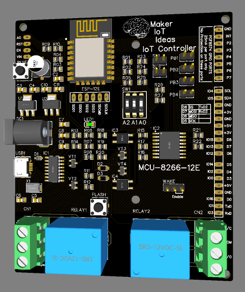
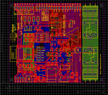
Welcome to Part 3 of this build. If you are new to this series, Part1 and Part2 can be found by clicking on the respective links. Today, we will look at the completed PCB for our IoT Controller. Full disclosure, There are some issues, ranging from components that have still (15 days after being ordered, not been delivered), as well as 3 minor errors on the PCB ( That is entirely my fault ). We will look at how I have overcome the problems to still end up with a functionals PCB. Please note that the errors in the PCB Artwork have BEEN CORRECTED and that the version for public download does not contain any errors. You can thus order it with confidence.
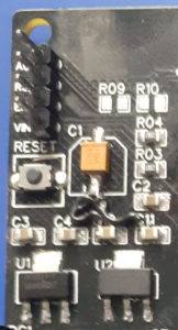
During the design phase, I have forgotten to add a ground to the 5v regulator, and its supporting smoothing capacitors. These components were not initially included in my design, but, while added in later after I decided that since I will be designing the PCB to operate from many different voltage inputs, a reliable 5v source that is not dependent on USB power should be added… The components were added to the schematic, and I forgot to add the ground. It went undetected on the PCB design, as the Ground plane is a copper area…
In the picture above, you can see that I have temporarily fixed it with two wire links from the ground of C1, to the grounds of C10 and C11 respectively. These grounds connect back to U2.
C1 is another issue. Originally designed as a 100uf Electrolytic capacitor, I had to settle for a 10uf Tantalum. The reason being that the ordered capacitors are still floating in logistics space… with no definite ETA.
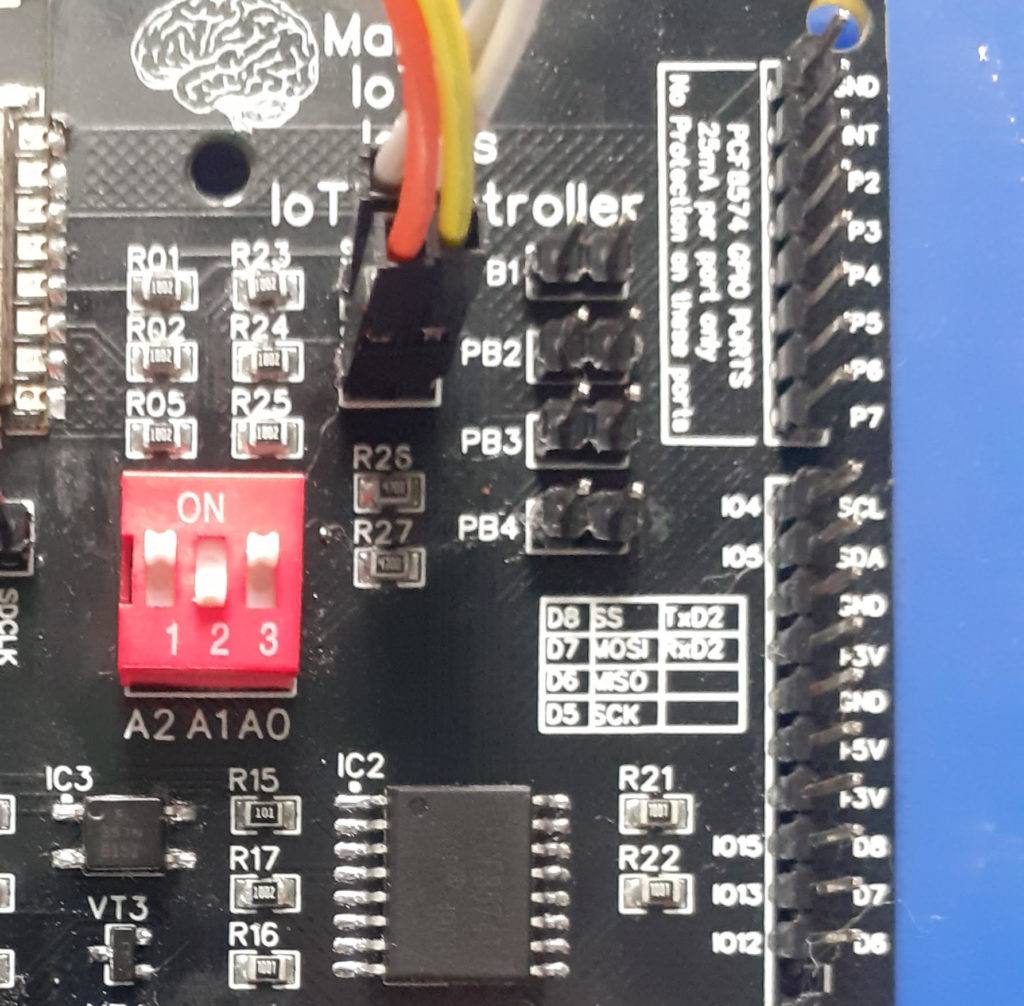
Error on I2C labelling, as well as I2C Pins at IC2
The following error was not so easy to spot. It gave me quite a headache to find. As I normally use netlabels on all the pins of any IC that I use, I have correctly labelled ESP12-E GPIO5 as SCL and GPIO4 as SDA. These netlabels were then transferred onto the PFC8574’s pins but in reverse! Note to self: Always re-read the pinout in the datasheet! To make matters worse, I flipped the SCL and SDA labels on the pin header…
How to fix: I am fortunate that the ESP12-E, like all other ESP Modules, does not have fixed I2C pins. If this was an Atmega based project, the boards would have been useless if tracks could not be cut and reconnected! On the ESP12-E, I2C is however software allocated to any desired GPIO pin. It was thus easily fixed by just swapping the two pins in software.
The third problem encountered is another logistics issue. This is in the process of being resolved, but, as you will soon see, is not actually a problem at all…
I have added support for an onboard USB to Serial converter, via a CH340G chip. The chip requires a 12Mhz resonator or crystal. My dear supplier accidentally sent me an 8 Mhz version. I have thus decided to depopulate the entire USB to Serial circuit, leaving just the USB Port and protection diode on the board. (To allow for powering via USB).
This does mean that programming the board becomes a little more complicated, connecting an external USB to Serial Adapter, and pressing and holding the flash button while pressing and releasing reset for each upload, followed by a manual reset afterwards. This is a pain, but, as I will be using these boards with ESPHome, only required once. All future uploads will be OTA anyway, and the correct components can be retrofitted when they arrive at a later stage.
Powering on the PCB
The PCB was first powered on with an external USB to serial converter and using the Arduino IDE, a simple sketch testing the I2C addressing of the chip, as well as the functioning of all onboard relays and LEDs.
The board was then flashed with ESPHome, using the procedure described in Part 1. I then proceeded to measure the current required by the board, to make sure that it is as designed.
Current Requirements Powered from 9V to 12V DC via the DC Barrel Connector
Standby, Wifi Connected to Home Assistant, All relays and LEDs off 75mA All relays energised, status LEDs all on 255mA
Integrating and Testing with EspHome and Home Assistant
The configuration for ESPHome was updated and uploaded to the device OTA. I decided to add a monitor for the VCC input of the ESP12-E, a remote Restart button, and an external DHT11 Temperature and Humidity sensor. The updated code is available below
esphome:
  name: iot-controller-8266-01
  platform: ESP8266
  board: nodemcuv2

# Enable logging
logger:

# Enable Home Assistant API
api:

ota:
  password: "2f8a73f47f1893f3f7baa391c4d0ba96"

wifi:
  ssid: "<your ssid>"
  password: "<your password>"

  # Enable fallback hotspot (captive portal) in case wifi connection fails
  ap:
    ssid: "Iot-Controller-8266-01"
    password: "y4aaH7vMITsC"

captive_portal:
#--- DO NOT COPY ANYTHING ABOVE THIS LINE ---

# when using this, you need to reassign the status LED to another GPIO
#deep_sleep:
#  run_duration: 5min
#  sleep_duration: 2min

i2c:
  sda: GPIO5
  scl: GPIO4
  scan: true
  id: i2c_bus_a

pcf8574:
  - id: 'pcf8574_hub'
    address: 0x22
    pcf8575: false

status_led:
    pin:
      number: GPIO16
      inverted: true
# Reassign this LED to another GPIO when using deep sleep mode !

sensor:
# Monitor VCC on the ESP12-E
  - platform: adc
    pin: VCC
    name: "Device Input Voltage"
    unit_of_measurement: "V"
# Monitor the WiFi Signal Strength at the device
  - platform: wifi_signal
    name: "WiFi Signal Sensor"
    unit_of_measurement: "dBm"
    update_interval: 240s
# Add Temperature and Humidity Sensor
  - platform: dht
    pin: GPIO2
    temperature:
      name: "Room Temperature"
      unit_of_measurement: "°C"
      icon: "mdi:temperature"
      device_class: "temperature"
      state_class: "measurement"
      accuracy_decimals: 2

    humidity:
      name: "Room Humidity"
      unit_of_measurement: "%"
      icon: "mdi:water-percent"
      device_class: "humidity"
      state_class: "measurement"
      accuracy_decimals: 2
    update_interval: 60s

# Outputs to control relays and led's

output:
 - platform: gpio
   id: relay_1
   pin:
      pcf8574: pcf8574_hub
      number: 0
      mode: OUTPUT
      inverted: true
 - platform: gpio
   id: relay_2
   pin:
      pcf8574: pcf8574_hub
      number: 1
      mode: OUTPUT
      inverted: true
 - platform: gpio
   id: led_status_1
   pin:
      pcf8574: pcf8574_hub
      number: 2
      mode: OUTPUT
      inverted: true
 - platform: gpio
   id: led_status_2
   pin:
      pcf8574: pcf8574_hub
      number: 3
      mode: OUTPUT
      inverted: true
# Monitor the two local control pushbuttons on the device
binary_sensor:
  -  platform: gpio
     id: push_button_1
     name: 'Relay1 Pushbutton'
     device_class: ''
     pin:
        pcf8574:  pcf8574_hub
        number: 4
        mode: INPUT
        inverted: true
     on_press:
      then:
        - switch.toggle: switch_relay1
     filters:
       -  delayed_on_off: 50ms

  -  platform: gpio
     id: push_button_2
     name: 'Relay2 Pushbutton'
     device_class: ''
     pin:
        pcf8574:  pcf8574_hub
        number: 5
        mode: INPUT
        inverted: true
     on_press:
      #min_length: 50ms
      #max_length: 500ms
      then:
        - switch.toggle: switch_relay2
     filters:
       -  delayed_on_off: 50ms

# Allow control from inside Home Assistant

switch:
  - platform: output
    id: switch_relay1
    name: "Relay No. 1 (#0)"
    output: relay_1
    on_turn_on:
    - output.turn_on: led_status_1
    on_turn_off:
    - output.turn_off: led_status_1
  - platform: output
    id: switch_relay2
    name: "Relay No. 2 (#1)"
    output: relay_2
    on_turn_on:
    - output.turn_on: led_status_2
    on_turn_off:
    - output.turn_off: led_status_2
 # Add a remote Reboot switch
  - platform: restart
    name: "Reboot Me"
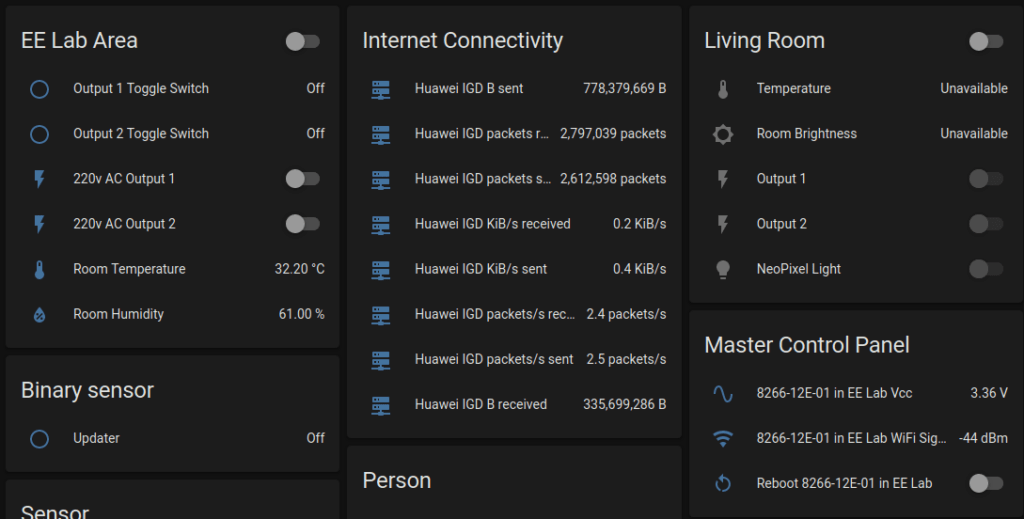
After uploading this configuration, Home Assistant was configured to reflect the changes.
Home Assistant showing the IoT Controller status ( EE Lab Area ) as well as Admin stats (Master Control Panel)
I have decided to split the different status and control outputs from the device into two cards, One in the EE Lab Area, which will later be moved into the actual room(s) where the device will be deployed, as well as on a Master Control Panel. From here, I can reboot individual devices, see their voltages and WiFi Status
Tasmota
As promised before, I did test the device with Tasmota. I had to do a custom compile to get support for the PCF8574. Performance was however VERY poor. ESPHome is snappy and quick, even in local mode. Tasmota seemed to have at least a one-second delay on doing anything. I thus abandoned it, and won’t be making use of it in this project anymore. The flexibility of ESPHome to do what I want, how I want it, is definitely missing in Tasmota. Hopefully, that will change in the future?
Order this PCB for yourself
You can order this PCB from PCBWay as a shared Project, by clicking here. New users will get a $5 USD coupon for use with their first order if they follow the link below to sign up for an account.
I would also like to thank Wendy at PCBWay for once again being a star. The project went smoothly and was very well produced. Make sure to consider using PCBWay for your next PCB order.
Conclusion and further steps
I am in the process of building and assembling another 2 of these devices. I have also ordered and received PolyCarbonate enclosures to mount them in. As this is an ongoing project, I still plan to add I2C temperature measurement chips to each, to measure the temperature inside the enclosure. An Air quality sensor, as well as a CO2 sensor, is also planned, with a possible Display Shield to provide test output locally at the device. This display, at the moment at least, is planned as an I2C Oled or similar. There are also plans to do an option to directly power the unit from 220V AC via an additional base-board for now, or a complete redesign, incorporating everything on one board. Thank you for following along, I hope that you found it educational and entertaining. Please consider joining us on Patreon. We are in the process of creating exclusive content for that platform, as well as for http://144.126.248.244. Most of the content will also remain free for all as usual.
The Internet of Things (IoT), as well as Home Automation, are steadily gaining popularity all the time. You can already buy quite a lot of commercial products or do your own D.I.Y implementation. Many different companies offer various devices and modules to help you do your project easily. But many of us will know that these modules always come with a lot of wires and connections, which can be very unreliable, and also unsightly to look at.
Most of these solutions are also relying on you placing some stuff on an electronics-breadboard, or strip-board for more permanent installations. You can also decide to design and manufacture your own custom PCB.
On the software side of this problem, there are many commercial and open-source solutions available, and most of them work with almost anything on the market (With various degrees of complexity and a varying learning curve).
Having access to a few ( four to be exact ) Raspberry Pi Computers, as well as a huge number of ESP8266, ESP32, Arduino and STM32 Development boards that are lying around in my working area, as well as being quite lazy to do repetitive tasks, I have been playing with the idea for quite a while to automate some or maybe all of the lights in my house. I have also built quite a few device prototypes, only to tear them down again after testing them.
The reason for this, and this is only my own opinion, is that an electronics breadboard is meant for prototyping only. They are not reliable in the long term, and they look extremely messy. Using a certain development board, and connecting all of the supporting components and modules to it, also leaves quite a mess. So,
1) The project must be contained on a single PCB. 2) It must have WiFi and or Bluetooth support (ESP8266 does not have this [ Bluetooth ]) 3) It must be able to be powered from 220v mains directly, OR, through a single Plug Type AC to DC converter, preferably something already available on the market. 4) The power supply unit must supply adequate power to the unit. 5) I want to make some actual use of a Raspberry Pi, as they were not meant to lie around gathering dust 🙂
6) Once completed, the project should be able to be updated OTA or with as little fuss as possible. 7) The freedom to code in whatever language I want, as well as be easy to use with prebuilt firmware like ESPHome and or Tasmota and the likes.
Taking into consideration cost, as well as flexibility, I decided on using the ESP8266 and in later versions ESP32. These have WiFi and Bluetooth already built-in but have a nasty breadboard form factor. The popular NodeMCU is a great starting point, but it has many small design flaws, most of which were fixed in later versions, but, as I live in SE Asia, and electronics are super cheap, you never know what you get.
With this in mind, I have decided to design my own controller, based on the ESP-8266 12E Module. This will give me the flexibility I need while allowing me to add custom components and features as needed, which is not possible with a stock version.
As far as Software is concerned, Home Assistant, running on a Raspberry Pi 4B with 4Gb Ram will be sufficient to control all of this. Firmware on the ESP12-E can be either ESPHome, Tasmota, or something that I write on my own, connecting to the internet and using MQTT for communication. (The options here are also almost too many to mention, but, IFTTT, Adafruit IO, and Blynx come to mind… Alexa and Google Assistant support are also possible, but definitely not required in my application at this moment.
Any permanent project grows on you, and over time, you will want to add features and functions. Keeping this in mind when you start designing saves a lot of headaches later. I will thus definitely make sure to provide access to the I2S, SPI and Serial Peripherals.
Prototyping and Initial Testing
Software It is quite impossible to design something without building a prototype, and doing some very rigorous testing. To do this, I have started with a copy of Home Assistant running in a VM on my HP ML350G Debian server computer. This way, I can quickly test Home Assistant, and make sure everything works as I want it to, without having to do it on the PI. This will mean that I will have to re-do most of the software configuration again on the PI, but it gives me the flexibility to take snapshots and restore them if something goes wrong.
The procedure that I followed, for VirtualBox, can be found here. I am sure that it will be very similar for Windows users.
Start Home Assistant
When you have completed the installation, you can go ahead and start Home Assistant.
You may now open Home Assistant in your browser by going to http://<your-ip-address>:8123 and pressing enter. You will see something similar to this:
Install ESPHome
You may now scroll down to the Supervisor Menu Item, Click on the Addon Store link, and Install ESPHome.
Please make sure that you select “start on boot”, “watchdog”, “auto-update” and “show in the sidebar” Also, make sure to start the add-on
You are now ready to flash ESPHome onto your development board. Please note that you will have to repeat this step on the actual PCB device that we will design and build later. For now, we will however use a standard NodeMCU v3 module, as it contains the ESP-12E module that we require.
As we have not configured HTTPS in our Home Assistant installation, we can only flash the initial firmware using an external application. This application is called ESPHome Flasher, and you can download it here.
Prepare to Flash
We need to create an initial device in ESPHome. to do this, you need to click on the ESPHome Menu Item in the Home Assistant sidebar. Then click on the Green and White + sign at the bottom right corner…
Give your device a descriptive name, I went with iot-con-prototype. Also, add your WiFi network credentials (SSID and Password). Then click on NEXT.
You now have to select your ESP board. I went with NodeMCU.
Click on NEXT when you are done. You will now be alerted that a configuration has been created. Click on the Close button.
You will now see your device in the list. The red line means that the device is OFFLINE.
If you have not installed ESPHome Flasher yet, now is a good time to do it. When you are done, connect the NodeMCU module to the computer’s USB port and start ESPHome Flasher. Note: On Linux, you dont have to install it. you can just start it from the terminal using ./ESPHome-Flasher-1.3.0-Ubuntu-x64.exec ( this example is for Debian ) yours may differ … sudo may be required
Select the communications port from the dropdown menu. Now go back to Home Assistant, ESPHome Screen. Click on the Install link (in yellow) of the device that we added previously. Then click on Manual Download
ESPHome will now compile your initial firmware and prompt you to save the .bin file it has generated.
Take note of the location of this file, we will need it for the next step.
Now you can go back to the ESPHome Flasher window, and browse to the .bin file that you have just generated and downloaded.
When this is done, you can click on Flash ESP. The firmware will now be flashed onto the NodeMCU device that we will use as our prototype.
You can close the Flasher application when you see predominantly purple text in the console window. This means that the device has connected successfully with your WiFi network, and by extension, also with ESPHome and Home Assistant.
If you now go back to ESPHome, you will see that the device has a green line above its name, which means that it is online. Please note that at this stage, the device does not do anything, as we have not yet configured it. That will be our next task, but before we do that, we will have to start playing with some of the physical hardware yet.
Designing the Hardware
I have decided to base this controller on the popular NodeMCU v3 development board. This little board makes use of the ESP12-E module, designed by AITinker, from whom I have bought many well-designed modules before. The module (NodeMCU) is in a BreadBoard form factor, and thus clearly meant for prototyping, or use on a base-board of some kind. I do however have some issues with this module, namely:
1. Many of these units are in fact clones. Some of these does not have proper protection between the board and the USB port to power them. This makes it dangerous to connect power to the VIN pin. 2. The board does not have a built-in 5v regulator. The 5v output (VIN) is thus taken directly from the USB port that powers it. This limits the total available current to the board and all peripherals to the 500mA available from the USB port.
All of these issues are however easy to overcome, as Espressif has made available excellent documentation on using their modules. I will thus be using this documentation as a reference design for my own device.
Another issue is expandability. The module provides many broken out GPIO pins (D0 to D8), but in order to remain super flexible for future expansion, I would have to make sure that I keep the built-in peripherals, like i2c, spi, and uart free for connection to external addon components in future. To solve this, I have decided on using the PCF8574 I2C IO Expander. This means that…
D0 (GPIO16) needs to be kept free for Wake up from deep sleep mode D1 (GPIO5) SCL line of I2C Bus D2 (GPIO4) SDA line of I2C Bus D3 (GPIO0) connected to Flash Button, and also a strapping pin D4 (GPIO2) Tx of UART 1 D5 (GPIO14) HSCLK – SPI Clock D6 (GPIO12) HMISO – SPI MISO D7 (GPIO13) Rx UART 2 / HMOSI – SPI MOSI D8 (GPIO15) Tx UART 2 / HCS – SPI CS as well as a strapping pin D9 ([Rx] GPIO03) Rx UART 0 D10 ([Tx] GPIO01) Tx UART 0
Looking at this, it is thus very clear that I2C is the way to go, as it will use only two pins, leaving the other GPIO’s free for future expansion.
Relay Driver Circuit, status led(s) and user control
The PCF8574 has very weak current sourcing capabilities, but it can sink 25mA per IO pin. As I will be driving the chip from 3v, this will however not be enough to drive a 5v relay. I will thus be making use of an optocoupler to drive the relay from 5v, using a general-purpose NPN transistor. That way, I can make sure that I do not overload the IO line on the PCF8574, as well as keep the 3v and 5v lines isolated from each other. (They will however still share a common ground).
Relay Driver Schematic
As you can see from the schematic above, the relay driver(s) will be connected to P0 and P1 of the PCF8574. A 200-ohm resistor will limit the current to about 16.5mA @ 3.3v. This is well within the tolerance of 25mA for the PCF8574 as well as the 50mA limit of the EL357N Optocoupler chip.
On the output side, I made use of the S8050 general purpose NPN transistor, capable of a 25v collector-emitter voltage, ant a continuous current of 500mA. Move than sufficient to drive the +/- 70mA to 80mA of current required by the relay coil. The current through the phototransistor side of the optocoupler is limited by a 1k resistor to the base of the transistor, to 5mA.
PCF8574 IO Expander Status LED(s) and User Input Schematic
Provision is made for up to four (4) pushbuttons, by pulling pins P4 to P7 down to ground, through an external push-button connected to a 2-way pin header. The design allows for the pin to be used for another function as well, with an additional breakout pin provided on the edge of the board.
Likewise, the two status LED’s on P2 and P3 is connected via a 470-ohm resistor each, driving them at approximately 7mA each. This is once again within the 25mA sink limit of the PCF8574. These pins can also be used to connect to other hardware instead via the breakout header at the edge of the board.
The user input(s) and status led circuit was purposefully kept as plain as possible, as it is very likely that the additional 6 ports taken up by these will be used for other purposes instead.
USB to Serial Interface
The USB-to-Serial interface is done by using a CH340G. I have not modified the reference design from the original NodeMCU v3 too much, as it works well, and thus need no changes. I did however make sure that there is a protection diode between the USB 5v line and the VIN line on the PCB. Most of the existing NodeMCU boards does not do this, or when they do have the protection diode, that line is directly connected to the VIN pin. in my view, that is not ideal, and can cause unnecessary damage to your computer’s USB port or NodeMCU board in the event that you power it from an external source, and also use USB power to upload code… Not that it should be done that way anyway, but rather safe than sorry later.
USB-to-Serial Schematic
The two transistors (VT1, and VT2) is used to do very cleverly put the board into programming mode, as well as reset it after flashing, without the end-user having to press any of the flash or reset buttons. This is also part of the reference design on some of the NodeMCU boards. I can not comment if it is standard. I found it useful, so decided to include it as well.
ESP-12E with strapping pins and power supply
The ESP-12E module, as manufactured by AITinker, seems to be quite stable and easy to use. It does however have a couple of caveats, to enable it to function as intended. The strapping pins (discussed later) should be in a certain state at bootup time, and failure to adhere to that will definitely cause a failed boot or wrong startup mode.
GPIO0, GPIO2, EN and RST should be pulled HIGH for a NORMAL boot, while GPIO15 should be pulled LOW. Pulling GPIO0 LOW at boot, will put the board into FLASH mode.
Another change that I made is that I did not break out the raw Analog input pin, as is done on some of the boards ( as a VV pin, or sometimes as an unlabeled, or reserved pin). The Analog input pin on the stock module is designed for around 1.0v input. This is fed from a resistor divider, to effectively scale your 5v input down to valid levels.
ESP-12E and Power Supply Schematic
GPIO16 (D0) is used internally by the ESP-12E to wake the module from deep sleep. This is done by connecting GPIO16 to the reset pin. To wake up the module, GPIO16 is internally pulled LOW, thereby resetting the module. I have decided to add a user-selectable jumper that can be enabled to connect GPIO16 to RESET, that enabling this functionality. It is however to be noted that the jumper must ONLY be set AFTER the relevant deep sleep mode has been enabled in the firmware for the module.
The standard NodeMCU has only a single 3.3v voltage regulator installed. I added a dedicated 5v voltage regulator as well and powered it directly from the VIN pin. This regulator will only function when the device is powered from an external power source, with an upper voltage limit of 15v DC. Protection for the USB port is provided by a diode between VCC_USB and VCC5V.
As I have mentioned at the start of the article, this is a show and tell, of how I solved a particular problem that I had. I do not believe in re-inventing the wheel, but to adapt and improve as and where I see fit, to my own purpose. This project will by no means be unique, or better or worse than other similar devices on the market today. It is however designed to suit my particular needs for my particular project.
The design of the PCB and Schematics was done in EasyEDA, which I believe to be quick and easy to use, as well as Linux friendly. (There does not seem to be many of those around, KiCAD being the exception to that rule. I have however not been too successful in using that before, to no fault of KiCAD at all. I am just not prepared to learn a new EDA CAD package just for the sake of doing it. Time is precious, and I can get everything I need to do done with EasyEDA).
PCB Layout
The PCB is dual-layer 99.06mm x 83.058mm. Six mounting holes are provided. The ESP-12E is placed at the top, roughly in the left-hand corner. As per Espressif design recommendations, no tracks are routed underneath the antenna area. An approximate 15mm x Board width area is also kept clear of any tracks or ground plane(s) to also prevent interference with the RF signal generated by the device. All components are mounted on the top payer of the PCB and are as far as possible grouped together by their function and purpose in the circuit. As the two onboard relay modules will very likely be used to switch mains power, they have also been excluded from the ground plane(s). Cutouts around all possible mains power carrying pads and tracks were also added to prevent tracking.
A DC Power Socket, and USB port, as well as access to the single Analog Input, Enable, Reset Pin and Button and VIN pin is provided on the left-hand side of the PCB. All other IO pins, as well as the six remaining ports on the PCF8574 IO expander, is accessible on the right. Note that GPIO4 and GPIO5 ( D1 and D2 ) were hard-wired as I2C lines. They should thus not be used for any other purpose. All other pins are accessible and broken out, clearly labelled with their GPIO numbers, as well as NodeMCU style Dx numbers. There are also an additional 6 IO pins broken out at the bottom of the ESP-12E module, to provide access to the seldom-used SDCard interface.
PCB Top Layer ( Rendered )
PCB Bottom Layer (Rendered)
3D Render PCB from Left
Manufacturing the PCB
This PCB will be manufactured at PCBWAY. The Gerber files and BOM, as well as all the schematics, will soon be available as a shared project on their website. If you would like to have PCBWAY manufacture one of your own, designs, or even this particular PCB, you need to do the following… 1) Click on this link 2) Create an account if you have not already got one of your own. If you use the link above, you will also instantly receive a $5USD coupon, which you can use on your first or any other order later. (Disclaimer: I will earn a small referral fee from PCBWay. This referral fee will not affect the cost of your order, nor will you pay any part thereof.) 3) Once you have gone to their website, and created an account, or login with your existing account,
4) Click on PCB Instant Quote
5) If you do not have any very special requirements for your PCB, click on Quick-order PCB
6) Click on Add Gerber File, and select your Gerber file(s) from your computer. Most of your PCB details will now be automatically selected, leaving you to only select the solder mask and silk-screen colour, as well as to remove the order number or not. You can of course fine-tune everything exactly as you want as well.
7) You can also select whether you want an SMD stencil, or have the board assembled after manufacturing. Please note that the assembly service, as well as the cost of your components, ARE NOT included in the initial quoted price. ( The quote will update depending on what options you select ).
8) When you are happy with the options that you have selected, you can click on the Save to Cart Button. From here on, you can go to the top of the screen, click on Cart, and make any payment(s) or use any coupons that you have in your account.
Then just sit back and wait for your new PCB to be delivered to your door via the shipping company that you have selected during checkout.
Conclusion of Part 1
This is the end of a very long part 1. We have started to look at the steps involved to get started with designing our own IoT Controller, did some initial software installation, and took a detailed look at the schematics and PCB…
In part 2, we will look at
1) Writing the configuration for ESPHome to control your device 2) Look at Tasmota as an alternative way to control the device 3) Integrating the device into Home Assistant 4) Have a go at writing our own firmware using the Arduino IDE to control the device using MQTT 5) Depending on how long shipping of the components and PCB takes, assembly and testing of the actual device
Thank you for your time. This is a very long article, and I appreciate your interest.