Breadboard Power Rail Bridge

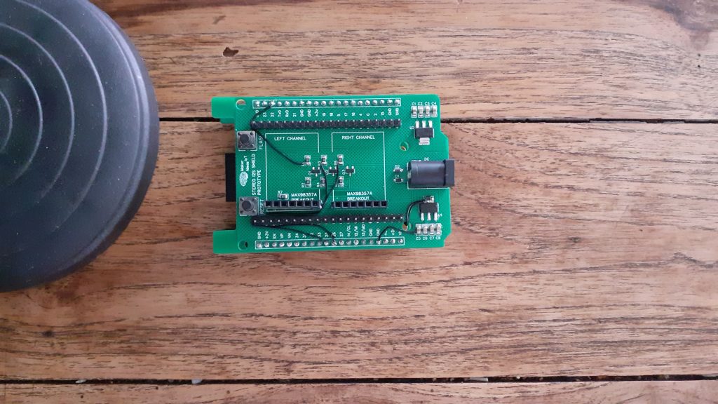
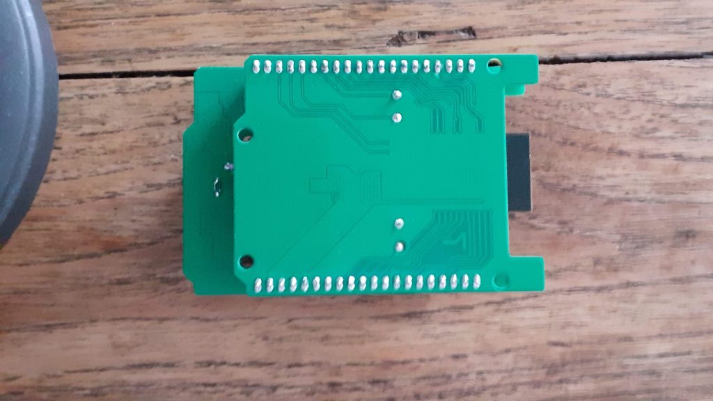
This is a sort of tongue-in-the-cheek project, that started with good intentions, and ended up wholly over-engineered and sort of “broken” due to adding “added features” like LEDs and an additional power header.

What was the initial intention?

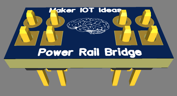
[This is what I actually wanted to achieve]


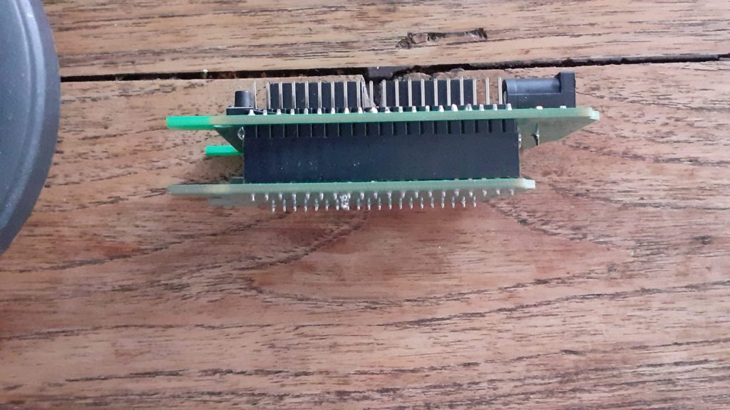
My breadboards all have interrupted power rails, and it is thus always necessary to bridge them with jumper wires to have a continuous rail. This is needed because I very often have more than one project on a single breadboard, and do not want to have to use separate power modules for each. I also tend to test out some part of a circuit on a separate part of the breadboard, before incorporating it into the main circuit.

[ I completely overdesigned this, ending up with something completely different from what I wanted]


Wire jumpers are definitely the easier and fastest, but having been struck by a “what if I do this instead” moment, this tiny PCB was designed and subsequently sent to manufacturing…

So does it work?

Yes, it works, for its intended purpose of bridging the power rails, but that is where the wheels come off. Let me explain, trust me, it will be fun, and we can all laugh at it in the end…

Breadboard power rails are usually marked Red for positive, and Blue or Black for negative… Most people on this planet are also right-handed, and would thus place a power module on the right-hand side of a breadboard ( although some won’t..) Being left-handed myself, and still trying to please right-handed people, my power module will be “upside down” on the left-hand side of a breadboard… which is fine with me, as I remember to swap the colours of the rails in my mind, making red negative and blue positive… not a big issue is you always do it that way…

So what went wrong…

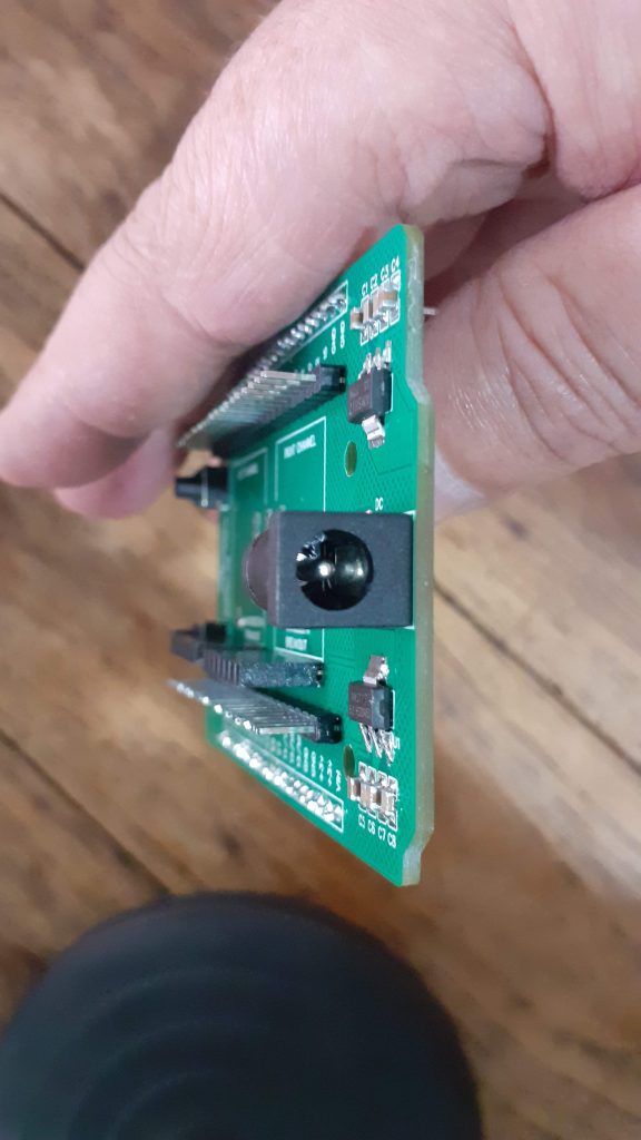
While designing this, I initially planned on a simple PCB bridge, with a jumper on the positive line, acting as a switch, and a continuous ground that is always connected.. all fine, problem number 1 being that I looked at the colours of the power rails while designing it, measuring the gaps etc to get the spacing just right…

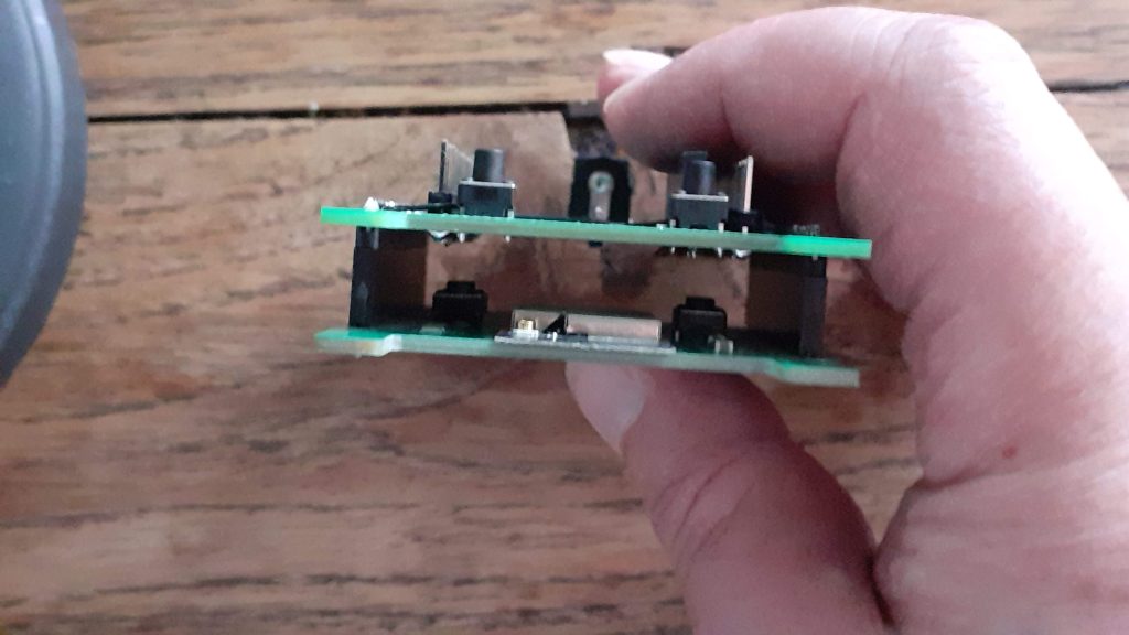
Problem number 2 is that the top and bottom rails are in the same configuration, Red at the top, blue at the bottom… and thus plugging in a bridge into either should be ok… and it really should have been, if I did not decide to add a status LED on each side of the bridge, and an additional power header… because turns out that I forgot that the bridge at the top will in effect be “mirrored” when plugged in ( and thus having components that are reversed polarity) – mirrored, due to the fact that you now have to plug the top rail bridge upside down into the breadboard, because it will otherwise interfere with the prototyping space

[This was the direct effect of my lack of attention to detail – and yes, it works perfectly in this configuration – if we ignore the wasted space on the top half of the board]

[This is the practical reality – one bridge must be installed ‘upside-down’]

Lesson learned; I can be quite scatterbrained at times, especially when juggling a few projects and customers at the same time ( I am only human anyway ). Thus this project, although it looks nice, and can be useful, needs to go back to the drawing board for a complete redesign, without all those “added features”
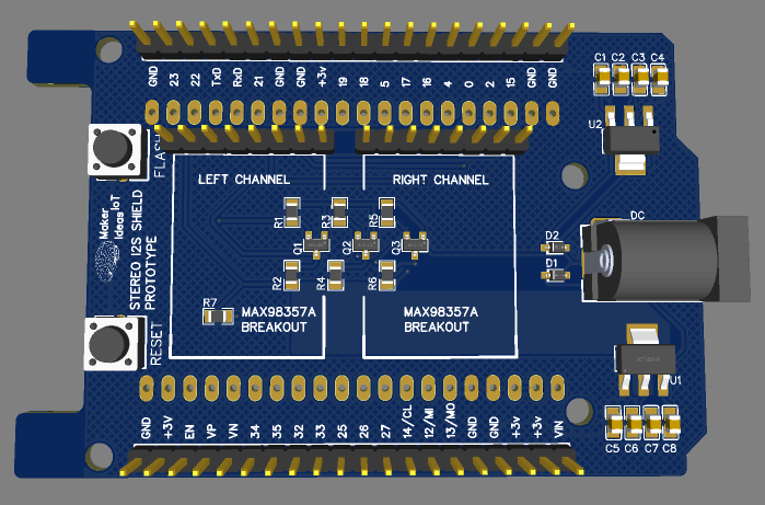
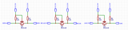
The Schematic


The schematic is straightforward, with no surprises. Two LEDs ( polarity sensitive ) and then those headers and jumpers, which also need up being polarity sensitive – in a manner of speaking

Quite different from what I originally wanted to do

Manufacturing

I choose PCBWay for my PCB manufacturing. Why? What makes them different from the rest?

PCBWay‘s business goal is to be the most professional PCB manufacturer for prototyping and low-volume production work in the world. With more than a decade in the business, they are committed to meeting the needs of their customers from different industries in terms of quality, delivery, cost-effectiveness and any other demanding requests. As one of the most experienced PCB manufacturers and SMT Assemblers in China, they pride themselves to be our (the Makers) best business partners, as well as good friends in every aspect of our PCB manufacturing needs. They strive to make our R&D work easy and hassle-free.

How do they do that?

PCBWay is NOT a broker. That means that they do all manufacturing and assembly themselves, cutting out all the middlemen, and saving us money.

PCBWay’s online quoting system gives a very detailed and accurate picture of all costs upfront, including components and assembly costs. This saves a lot of time and hassle.

PCBWay gives you one-on-one customer support, that answers you in 5 minutes ( from the Website chat ), or by email within a few hours ( from your personal account manager). Issues are really resolved very quickly, not that there are many anyway, but, as we are all human, it is nice to know that when a gremlin rears its head, you have someone to talk to that will do his/her best to resolve your issue as soon as possible.

Find out more here

Conclusion

This project served many purposes beyond the actual use of the PCB that was designed. In a way, I am quite happy that I screwed up so badly on this one – here is the reason why:

Because I do quite a lot of PCB design each month, for customers or personal projects, I often tend to get a bit over-confident, and also rush things through,
while believing that I will catch every mistake before I send something off to production. Normally, I am quite good at that, and my error rate is actually quite low… But, This month, being quite busier than usual, and having had a fair amount of distractions, served as the perfect lesson to drag me down a notch or two, and remind me that I have to be way more attentive, especially when things are going hectic, and there are a few projects to juggle around at the same time.

The second reason why it is a good thing when the wheels come off like this, once in a while, is that it serves as a perfect example of what your PCB manufacturer’s actual job is. So, this is especially for the new guys that may not know this: Your PCB Manufacturer has only one job – To manufacture your PCB EXACTLY AS YOU DESIGNED IT – Scary, right? Sure, they will let you know if your design falls outside of their tolerances of capabilities. They will let you know if your board fails a flying probe test if you have that kind of arrangement with them… But it is NEVER their job to correct or attempt to change any of your design files.

So, what is the moral of the story, regarding both of the points that I made above?

If you screw up on the design, it is your, and only your fault. Nobody else is to blame, ever. The buck stops with you, the designer.

Stereo I2S Shield for ESP32-S Dev Board

Sound or music adds another level of complexity to any project. Having the ability to easily add it as a shield, allows for a reduced level of this complexity, and hopefully stimulates some inspiration along the way.

This was the thought process that inspired this Stereo I2S Shield, for use with my ESP32-S Dev Board. During the design process, and actually, before, many things happened that turned this project into a slightly more complicated task than I have initially accounted for.

The short and sweet is that I made a few silly mistakes on the PCB, which, for the prototype at least, has been fixed with a few jumper wires. [ I have since updated the Gerber files with the correct design, omitting these silly mistakes.]

Let us take a look at what happened.

  1. I forgot the ground connection on the 5v Regulator, and since I placed extensive ground copper pours on both sides of the PCB, I missed that one completely.
  2. I forgot to connect the 5v supply to the Max98357A breakout headers
  3. I also completely forgot to connect any signal traces to these breakouts
  4. The breakouts were placed on the wrong side of the PCB ( if looking top to bottom on the picture below, they should be towards the top)

How does this happen, and most importantly, why would I even mention my mistakes here, in public?

The most important here is that I am human. Humans make mistakes. Rushing through converting a design that works perfectly on a breadboard onto a PCB should not happen, but it does happen, and that is why the first iterations of a PCB are called prototypes. Dealing with customers, while working on a design, as well as life’s other interruptions very often results in small mistakes, which I usually catch before a board goes for manufacturing. In this case, I did not catch them until after I received the board back from the factory.

The other part of this coin is transparency. There are many many projects on the internet, some good, some excellent, and some outright terrible. Without giving a score to any of my own, my only intention is that whatever I present on this medium MUST be completely honest, my own work, and it must work. Any mistakes MUST be made public, regardless of what the public thinks of it afterwards.

With the ranting done now, let’s take a look at the board, which, after fixing the issues, actually works perfectly…

(I will make use of a rendered image showing the repaired PCB, as it will be the least confusing)


In the rendered image above, we can clearly see what it should have looked like, with the MAX98357A breakouts in their correct places, and all power and signal traces connected correctly.

Part of the reason for the mistakes on the initial prototype PCB was that I felt it necessary to add logic-level conversion to the I2S modules. The reason for that is that in order to get a bit more volume out of them, they are powered at 5v.


With the GPIO pins of the ESP32 being 3.3v, I felt that it is not warranted to take a risk and power the I2S breakouts at 5v, and send them 3.3v signals. That sparked the whole issue, with adding my standard Bss138-based logic converter circuit to the mixture.


The board contains its own Flash and Reset buttons, which are slaved to the stacked ESP32-S dev board at the bottom.
Further to that, the board provides a DC barrel connector, which will power the I2S shield, as well as the ESP32-S dev board via its Vin Pin

Since the MAX98357A breakouts seem to pull quite a bit of current ( about 500mA or more each, depending on the volume), the shield has its own voltage regulators. I have found that during the experimentation on the breadboard, the single 3.3v regulator on the ESP32-S Dev board was a bit inadequate to drive two of these modules and the ESP32 as well.

Software and Code

The code for the device is far from perfect at this stage, consisting mainly of example code that was provided by the i2s library, to which I have started making minor changes, the most significant being moving the entire audio process to an alternate core of the ESP32. This was done because the audio process seem to be blocking, and, as I plan to later add controls and displays to this device, that would result in an issue later.

/*
  Simple Internet Radio Demo
  esp32-i2s-simple-radio.ino
  Simple ESP32 I2S radio
  Uses MAX98357 I2S Amplifier Module
  Uses ESP32-audioI2S Library - https://github.com/schreibfaul1/ESP32-audioI2S

  
*/

// Include required libraries

#include "Arduino.h"
#include "WiFi.h"
#include "Audio.h"
#include "ESPmDNS.h"
#include "time.h"


// Define I2S connections
#define I2S_DOUT  22
#define I2S_BCLK  26
#define I2S_LRC   25


// Create audio object
Audio audio;

// Wifi Credentials
String ssid =    "<your ssid here>";
String password = "<your password here>";

void audioTask(void *pvParameters) {
  while(1) {
    audio.loop();
  }
}


void setup() {

  // Start Serial Monitor
  Serial.begin(115200);
  

  // Setup WiFi in Station mode
  WiFi.disconnect();
  WiFi.mode(WIFI_STA);
  WiFi.begin(ssid.c_str(), password.c_str());

  while (WiFi.status() != WL_CONNECTED) {
    delay(500);
    Serial.print(".");
  }

  // WiFi Connected, print IP to serial monitor
  Serial.println("");
  Serial.println("WiFi connected");
  Serial.println("IP address: ");
  Serial.println(WiFi.localIP());
  Serial.println("");

  // Connect MAX98357 I2S Amplifier Module
  audio.setPinout(I2S_BCLK, I2S_LRC, I2S_DOUT);
  
  // Set thevolume (0-100)
  audio.setVolume(10);

  // Connect to an Internet radio station (select one as desired)
  //audio.connecttohost("http://vis.media-ice.musicradio.com/CapitalMP3");
  //audio.connecttohost("mediaserv30.live-nect MAX98357 I2S Amplifier Module
  //audio.connecttohost("www.surfmusic.de/m3u/100-5-das-hitradio,4529.m3u");
  //audio.connecttohost("stream.1a-webradio.de/deutsch/mp3-128/vtuner-1a");
  //audio.connecttohost("www.antenne.de/webradio/antenne.m3u");
  //audio.connecttohost("0n-80s.radionetz.de:8000/0n-70s.mp3");
  //audio.connecttohost("http://live.webhosting4u.gr:1150/stream");
  audio.connecttohost("0n-80s.radionetz.de:8000/");
  disableCore0WDT();
  xTaskCreatePinnedToCore(audioTask,"audiotask",10000,NULL,15,NULL,0);
}


void loop()

{
  // Run audio player
  //audio.loop();
 
}


//

// Audio status functions

void audio_info(const char *info) {
  Serial.print("info        "); Serial.println(info);
}
void audio_id3data(const char *info) { //id3 metadata
  Serial.print("id3data     "); Serial.println(info);
}
void audio_eof_mp3(const char *info) { //end of file
  Serial.print("eof_mp3     "); Serial.println(info);
}
void audio_showstation(const char *info) {
  Serial.print("station     "); Serial.println(info);
}
void audio_showstreaminfo(const char *info) {
  Serial.print("streaminfo  "); Serial.println(info);
}
void audio_showstreamtitle(const char *info) {
  Serial.print("streamtitle "); Serial.println(info);
}
void audio_bitrate(const char *info) {
  Serial.print("bitrate     "); Serial.println(info);
}
void audio_commercial(const char *info) { //duration in sec
  Serial.print("commercial  "); Serial.println(info);
}
void audio_icyurl(const char *info) { //homepage
  Serial.print("icyurl      "); Serial.println(info);
}
void audio_lasthost(const char *info) { //stream URL played
  Serial.print("lasthost    "); Serial.println(info);
}
void audio_eof_speech(const char *info) {
  Serial.print("eof_speech  "); Serial.println(info);
}

Important parts of the code to note are as follows

disableCore0WDT();
  xTaskCreatePinnedToCore(audioTask,"audiotask",10000,NULL,15,NULL,0);

This code disables the Watchdog Timer on Core0 of the ESP32, as well as creates the audio task, which is defined earlier in the code

void audioTask(void *pvParameters) {
  while(1) {
    audio.loop();
  }
}

It is also important to note that the loop() in the code is essentially empty, with all code commented out. As mentioned above, I do plan to add additional functionality later, and in that case, there will either be other tasks running, or be some code in the main loop.

Another VERY important issue is the DOUT pin, which I have defined as GPIO22.
This pin is usually used as an I2C pin, but it seems that the I2S hardware on the ESP32-S does not like running the DOUT signal on another pin. This is not an issue, as you can assign another pin to I2C without any issue if you need to use that as well.

Manufacturing

I choose PCBWay for my PCB manufacturing. Why? What makes them different from the rest?

PCBWay‘s business goal is to be the most professional PCB manufacturer for prototyping and low-volume production work in the world. With more than a decade in the business, they are committed to meeting the needs of their customers from different industries in terms of quality, delivery, cost-effectiveness and any other demanding requests. As one of the most experienced PCB manufacturers and SMT Assemblers in China, they pride themselves to be our (the Makers) best business partners, as well as good friends in every aspect of our PCB manufacturing needs. They strive to make our R&D work easy and hassle-free.

How do they do that?

PCBWay is NOT a broker. That means that they do all manufacturing and assembly themselves, cutting out all the middlemen, and saving us money.

PCBWay’s online quoting system gives a very detailed and accurate picture of all costs upfront, including components and assembly costs. This saves a lot of time and hassle.

PCBWay gives you one-on-one customer support, that answers you in 5 minutes ( from the Website chat ), or by email within a few hours ( from your personal account manager). Issues are really resolved very quickly, not that there are many anyway, but, as we are all human, it is nice to know that when a gremlin rears its head, you have someone to talk to that will do his/her best to resolve your issue as soon as possible.

Find out more here

Assembly

Assembly was straightforward, with no issues, as all of the components can quite easily be soldered using a standard soldering iron, or hot air. This PCB does not require a stencil, but, you can of course have one made if you want to.

As mentioned in the introduction, I had to do a lot of after-assembly-hacking to get the board to work correctly. This will however not be needed with the second-generation PCB, as I have already fixed all those issues on the Gerber files.

Picture Gallery

Low BOM cost 4-cell 18650 Charger

Due to their high capacity and relatively low cost, LiPo cells are almost everywhere these days. This Low BOM cost 4-cell 18650 Charger module is my attempt to solve another issue.

The 18650 Lipo cell is quite common in my lab, and for an excellent reason, as mentioned above, they are cost-effective and also store quite a bit of energy. recharging them after use has however been quite a lengthy exercise in the past.

The usual process involved a few Lipo Charging modules, all connected via USB cables, charging one cell at a time. This not only takes up quite a bit of time and space but also occupies USB ports that could be used for other purposes.

Based on the ultra-cheap TP4056 chip, these single-cell charging modules cost peanuts, but with the required wiring and battery holders, as well as the cables to supply power, it does not really look very neat. I have thus been looking for a better solution for quite a while now, and had quite a few requirements for my “ideal” module.

The MCP73832 from MICROCHIP seemed like a good choice for a custom design, as it requires only 5 additional external components, which are only two resistors, two capacitors and an led. The chip is also extremely low-cost.

  • High accuracy preset output voltage regulation (+/-0.75%)
  • Output voltage options include 4.2V, 4.35V, 4.4V and 4.5V
  • User-programmable charge current
  • Open-drain status output
  • On-chip thermal regulation
  • Preconditioning and end-of-charge ratio options
  • Under-voltage lockout

Includes integrated pass transistor, integrated current sensing, and reverse discharge protection in 5-pin SOT-23 and thermally-efficient 8-pin 2mm x 3mm DFN packages.

The Prototype Module


The design that I came up with, can charge 4-cell simultaneously. The maximum input voltage is limited to 6v DC.


Another interesting feature is the ability to use either through-hole battery holders or SMD ones. I did that because I have quite a few of the through-hole ones in stock, but as they were bought quite a while ago, the exact part number went on holiday. When having the module assembled in the factory,the SMD parts can be used, as there seems to be plenty in stock.

The Schematic

Because I enjoy a challenge, the design uses the smaller 3mm 2mm DFN8 package. Charging current is set with R9, which is 2k in this case, which will result in a charging current of the full 500mA. You can adjust it as per your requirements, to a value between 2k and 10k, as per the datasheet.

The full schematic is available here:

PCB Design

The PCB design was optimised to fit on a 10cm x 10cm board. Most of the board is made up of a solid copper pour to provide a good ground plane. Charging circuitry is placed as close together as possible, with a good connection of the thermal pad on the DFN8 package to the ground plane to help with thermal regulation. In this case, I have attempted to replicate the suggested reference design as closely as possible, while adapting it for use with the DFN8 package (Reference design uses the 5 lead SOT-23 package)


As seen in the close-up, components are placed as close as possible to the MCP73832, and via stitching are used to ensure a good connection to the ground, as well as allow the ground plane to serve as a heatsink.

Manufacturing

I choose PCBWay for my PCB manufacturing. Why? What makes them different from the rest?

PCBWay‘s business goal is to be the most professional PCB manufacturer for prototyping and low-volume production work in the world. With more than a decade in the business, they are committed to meeting the needs of their customers from different industries in terms of quality, delivery, cost-effectiveness and any other demanding requests. As one of the most experienced PCB manufacturers and SMT Assemblers in China, they pride themselves to be our (the Makers) best business partners, as well as good friends in every aspect of our PCB manufacturing needs. They strive to make our R&D work easy and hassle-free.

How do they do that?

PCBWay is NOT a broker. That means that they do all manufacturing and assembly themselves, cutting out all the middlemen, and saving us money.

PCBWay’s online quoting system gives a very detailed and accurate picture of all costs upfront, including components and assembly costs. This saves a lot of time and hassle.

PCBWay gives you one-on-one customer support, that answers you in 5 minutes ( from the Website chat ), or by email within a few hours ( from your personal account manager). Issues are really resolved very quickly, not that there are many anyway, but, as we are all human, it is nice to know that when a gremlin rears its head, you have someone to talk to that will do his/her best to resolve your issue as soon as possible.

Find out more here

Assembly

Assembly of this module definitely requires the use of a stencil. The DFN-8 package of the IC is only 3mm x 2mm, and there are 8 leads as well as a thermal pad crammed in there. A stencil will ensure that you add just the correct amount of solder paste to each pad.


As we can clearly see in this cropped picture of the stencil, those pads are SUPER tiny.

I chose to use the hotplate, as well as some hot air for the SMD component assembly. The battery holders and DC barrel-connector are all through-hole, and were thus assembled using a standard soldering iron, with slightly thicker solder, and a bit more heat than normal, as the pads are quite big, and the big copper pour really sucks the heat away from the joints.

Testing

Testing the module went really well. I used four 18650 cells that needed recharging, and they were very quickly ( in about 1 hour ) charged to 4.20 volt.

The Charge Indicator LED on each charging circuit works in reverse from what we would normally expect, with it lighting up while charging, and going out when done.

The current draw (measured on the bench power supply) verified that each cell was charging at the 500mA as designed. The current draw also reduced as each cell charging cycle completed and eventually went down to very close to zero (The Ampere meter on my bench supply can not measure very low current with a lof of accuracy -:) )

Measuring each cell that have completed its charging cycle with a standard multimeter confirmed that they were indeed at 4.20v, and that the charging circuitry was no longer feeding current to any of them.

Drawing current out of a single cell (I used a set of clips ) to power a dummy load, resulted in an automatic recharge cycle being initiated once the cell voltage dropped past the set charging threshold.

It is however VERY important to note that this module is by NO means a balanced cell charger. It is a 4-way single cell charger that charges 4 cells independently from each other, at the same time. It is thus completely possible as well as probable that the four cells will/may be at slightly different voltages at the end of each respective charging cycle.

Conclusion

This project is most definitely high on the list of my most needed items. Keeping a bunch of 18650 cells charged and correctly maintained can be quite a chore, and the way that I have done it in the past was definitively not ideal.
It has also cost me quite a few cells that died way before their time.

Using this module, the chore of charging these cells will be reduced by a lot, and hopefully, in the future, I will come up with a solution to augment this module so that I can have these cells on a semi-permanent charge, with monitoring and only charging those cells that needs it.

Pictures

Variable Breadboard Power Module

A few weeks ago, I designed and built my own breadboard power module, mainly to try and solve some perceived problems with commercial ones, and also just to have something that is completely my own.

While that design does indeed work very well, I did however find a few tiny issues that still needed attention.

  • Two fixed voltages, 3.3v and 5.0v
  • 1A current limit per regulator
  • PCB Heatsink design can be improved further, as there is still a bit too much heat at a high current draw – not much actually, but I like things running as cool as possible.

Other requirements that popped up were the ability to have more than two set voltages, as well as being able to send the full Vsupply to a power rail if I choose to do so…

Having a few LM317G variable voltage regulators lying around, left over from a previous project, I decided to use those. They can source an additional 500mA of current (1500mA in total) and also makes it quite easy to have variable voltages.

Voltage is set with two resistors, of which one is usually a variable resistor. This does however mean that you need a multimeter or other device capable of measuring voltage each time that you need a different voltage, as well as to determine at what voltage the device is currently set if you have not used it in a while…

The initial prototype is quite bulky at the moment, but I do plan to change that in the future when I am completely happy with the performance of the module

Each “voltage channel” consists of a 5k multiturn “trim pot” that connects back through a selectable jumper to a 240-ohm resistor ( I actually used two precision 120-ohm resistors in series) on the adjust pin of the regulator.

I have also reduced the number of smoothing capacitors on the input and outputs, as the voltages are quite stable

After assembly, it only takes a few minutes to adjust each “trim pot” to the correct value using a small screwdriver and a multimeter. Once set and verified, they can be locked using a drop of “lock-tight” or similar.

The eight “trim pots” sets the voltages as follows:

Top Rail:
VR1 – 3.3v
VR2 – 5.0v
VR3 – 7.2v
VR4 – 9.0v

Bottom Rail:
VR5 – 3.3v
VR6 – 5.0v
VR7 – 7.2v
VR8 – 9.0v

Turning the “pot” anti-clockwise reduces the voltage, while a clockwise movement increases it.

Changing voltages then becomes as easy as changing a jumper to a preset position.

The Schematic


As mentioned above, I have used two precision 120-ohm resistors on one leg of the resister divider that is connected to the adjust leg. Feel free to replace that with a single 240-ohm resistor and a 0-ohm bridge.

The multiturn precision 5k trim pots give great control and the desired voltages can be dialled in very accurately.

The module was designed as a double-layer PCB. I used big solid ground planes to provide good grounding, as well as serve as heat sinks for the voltage regulators.


Manufacturing

I choose PCBWay for my PCB manufacturing. Why? What makes them different from the rest?

PCBWay‘s business goal is to be the most professional PCB manufacturer for prototyping and low-volume production work in the world. With more than a decade in the business, they are committed to meeting the needs of their customers from different industries in terms of quality, delivery, cost-effectiveness and any other demanding requests. As one of the most experienced PCB manufacturers and SMT Assemblers in China, they pride themselves to be our (the Makers) best business partners, as well as good friends in every aspect of our PCB manufacturing needs. They strive to make our R&D work easy and hassle-free.

How do they do that?

PCBWay is NOT a broker. That means that they do all manufacturing and assembly themselves, cutting out all the middlemen, and saving us money.

PCBWay’s online quoting system gives a very detailed and accurate picture of all costs upfront, including components and assembly costs. This saves a lot of time and hassle.

PCBWay gives you one-on-one customer support, that answers you in 5 minutes ( from the Website chat ), or by email within a few hours ( from your personal account manager). Issues are really resolved very quickly, not that there are many anyway, but, as we are all human, it is nice to know that when a gremlin rears its head, you have someone to talk to that will do his/her best to resolve your issue as soon as possible.

Find out more here

Assembly

The assembly of this module is quite easy, no stencil is required. I recommend that you take care of the SMD components first, using hot -air or even hand soldering them, before assembling the through-hole components.

Here I do recommend that you use a breadboard to make sure that the 2.54mm headers that will connect to the power rails are lined up nicely

Testing and Setup

As already described above, the module does require a bit of setup after assembly. To do this, you will require a DC power supply with a voltage of 7v to 12v, as well as a multimeter, preferably with clips on the test leads, as well as a small terminal screwdriver.

  • With the module powered, and the Rail Voltage jumpers set to VCC, measure the rail outputs with the multimeter ( remember that the rail active jumper MUST be set to on). Both rails should be at the same voltage as your VCC input voltage, ie 12v DC
  • Move the Select Voltage jumper for both rails to the 3.3v position, and the Rail voltage jumper to the VSelect position for both rails.
  • With the multimeter connected to each rail in turn, turn VR1 anti-clockwise until the voltage for the top rail is set to 3.3v. Repeat for the bottom rail, adjusting VR5 instead, while measuring the bottom rail.
  • Repeat this step for each of the voltages, remember to power off the module before changing jumper positions – to prevent accidental short circuits…

Pictures