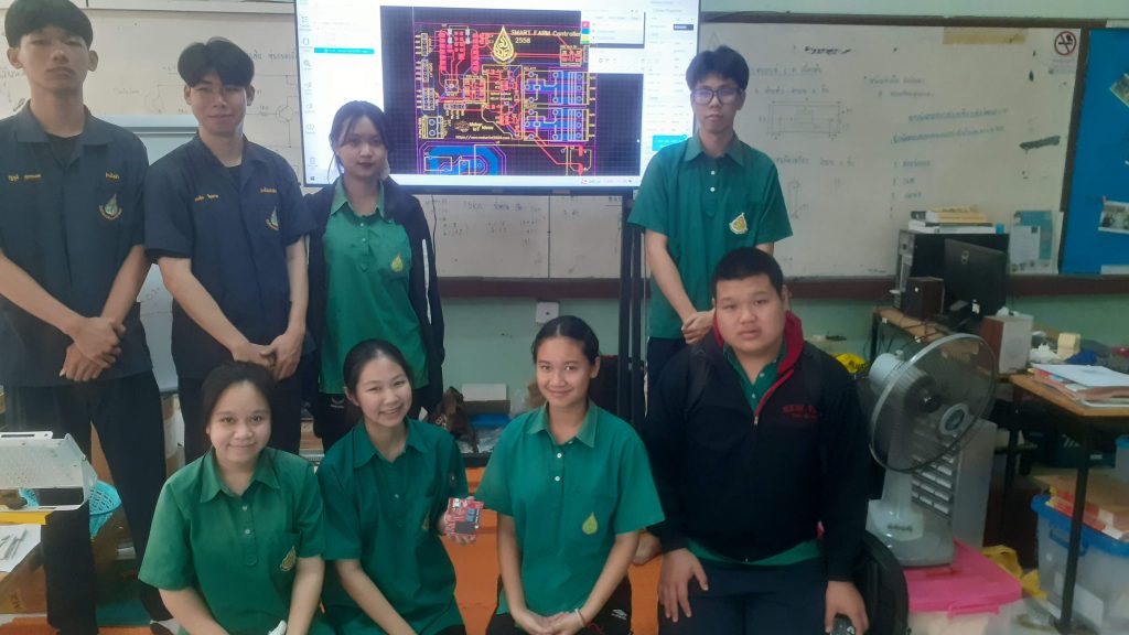
Introduction
Over the last few months, we have been working on several prototypes, and some of our regular visitors may recognise some parts of this PCB. But let us begin by telling you what this is about.
As many of you may know, we have already designed several Can-Bus-related development boards, including one based on the ATTiny1616… So why the repeat then? Well, in some of my previous projects, I hinted at combining a buck converter, boost converter, lipo cell charger and Ideal Diode circuit into one PCB. I did at that time not tell you why.
To make a long story short, this project will eventually be used in my car, to provide more modern cabin lighting, which is quite a bit more than the standard on-or-off and on-when-open-the-door, off-when-close-the-door type of thing…
I own an old Honda City that I use mainly for a run-around to and from the farm, as well as seeing clients… Roads are bad, and this older car (actually quite old – 22 years) is the most cost-effective, in terms of being able to repair by myself, and not be worried about it if it gets a bit abused.
Unfortunately, the technology in the car is dated… a single yellowish cabin light right in the centre of the cabin – and not bright at all. Having to use the car at night, and then frequently scratching around in equipment bags when arriving at a client, becomes a pain with bad light… So I have decided to give it a bit of an upgrade and add CAN-bus-controlled NEO-Pixels to the cabin. For now, let’s say three sets, left, right and centre of the cabin. I also prefer a red light at night over white, especially if I have to drive again soon afterwards – a simple remnant from my days in the military, where it became quite clear how white light can temporarily damage your night vision.
NeoPixels can also be dimmed/brightened and seem relatively inexpensive.
Let us take a closer look at exactly what I want to do…
Powering the module
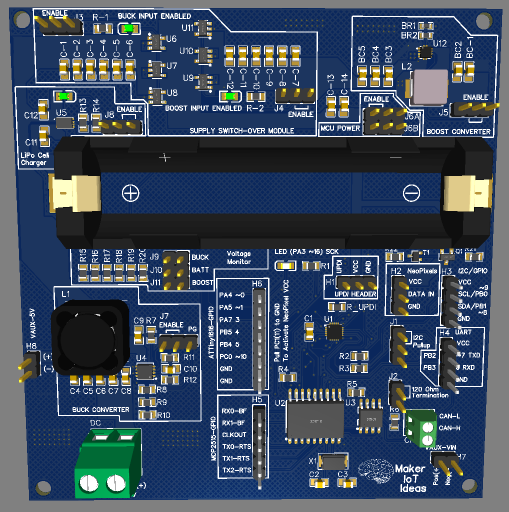
For the sake of clarity, this particular module will be installed front and centre in the cabin, just behind the rearview mirror. It will control two sets of 8 neopixels ( or up to 12 per module ) on two separate PCBs, which will cover the driver and front passenger area of the cabin.
The module will be powered by the vehicle’s 12v battery, as well as from a single 18650 Lipo cell. This means that we would need some clever tricks, in the form of a buck converter to step down the 12v to 5v, a way to monitor and recharge the lipo cell, a boost converter to boost the lipo cell voltage back up to 5v as well as a voltage “OR-ing circuit” to prevent reverse charging the lipo cell etc…
In its current state, the PCB is to be considered a test rig, since I have quite a few unknown variables that need to be thoroughly tested before actually installing this thing into a vehicle.
These are :
1) I would like to know if the ideal diode chip that I used functions well when used in a parallel setup, The reason for that is, that a single chip is capable of just about 1A of current… thus, in my reasoning, placing 3 in parallel would give me the 3A capability that I require – Let’s see if it does…
I could also not get hold of a suitable 3A capable ideal diode chip that was cost-effective, or did not have some strange MOQ or other logistics issues ( Yeah, seems like getting some stuff in SE Asia is difficult unless you are willing to pay unnecessary “special” charges and import duties etc … Element14 ( not sponsored) seems to have a limited selection of ideal diode solutions, but their pricing is good, and there are minimum hassles with shipping etc… I don’t bother with the other two big suppliers, D…. and M…. as they have too much red tape for a hobbyist to navigate to make it cost-effective to shop from them.))
2) Providing that the ideal diode solution does work as expected ( on the PCB) – having tested it on a breadboard seems to be working fine, there is the issue of monitoring the lipo cell, getting it charged, controlling the boost converter to provide power when needed etc…
All of this means that all the separate circuit modules on the PCB can be enabled or disabled by jumpers, and later, if all works as expected, maybe by another controller PCB… Who knows?
Getting back to power the PCB, I have used my standard buck converter circuit, based around the MP9943. This circuit seems to be very reliable, provides enough current, and is cost-effective.
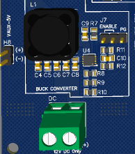
I have also provided an auxiliary voltage output ( 5v) and some telemetry and control capability to the buck converter circuit, in the form of an enable-disable jumper, and the PG signal from the chip, to maybe be interfaced with a microcontroller later.
Charging the Lipo Cell
Once again, I made use of an existing circuit, with which I have had a lot of success in the past. This circuit, based on the MCP73832 from Microchip ( not sponsored) served me quite well in previous projects, and is once again, cost-effective and easy to implement. One negative is that they do seem to be a bit finicky, and not extremely robust – but when they work, they excel at it…
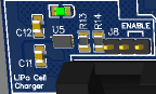
Once again, I decided to provide control logic to enable or disable this part of the circuit completely if needed.
Supply “OR-ing” circuit
This is the most experimental part of this entire circuit board, since, as mentioned above, the MAX40200 is rated at 1A maximum current. It is tiny and cheap, and also readily available… I am hoping that by using them in parallel I can achieve my goal of allowing the full 3A of current to flow from the buck converter, without releasing any “magic smoke” or other issues…
While, at the time of writing, I have not yet received the PCB, I am positive that all may just be fine, it remains to be seen how this will turn out during actual testing of the board.
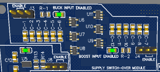
Note that I have used a total of 6 of these, U8 to U11, with 3 per “voltage/current supply” channel. J3 and J4 are used to enable or disable the two supplies, with J3 being the buck converter input, in turn, powered from the vehicle 12v supply, and J4 begin the output from the boost converter, powered by the Lipo cell.
Boost converter circuit and MCU power
The boost converter is based on the MP3423, also from Microchip ( not sponsored). This circuit also performed very well in my initial test projects, with the only issue being it extremely tiny footprint, which really makes it quite difficult to use in a hobby environment, even with hot air and reflow equipment available… It is however also quite cheap, and readily available…
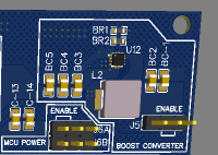
J5 provides enable-disable control to this part of the circuit.
With this relatively complicated power supply circuit, I thought it necessary to be able to completely isolate the ATTiny1616 and other integrated circuits from any power until I am completely sure everything works as planned…
J6A and J6B thus form a complete electrical isolation “breaker” that will prevent any voltage being provided to the microcontroller and other components on the PCB. I have doubled up on these jumpers, to allow for sufficient current flow, since I plan to use quite a few NeoPixels on this PCB… With up to 60mA of current required per pixel, that quickly adds up…
Voltage monitoring
Provision was made to monitor the output voltages of the Lipo Cell, and buck and boost converters by using the analog inputs on the ATTiny1616. These can be selected by setting the jumpers on J9, J10 and J11
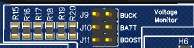
Alternatively, the analog inputs can be used for other applications be leaving the jumpers off, in which case these GPIO’s will be available on H6 as PA4, PA5 and PA7
The ATTiny1616 microcontroller and UPDI programming port
The heart of this PCB is the ATTiny1616 microcontroller, (microchip, not sponsored)
I decided to use the chip once again due to its low cost, as well as the fact that I do not need a very powerful processor for this application. The only issue is that requires UPDI programming. In my case, I have had no issue with that yet, but other readers did mention that they had issues with them…
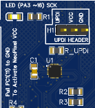
The UPDI header is at H1. This header can also be used to power the processor and other integrated circuits on the PCB independently from the Power supply, like in the case where J6A and J6B are left unconnected. This use case will provide me with more testing opportunities to test the board without possible variables from the power supply circuit(s).
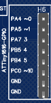
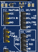
Peripherals like I2C and the UART were broken out onto headers H3 for I2C, H4 for UART. These can also be used as GPIO pins ( remember to disable the I2C pullup in J1)
CAN-Bus Support
CAN-Bus support is provided by the MCP2515 (U2) and TJA1050 (U3) chips.
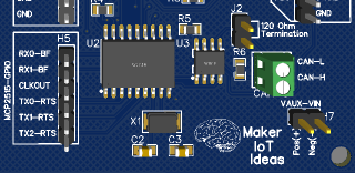
With access to the MCP2515 GPIO pins on H5. J2 is a 120ohm termination resistor, usually enabled at the start and end of the bus to prevent reflections.
CAN-0 is connected to the bus.
An additional 12v input/output header is provided at H7
NeoPixel Header H2
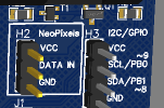
The NeoPixel strips are connected to H2. They are controlled from GPIO PA6 on the ATTiny1616. I have designed around a total of 24 of these at a maximum, with a total current requirement of 1.4A ( 24 x 60mA max per pixel / 1000 = 1.44 A) .
One important fact to know about NeoPixels is that the consume about 1mA per pixel even when in the OFF state. This is due to the internal control chip requiring power to operate. While 1mA bay be a very small amount of current, a lot of them does however quickly add up, and can thus potentially drain a battery completely over time…
To prevent this from happening, I have included a PMOS switch on the VCC pin at H2. This means that no power will be fed to the Neopixel strips unless you specifically pull GPIO PC1 low.
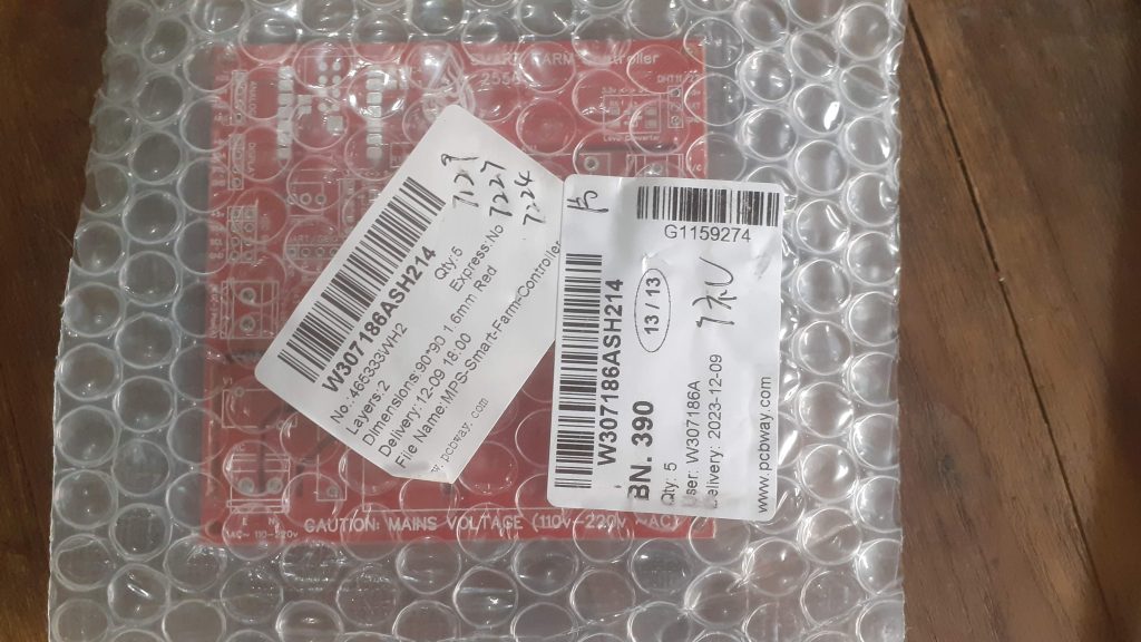
Manufacturing the PCB
I choose PCBWay for my PCB manufacturing. Why? What makes them different from the rest?
PCBWay‘s business goal is to be the most professional PCB manufacturer for prototyping and low-volume production work in the world. With more than a decade in the business, they are committed to meeting the needs of their customers from different industries in terms of quality, delivery, cost-effectiveness and any other demanding requests. As one of the most experienced PCB manufacturers and SMT Assemblers in China, they pride themselves to be our (the Makers) best business partners, as well as good friends in every aspect of our PCB manufacturing needs. They strive to make our R&D work easy and hassle-free.
How do they do that?
PCBWay is NOT a broker. That means that they do all manufacturing and assembly themselves, cutting out all the middlemen, and saving us money.
PCBWay’s online quoting system gives a very detailed and accurate picture of all costs upfront, including components and assembly costs. This saves a lot of time and hassle.
PCBWay gives you one-on-one customer support, that answers you in 5 minutes ( from the Website chat ), or by email within a few hours ( from your personal account manager). Issues are really resolved very quickly, not that there are many anyway, but, as we are all human, it is nice to know that when a gremlin rears its head, you have someone to talk to who will do his/her best to resolve your issue as soon as possible.
Find out more here

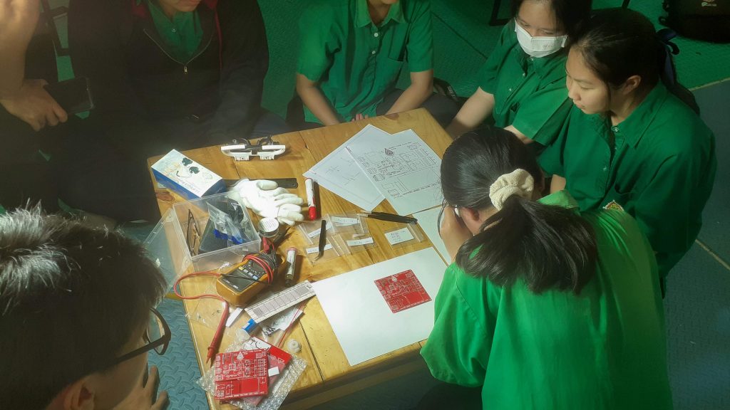
Assembly and Testing
This project has a lot of specific details regarding testing and assembly.
Therefore I have decided to put all of that in a separate post, that you can access
here.