This is a Simple IoT Plant Watering Solution, done as another collaboration with the local High School in my Area. In this project, they took a group of purely academic students ( Language majors ) and told them that they had to design an electronics project that would have use in the real world…
This presented a very tough situation to the students since they had never even imagined that they could do something like this… (Think along the lines of a Senior Design project, like what you would give EE Students during their final year – with all the documentation, pamphlets, and explanations – i.e. lots and lots of paperwork) , and then also add on the requirement that they had to present a practical project as well! And they have only 45 days to do that as well!
I came into this picture late on a Thursday or Friday afternoon, with a group of students milling around outside the Electronics lab. They were unknown to me and seemed quite flustered… I invited them in, and eventually, they started opening up about their problem…
As it turned out, they were completely clueless, and did not know where to start with anything, not even what they wanted to do! Their initial idea went like “something that uses a camera to sort garbage by type and material” – that was never going to happen, not in 45 days, and not with the allocated budget of no more than $USD30.00 they were allowed. Lets not even go to the machine learning stuff, training of the models etc…
So, I took over, and decided that we shall do a simple IoT Plant Watering Solution. It is complex enough for Grade 11 students, and more importantly, I knew that I could teach them enough Arduino coding and basic electronics skills in the time allotted to get the project completed successfully.
What followed was a few very intensive sessions after school to get the paperwork sorted. For some reason, their teacher required ALL paperwork be completed upfront, with the entire design and code prepared before they touched the practical stuff – A funny way to design stuff if you ask me, but that is how we did it…
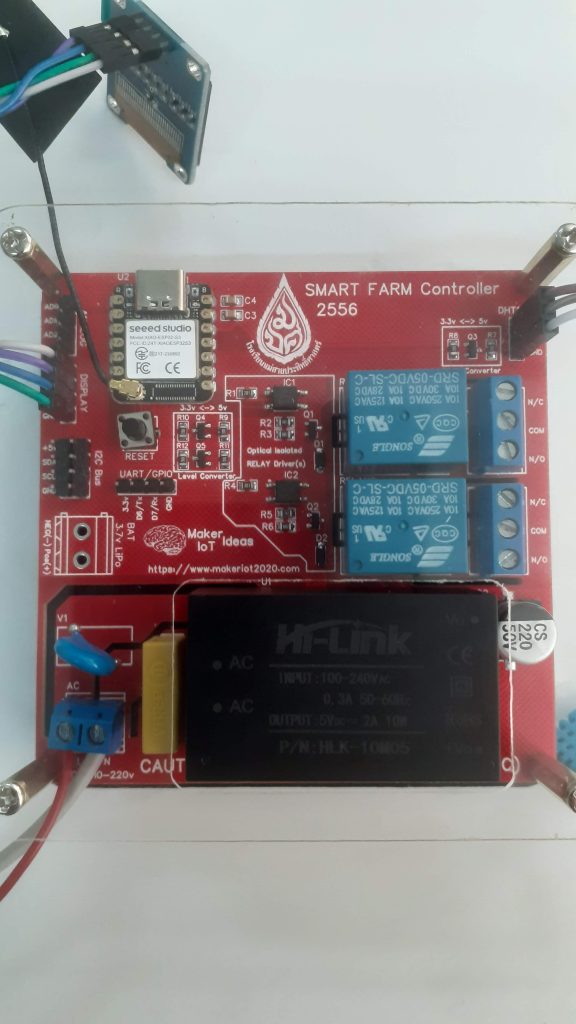
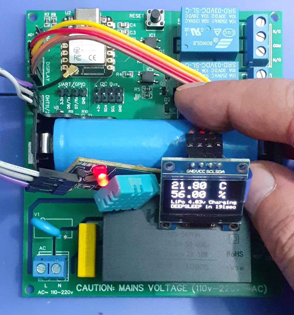
We settled on the ESP8266 12-E NodeMCU v3 development board, A resistive soil sensor, a DHT11 for temperature and humidity data, a small OLED I2C display and a small 5v USB-powered water pump. While they ordered the components, we started with basic coding classes, and this is where the story changes.
These kids blew me away with their level of interest, their attitude to learning, and how quickly they grasped the concepts. In no time at all, they were coding basic sketches, taking readings, learning how the different sensors worked, and pushing the envelope by adding lots more complementary components like MOSFETs and BJT transistors.

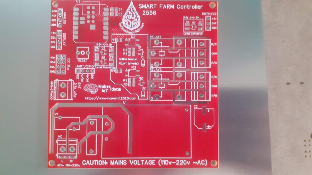
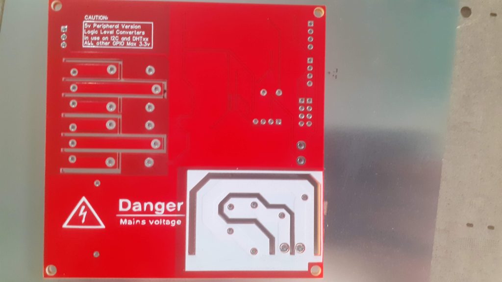
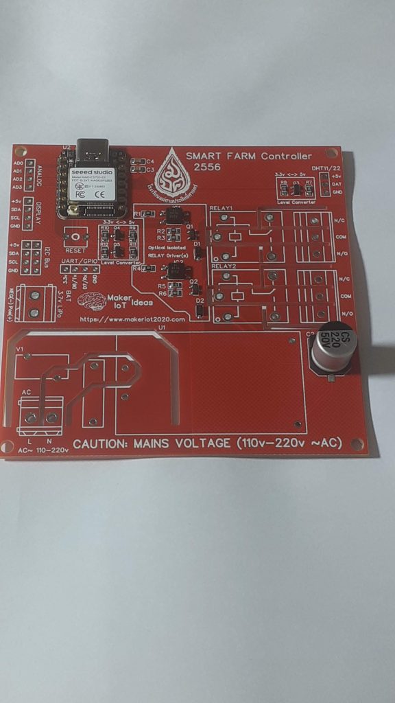
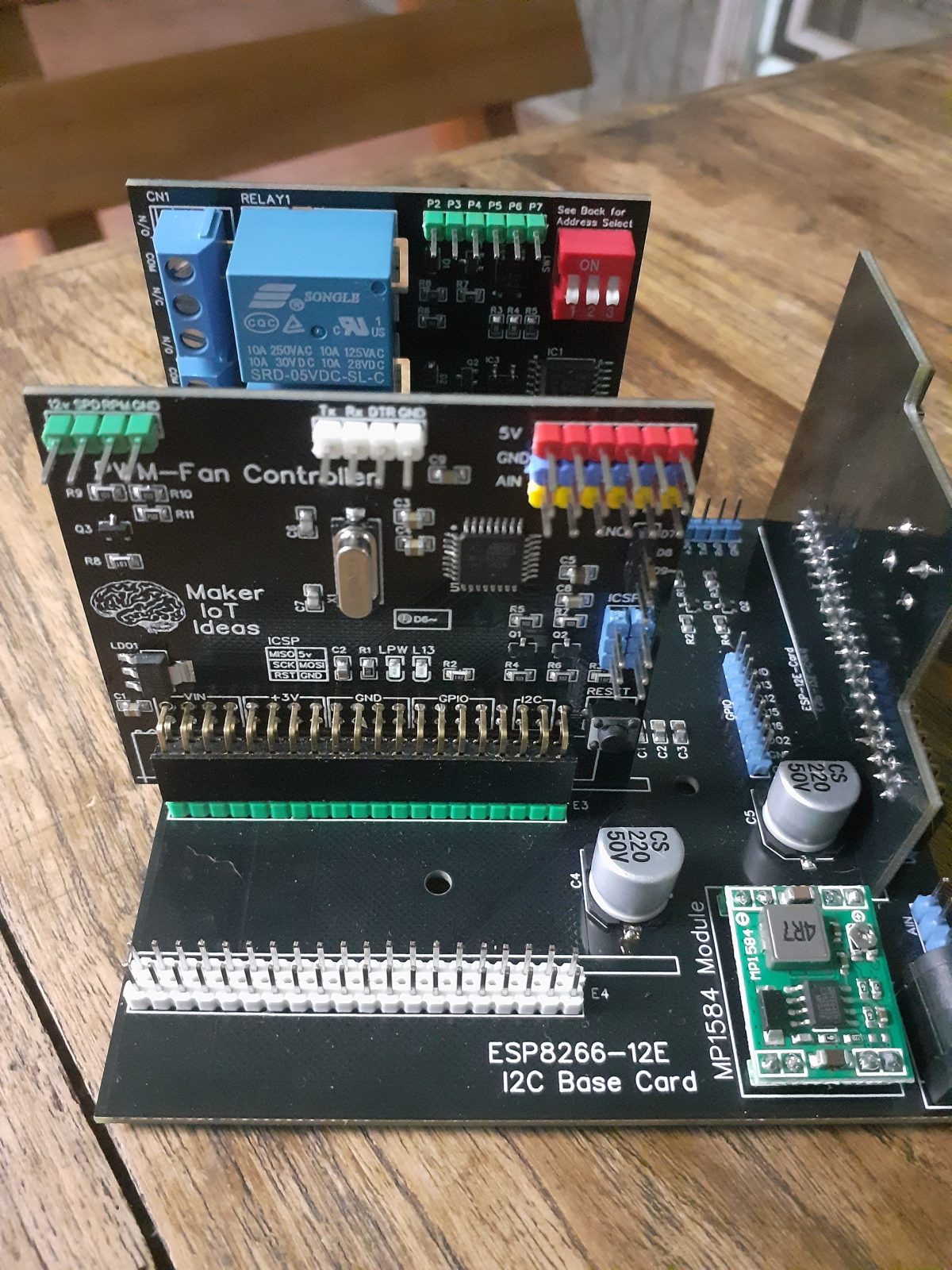
With this level of enthusiasm, I could not help but also become very excited, and thus decided to go a bit further than usual and help them design a neat PCB baseboard for the NodeMCU. That way, we could get rid of all those pesky wire connections, and maybe even produce something that looked good.

This is what we came up with, here shown just after SMD component placing. They ( the students ) did all of that by themselves as well, and it turned out to be a lot of fun for them, with some funny moments for me as well.
The Assembly ( First time ever )
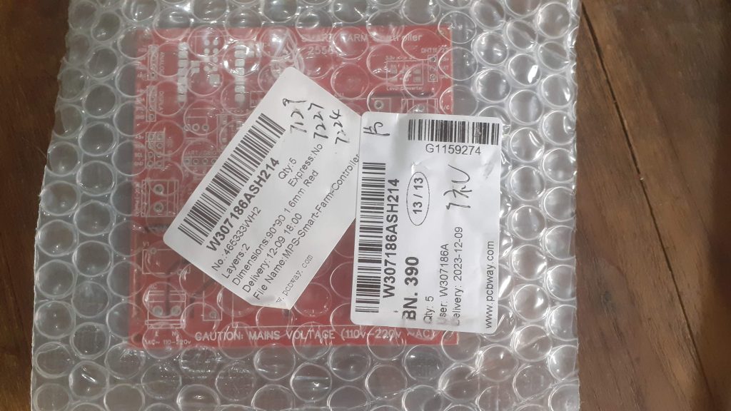
The PCB, together with a stencil, arrived from PCBWay on about the 15th of this month.
I choose PCBWay for my PCB manufacturing. Why? What makes them different from the rest?
PCBWay‘s business goal is to be the most professional PCB manufacturer for prototyping and low-volume production work in the world. With more than a decade in the business, they are committed to meeting the needs of their customers from different industries in terms of quality, delivery, cost-effectiveness and any other demanding requests. As one of the most experienced PCB manufacturers and SMT Assemblers in China, they pride themselves to be our (the Makers) best business partners, as well as good friends in every aspect of our PCB manufacturing needs. They strive to make our R&D work easy and hassle-free.
How do they do that?
PCBWay is NOT a broker. That means that they do all manufacturing and assembly themselves, cutting out all the middlemen, and saving us money.
PCBWay’s online quoting system gives a very detailed and accurate picture of all costs upfront, including components and assembly costs. This saves a lot of time and hassle.
PCBWay gives you one-on-one customer support, that answers you in 5 minutes ( from the Website chat ), or by email within a few hours ( from your personal account manager). Issues are really resolved very quickly, not that there are many anyway, but, as we are all human, it is nice to know that when a gremlin rears its head, you have someone to talk to who will do his/her best to resolve your issue as soon as possible.
Find out more here

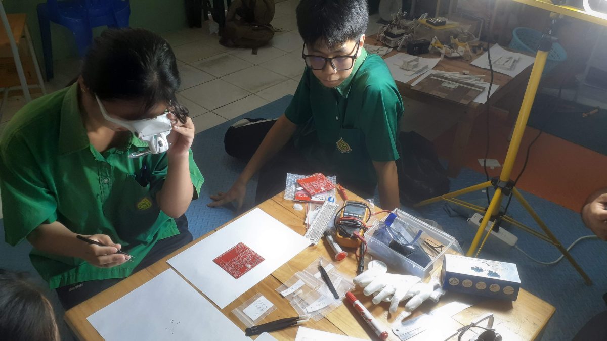
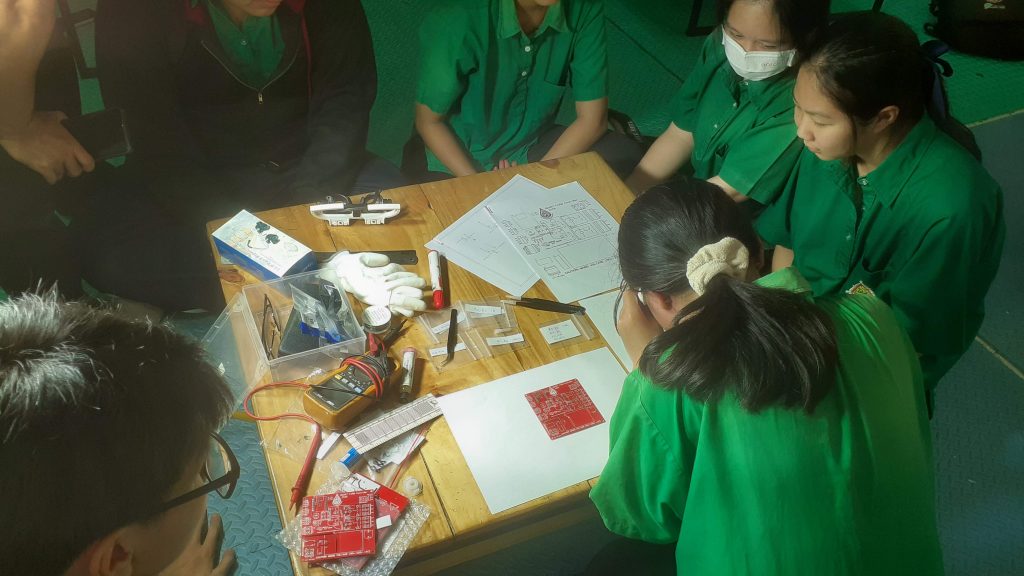
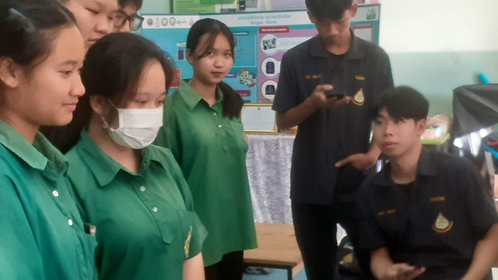
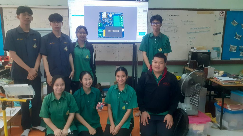
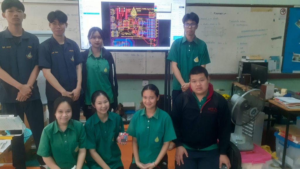
This caused quite a lot of excitement from the students since they asked me to get to school immediately, and offered to stay after school to get the assembly done. So, I packed up all the components required, got in the car, and a few minutes later, we had an assembly line running 🙂


It took them only a few minutes to understand how to read the BOM file, use that information to find the right components and take turns to place a few components at a time onto the PCB. ( I did the solder paste and stencil thing on my own, as that could potentially turn out to be a very messy and wasteful operation if I let them do it )
During this assembly, they were quite amazed at what they were doing, but also quite confused as to how we would ” make the components stick to the PCB later”. They have seen soldering on YouTube, and could not understand how this “grey paste” could “turn hard and shiny” – with some even trying to rush their friends, as the paste would dry up and become sticky…
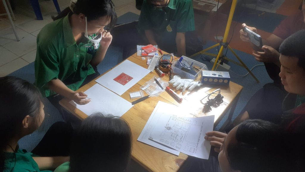
That signalled to me that we should get the hot air ready, and show them properly, as it would stop the speculation, and give them closure on their questions, because no matter how much I tried to explain that the solder paste would be melted later, they could not understand that concept.


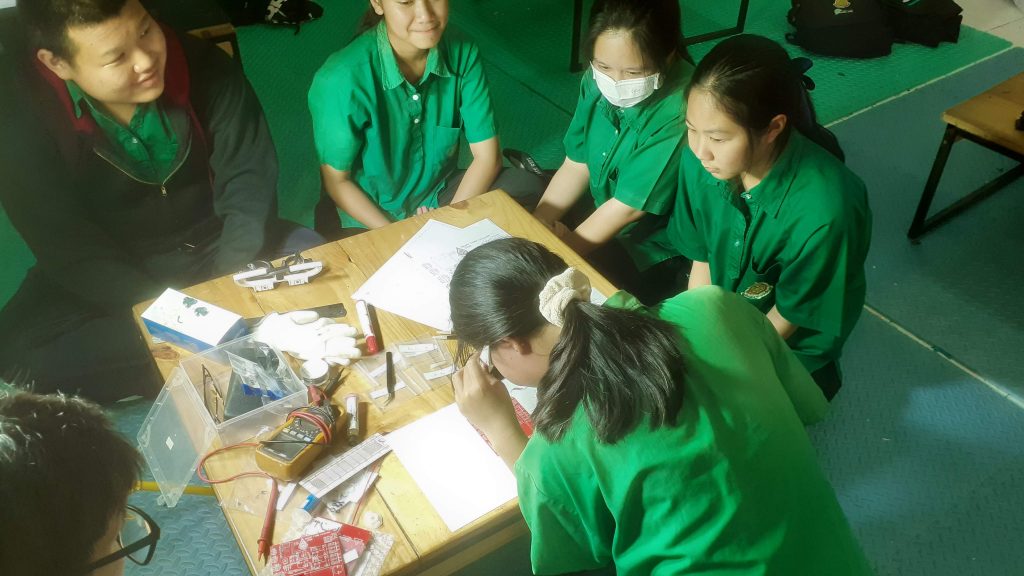
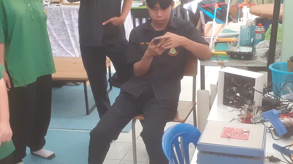
Once I reflowed the first few components using hot air, they all once again took turns with a small group of components on the PCB ( We assembled 2 PCB’s to make sure everybody got a chance to try everything)


Through-hole soldering of the various header pins and other components was next. Once again, I showed them an example and then stepped back while they took over and completed the task. At this time it was about 17:30 already, so I sent them all home, with a promise to return the next day and complete the rest of the build.
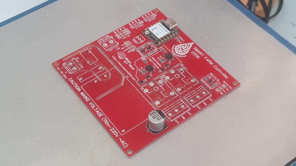
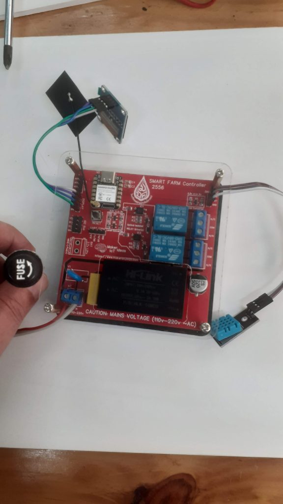
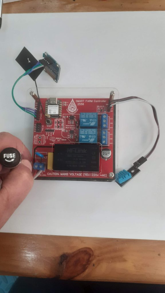
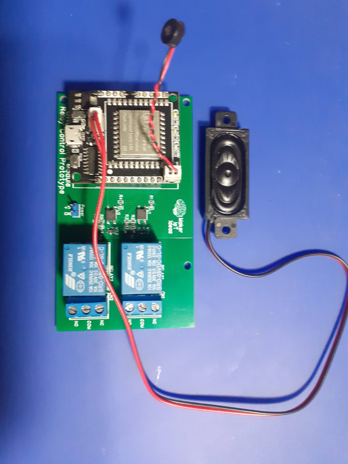
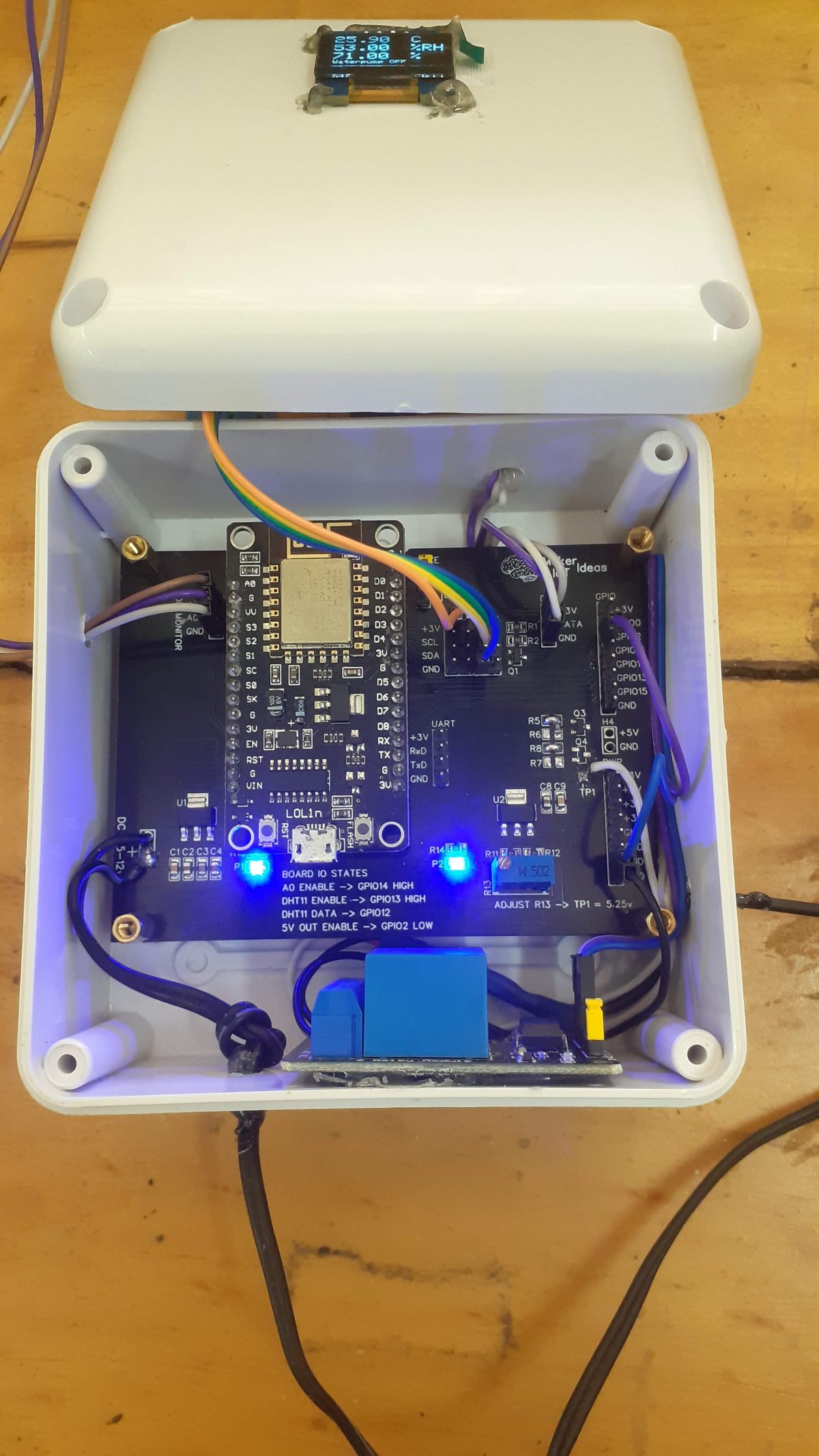
Final Assembly and the Enclosure


We added some copper standoffs to the bottom of the enclosure, drilled some holes and mounted everything with screws and hot glue. The some final testing was performed, and the project was placed outside, next to a potted plant, and put on a sort of soak test, to verify operation for a few days.
A discussion of the circuit
In this circuit, I made use of a very cheap resistive soil moisture probe sensor. It consists of an etched PCB probe and a separate OPAMP on an additional PCB. This assembly then sends an analog voltage back to the Microprocessor for analysis. Very easy to use, and as mentioned, extremely cheap! But this is also a big problem. As seen in many other posts online, people don’t like these probes, as they don’t seem to last very long, and/or become unreliable over time.
I believe that this is due to the fact that they run them continuously, and that, causes the electrodes to erode away over time – because the thing about it, you are basically running an electrolysis cell – sending voltage/current through a probe, that is suspended in a conductive medium ( the water in the soil contains minerals etc – that is why it is conductive, and why we can get a reading from it )
How do I plan to avoid this problem then? The probe is powered through a small N-Channel MOSFET. This allows us to power the probe on when we want a reading, and then power it off again. It will definitely not completely stop the electrodes eroding away over time, but I am sure it will extend the usable lifetime of the probe by quite a bit. On the downside, you need another GPIO pin to control that MOSFET, but that in itself is also a great learning opportunity
Code
#include <SPI.h>
#include <Wire.h>
#include <Adafruit_GFX.h>
#include <Adafruit_SSD1306.h>
#include <Adafruit_Sensor.h>
#include <DHT.h>
#include <DHT_U.h>

#define SCREEN_WIDTH 128 // OLED display width, in pixels
#define SCREEN_HEIGHT 64 // OLED display height, in pixels

#define OLED_RESET     -1 // Reset pin # (or -1 if sharing Arduino reset pin)
#define SCREEN_ADDRESS 0x3C ///< See datasheet for Address; 0x3D for 128x64, 0x3C for 128x32


#define DHTTYPE    DHT11     // DHT 11
#define WaterRelay 2
#define A0Enable 14
#define DHTEnable 13
#define DHTPIN 12
#define WATER_DELAY 10000
#define WATER_LOW 20.00
#define SOIL_DELAY 5000

uint32_t delayMS;
float temperature = 0.00;
float humidity = 0.00;
float soilValue = 0.00;
float soilAverage = 0.00;
unsigned long previousMillis = 0;
unsigned long previousWater = 0;
unsigned long previousSoil = 0;
bool MAY_WATER = 0;
bool RUN_WATER = 0;
bool DELAY_WATER = 0;
sensor_t sensor;
const String WaterOn = "Waterpump ON";
const String WaterOff = "Waterpump OFF";
String WaterMessage = "";

Adafruit_SSD1306 display(SCREEN_WIDTH, SCREEN_HEIGHT, &Wire, OLED_RESET);
DHT_Unified dht(DHTPIN, DHTTYPE);


void setup() {

  pinMode(WaterRelay,OUTPUT);
  pinMode(A0Enable,OUTPUT);
  pinMode(DHTEnable,OUTPUT);
  digitalWrite(WaterRelay,HIGH);
  //Serial.begin(115200);
  if(!display.begin(SSD1306_SWITCHCAPVCC, SCREEN_ADDRESS)) {
    //Serial.println(F("SSD1306 allocation failed"));
    for(;;); // Don't proceed, loop forever
  }
  display.ssd1306_command(SSD1306_DISPLAYON);
  display.clearDisplay();
  display.display();
  delay(20);
  display.setTextSize(1);
  display.setTextColor(SSD1306_WHITE);
  display.setCursor(10,10);
  display.print("Booting...");
  display.display();
  delay(2000);

  dht.begin();

  show_DHT_Params();

}

void loop() {


  //Soil Monitor Loop
  unsigned long SoilMillis = millis();
  if ( SoilMillis - previousSoil >= SOIL_DELAY) {
    previousSoil = SoilMillis;
    take_soil_reading();
  }
  //End Soil Monitor Loop

  //Water Loop
  unsigned long WaterMillis = millis();
  if (WaterMillis - previousWater >= WATER_DELAY) {
    previousWater = WaterMillis;
    if ((digitalRead(WaterRelay) == LOW) && (RUN_WATER == 1) && ( DELAY_WATER == 0)) {
      digitalWrite(WaterRelay,HIGH);
      DELAY_WATER = 1;
    } else if (DELAY_WATER == 1) {
      DELAY_WATER = 0;
      if (RUN_WATER == 1) RUN_WATER = 0;
    }
  }
  // End Water Loop
  // Main One Second Delay Loop
  unsigned long currentMillis = millis();
  if (currentMillis - previousMillis >= delayMS) {
    previousMillis = currentMillis;
    get_DHT_Readings();
    show_Soil_Data();
    display.display();
  }
  // End Main 1 Second Loop
  if ((soilAverage < WATER_LOW) && (RUN_WATER == 0)) {
    RUN_WATER = 1;
    MAY_WATER = 1;
  } else if (soilAverage >= WATER_LOW) {
    RUN_WATER = 0;
    MAY_WATER = 0;
  }

  if ((digitalRead(WaterRelay) == HIGH) && (RUN_WATER == 1) && DELAY_WATER == 0) {
      digitalWrite(WaterRelay,LOW);
      WaterMessage = WaterOn;
      take_soil_reading();
  }
  if ((DELAY_WATER == 1) && (MAY_WATER == 1)) {
      digitalWrite(WaterRelay,HIGH);
      WaterMessage = WaterOff;
  }

}

void take_soil_reading() {
  digitalWrite(A0Enable,HIGH);
  delay(50);

  float tempSoil = 0.00;
  for (int i = 0; i <10 ; i++) {
    soilValue = (1024.00 - analogRead(A0));
    tempSoil = tempSoil + soilValue;
    delay(2);
  }
  soilAverage = map(tempSoil/10,0.00,1023.00,0.00,100.00);
  delay(30);
  digitalWrite(A0Enable,LOW);
}

void show_DHT_Params() {
  digitalWrite(DHTEnable,HIGH);

  dht.temperature().getSensor(&sensor);
  display.clearDisplay();
  display.display();
  display.setTextSize(1);
  display.setTextColor(SSD1306_WHITE);
  display.setCursor(10,1);
  display.print("Temperature Sensor");
  display.setCursor(10,10);
  display.print(F("Type: "));
  display.print(sensor.version);
  display.setCursor(10,20);
  display.print(F("Min: "));
  display.print(sensor.min_value);
  display.print(F(" Deg C"));
  display.setCursor(10,30);
  display.print(F("Max: "));
  display.print(sensor.max_value);
  display.print(F(" Deg C"));
  display.setCursor(10,40);
  display.print(F("Resolution: +/- "));
  display.setCursor(10,50);
  display.print(sensor.resolution);
  display.print(F(" Deg C"));
  display.display();
  delay(4000);
  dht.humidity().getSensor(&sensor);
  display.clearDisplay();
  display.display();
  display.setTextSize(1);
  display.setTextColor(SSD1306_WHITE);
  display.setCursor(10,1);
  display.print("Humidity Sensor");
  display.setCursor(10,10);
  display.print(F("Type: "));
  display.print(sensor.version);
  display.setCursor(10,20);
  display.print(F("Min: "));
  display.print(sensor.min_value);
  display.print(F(" % RH"));
  display.setCursor(10,30);
  display.print(F("Max: "));
  display.print(sensor.max_value);
  display.print(F(" % RH"));
  display.setCursor(10,40);
  display.print(F("Resolution: +/- "));
   display.setCursor(10,50);
  display.print(sensor.resolution);
  display.print(F(" % RH"));
  display.display();
  delay(4000);

  delayMS = sensor.min_delay / 1000;
}

void get_DHT_Readings() {

    display.clearDisplay();
    display.setTextSize(2);
    display.setTextColor(SSD1306_WHITE);
    sensors_event_t event;
    dht.temperature().getEvent(&event);
    if (isnan(event.temperature)) {
      #ifdef DEBUG-SERIAL
      Serial.println(F("Error reading temperature!"));
      #endif
    }
    else {
      display.setCursor(10,1);

      display.setCursor(10,1);
      display.print(event.temperature);
      display.setCursor(80,1);
      display.println(F(" C"));
      temperature = event.temperature;
    }
    // Get humidity event and print its value.
    dht.humidity().getEvent(&event);
    if (isnan(event.relative_humidity)) {
     display.clearDisplay();
    display.setTextSize(2);
    display.setTextColor(SSD1306_WHITE);
    sensors_event_t event;
    dht.temperature().getEvent(&event);
    if (isnan(event.temperature)) {
      #ifdef DEBUG-SERIAL
      Serial.println(F("Error reading temperature!"));
      #endif
    }
    else {

      display.setCursor(10,1);
      display.print(event.temperature);
      display.setCursor(80,1);
      display.println(F(" C"));
      temperature = event.temperature;
    }
    // Get humidity event and print its value.
    dht.humidity().getEvent(&event);
    if (isnan(event.relative_humidity)) {
      #ifdef DEBUG-SERIAL
      Serial.println(F("Error reading humidity!"));
      #endif
    }
    else {
      display.setCursor(10,20);
      display.print(event.relative_humidity);
      display.setCursor(80,20);
      display.println(F(" %"));
      humidity = event.relative_humidity;
    }
    }
    else {
      display.setCursor(10,20);
      display.print(event.relative_humidity);
      display.setCursor(80,20);
      display.println(F(" %RH"));
      humidity = event.relative_humidity;
    }

}

void show_Soil_Data() {
  display.setTextSize(2);
  display.setTextColor(SSD1306_WHITE);
  display.setCursor(10,39);
  display.print(soilAverage);
  display.setCursor(80,39);
  display.println(F(" %"));
  display.setTextSize(1);
  display.setCursor(10,56);
  display.println(WaterMessage);
}
Conclusion
This project was extremely interesting. It was something very basic, but it gave me a very unique opportunity to teach a group of kids something they never knew before. It also initiated a spark in many of them, who are now interested in getting involved in electronics as a hobby. The possibilities of this project, if it is improved a bit more, could also be great. For example, we did not even consider adding IoT connectivity to this yet, we all decided that it was not needed, and an unnecessary complication of an already complex issue ( to the students that is). I shall keep monitoring the operation of the device over the next few weeks, and hopefully get some answers myself as to how long that soil probe will last… As a control, we have another one that was left powered on in the same container. That one are not being used to take readings, but will definitely provide us with a good comparison against the probe that is only on then used…