USB Ports are quite handy to power all our day-to-day electronic devices, but most charging devices are limited to a single port. While it is possible to get a commercial multi-port USB-Charger ( I have quite a few myself), they are usually limited in charging current or very cheaply made.
I decided to do my own, at this time limited to supplying power only, but with a few added features to make it my own.
Features
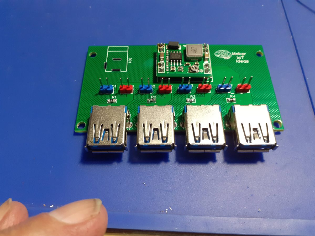
- Individual switching of ports
- Individual power LED indicator on each port, that can be left disconnected for total dark operation ( I don’t like charging lights in the bedroom )
- Switchmode Power Supply unit, up to 2A output
- Wide input supply options, not limited to 5v
- Wide power tracks to ensure decent current transfer, and reduce heat generation on the PCB
Why did I choose to build my own?
We use USB ports on almost all our electronics devices, and most of the charging units that comes with these are quite badly designed. They are underpowered, have only one port, and have annoying lights that are quite bright at night.
I wanted a single unit that can accept up to 4 devices, control each port individually, as well as be relatively small and compact for travel use.
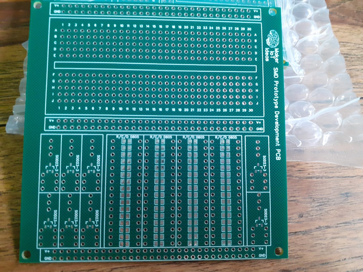
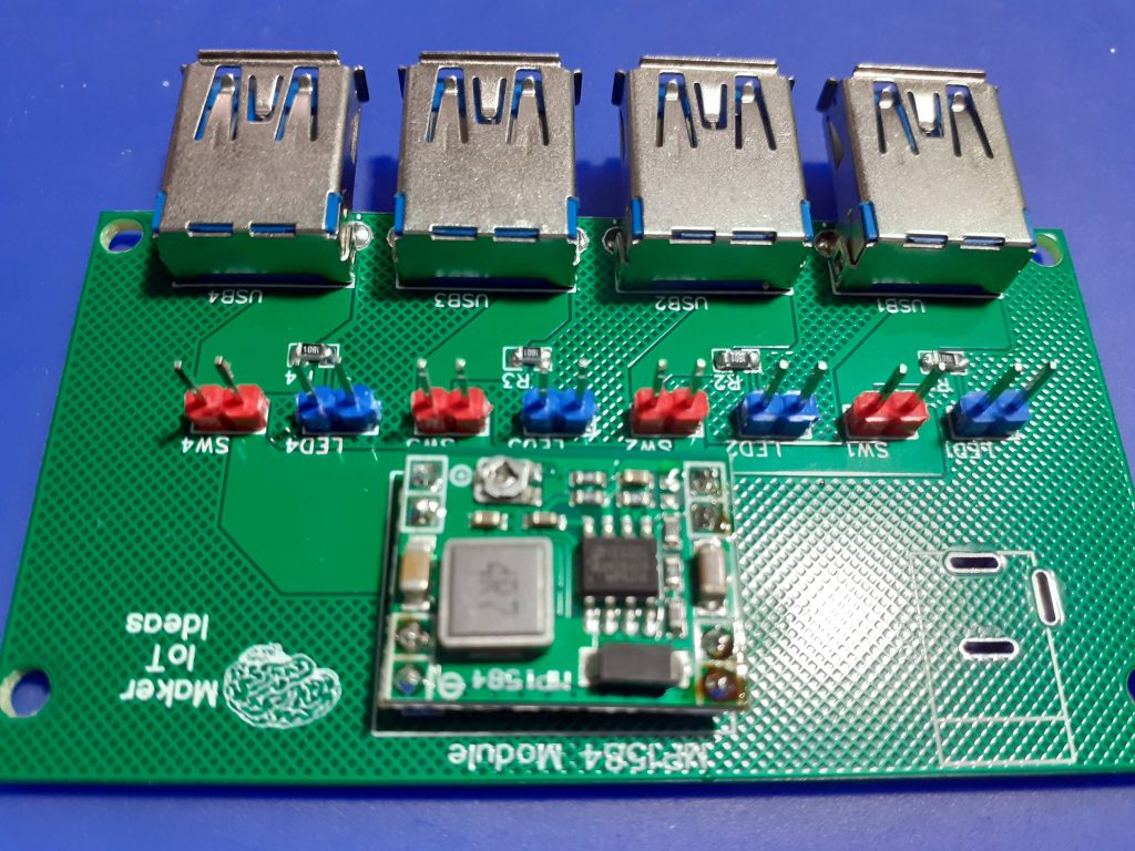
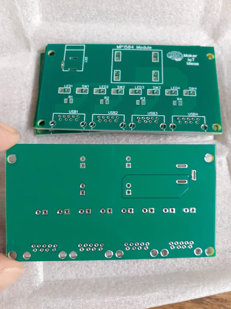
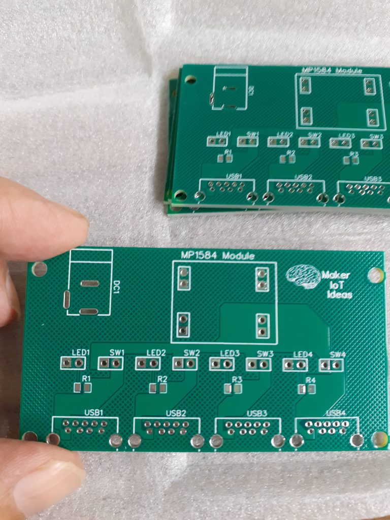
The PCB
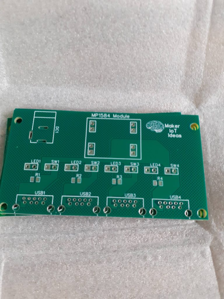
The PCB is a double layer, with wide power tracks on opposite sides of the board. The component count is quite low, with only USB3 Type Female connectors(4), a single MP1584 Buck converter module, 4x current limiting resistors for the LED indicators, as well as male header pins for the switches and LED indicators.
The biggest challenge was to get the port spacing correct so that it will be easy to use all of them at the same time. CNC cutting the enclosure should also not be too difficult as well, once I get around to designing that in CAD/CAM
The Schematic
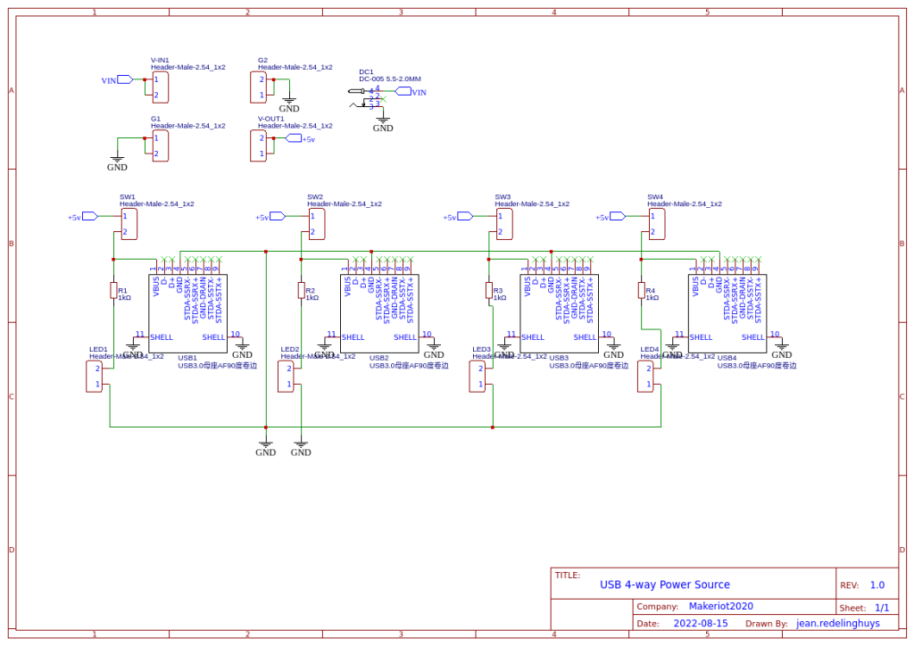
I have chosen to keep it simple on this revision, and only supply power via the ports. I plan to maybe do a full data-capable USB 3.0/ USB3.1 Hub later.
Manufacturing
Over the past eight years, PCBWay has continuously upgraded their MANUFACTURING plants and equipment to meet higher quality requirements, and now THEY also provide OEM services to build your products from ideas to mass production and access to the market.
The PCB for this project has been manufactured at PCBWay.
Please consider supporting them if you would like your own copy of this PCB, or if you have any PCB of your own that you need to have manufactured.

If you would like to have PCBWAY manufacture one of your own, designs, or even this particular PCB, you need to do the following…
1) Click on this link
2) Create an account if you have not already got one of your own.
If you use the link above, you will also instantly receive a $5 USD coupon, which you can use on your first or any other order later. (Disclaimer: I will earn a small referral fee from PCBWay. This referral fee will not affect the cost of your order, nor will you pay any part thereof.)
3) Once you have gone to their website, and created an account, or login with your existing account,
4) Click on PCB Instant Quote

5) If you do not have any very special requirements for your PCB, click on Quick-order PCB

6) Click on Add Gerber File, and select your Gerber file(s) from your computer. Most of your PCB details will now be automatically selected, leaving you to only select the solder mask and silk-screen colour, as well as to remove the order number or not. You can of course fine-tune everything exactly as you want as well.
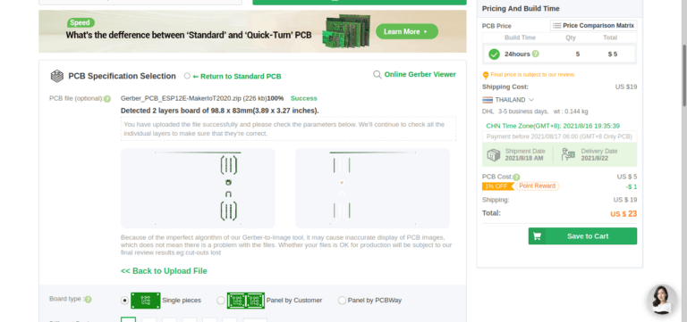

7) You can also select whether you want an SMD stencil, or have the board assembled after manufacturing. Please note that the assembly service, as well as the cost of your components, ARE NOT included in the initial quoted price. ( The quote will update depending on what options you select ).
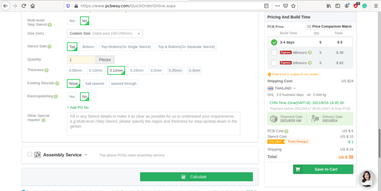
8) When you are happy with the options that you have selected, you can click on the Save to Cart Button. From here on, you can go to the top of the screen, click on Cart, make any payment(s) or use any coupons that you have in your account.
Then just sit back and wait for your new PCB to be delivered to your door via the shipping company that you have selected during checkout.