As part of my current project to add NeoPixels to the cabin of my car – as an upgrade to an old run-around vehicle, I had various ideas. One of these was to have pixels in multiple locations in the cabin, for example, next to the rear doors on each side, as well as in the current location of the current, sad old yellow light, in the centre of the cabin. These pixels should be controllable from a central location, on the front dash of the vehicle, or above the rearview mirror, as well as have local control.

CAN-BUS seemed the logical way to have central control over all of these, and as far as local control goes, I don’t necessarily want to go messing with the 20-odd-year-old wiring of the car, it is problematic already, and my interference could just potentially make things worse. ( living in super humid SE Asia takes its toll on the wiring, and local auto-electricians make more than a mess than fix anything – while still maintaining their “standard” of high-quality pricing for an ultra-low quality job – thus scrap that right from the beginning)
I have thus decided on a three-pushbutton approach, White light, on and off, Red light on and off, and increase/decrease intensity ( I really want the red cabin lights, as it helps to preserve night vision as opposed to white)
This project is not thus a less complicated version of this,
which is the main controller PCB, minus a few components, for example:
No Buck converter – just a single LDO regulator
No Supply OR-Ing logic, as there will be only a single supply
No Battery charger, and for that matter Boost converter.
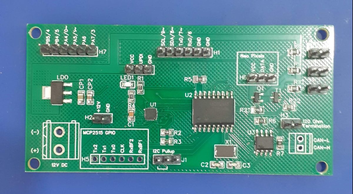
The board still uses the ATTiny1616 microcontroller ( I had a few in stock, and since I don’t need a lot of power for this, they are ideal).
CAN-BUS support is provided with an MCP2515 and supporting circuitry.
All GPIO’s on the ATTiny1616 and MCP2515 are broken out for easy access, so it is possible to really hack this board into anything needed within reason.
The NeoPixels VCC line is also controlled via a P-MOS switch, to keep them totally switched off until actually needed, thus saving a few milliamps of battery power.

The Schematic
I have decided to include the schematics as downloadable .png files. just click on the images for a high-resolution picture that you can download to your device.


Manufacturing the PCB
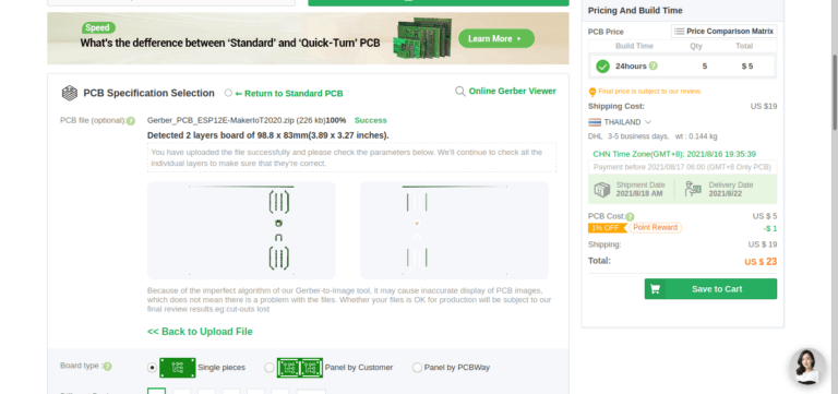
I choose PCBWay for my PCB manufacturing. Why? What makes them different from the rest?
PCBWay‘s business goal is to be the most professional PCB manufacturer for prototyping and low-volume production work in the world. With more than a decade in the business, they are committed to meeting the needs of their customers from different industries in terms of quality, delivery, cost-effectiveness and any other demanding requests. As one of the most experienced PCB manufacturers and SMT Assemblers in China, they pride themselves to be our (the Makers) best business partners, as well as good friends in every aspect of our PCB manufacturing needs. They strive to make our R&D work easy and hassle-free.
How do they do that?
PCBWay is NOT a broker. That means that they do all manufacturing and assembly themselves, cutting out all the middlemen, and saving us money.
PCBWay’s online quoting system gives a very detailed and accurate picture of all costs upfront, including components and assembly costs. This saves a lot of time and hassle.
PCBWay gives you one-on-one customer support, that answers you in 5 minutes ( from the Website chat ), or by email within a few hours ( from your personal account manager). Issues are really resolved very quickly, not that there are many anyway, but, as we are all human, it is nice to know that when a gremlin rears its head, you have someone to talk to who will do his/her best to resolve your issue as soon as possible.
Find out more here

Assembly and Testing
Assembly is easy, if you use a stencil. The ATTiny 1616 QFN package will give you a hard time without a precise way to apply just the right amount of solder paste to the pads.

Testing
As far as testing goes, I am busy with the final firmware of this board.
I will however go over a few things:
The UPDI programming header functions as expected, using my own programmer, and the Arduino IDE.
A standard blink sketch works as expected ( LED is on PIN_PA3)
This is also the SPI SCK pin.
The CAN BUS hardware functions as expected ( Using the MCPCan library)
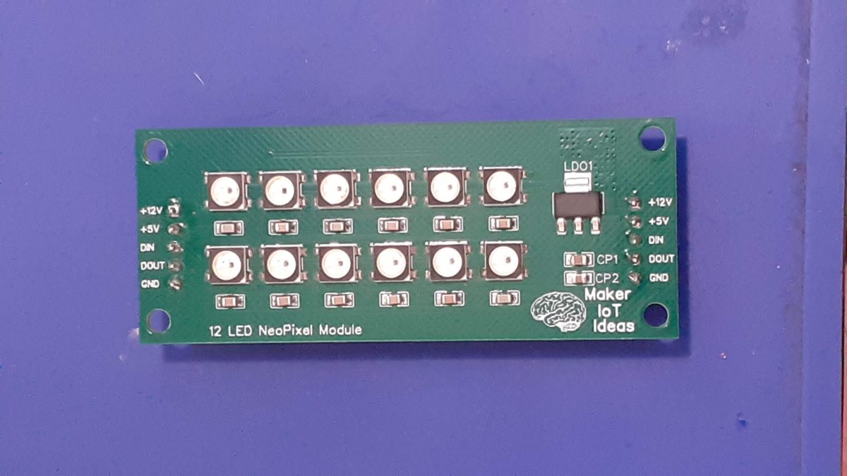
A small NEOPixel strip ( 8 pixels ) connected to the module and controlled with the Adafruit NeoPixel library functions as expected – Note here that you HAVE to enable power to the pixels by pulling PC0 ( PIN_PC0) HIGH to enable the P-MOS Switch. The Pixels themselves are connected to PIN_PA6.
The 3 pushbutton switches function as expected, and are connected on PIN_PC1 to PIN_PC3, each with an external 10k pullup resistor.
I shall update further progress on the project as it becomes available. I am currently working on firmware, as well as designing a suitable enclosure to be CNC cut from acrylic.
Powering the modules in the actual vehicle shall also require some clever thinking, as I do not want them draining the car battery – I am thinking about either using the existing door-open switches or maybe an interface from the ignition to only power them when the ignition is switched on.