

ATTiny1616 QFN with Can bus support on a breadboard
A short while ago, I started looking at alternatives to the ATMEGA328P ( the chip used in the standard Arduino Uno). That experiment turned out quite well,
with two of the three chips turning out to be useful, the ATTiny1616 and the Atmega 4808 – The ATTiny 202, while working great, has quite a few severe limitations, due to the size of its memory, as well as library support, limiting its actual useful use quite a bit for my purposes.
In this post, which is part of a two-part series, I will look at adding dedicated CAN Bus support to the 1616 and 8408. I am planning to add some gadgets to my car, and would like to have it controlled by a CAN bus interface, and just maybe, interfacing with the CAN bus on the car as well – at least in the future…
This experiment will thus consist of two prototypes with onboard CAN hardware, to be initially used on the bench while building and testing my gadgets – more on them later, if and when they work out the way that I imagine.
What is on the PCB
The ATTiny1616 microcontroller, in a QFN package, has been married to a MCP2515 and a TJA1050. These chips, while old, are still easy to get hold of,
and I have quite a few of them lying around from previous projects. It did thus seem to be a good starting point. The fact that their libraries also works perfectly with the ATTiny1616 and Atmega4808 also went a long way towards selecting them for the project.
The PCB is similar to the ATTiny1616 QFN breakout that I have designed before but with the addition of the CAN-related components.

ATTiny1616 QFN development board with CAN bus, after reflow soldering
Schematic and PCB Design
The schematic is a variation on the earlier breakout PBC, with the addition of the CAN-related components.


The PCB design has also not changed a lot, I have just added the CAN components to the right hand side of the PCB, and adjusted the routing.


3D render of the PCB, with the header pins in non-breadboard configuration – with the CAN bus connector not fitted.
Manufacturing
I choose PCBWay for my PCB manufacturing. Why? What makes them different from the rest?
PCBWay‘s business goal is to be the most professional PCB manufacturer for prototyping and low-volume production work in the world. With more than a decade in the business, they are committed to meeting the needs of their customers from different industries in terms of quality, delivery, cost-effectiveness and any other demanding requests. As one of the most experienced PCB manufacturers and SMT Assemblers in China, they pride themselves to be our (the Makers) best business partners, as well as good friends in every aspect of our PCB manufacturing needs. They strive to make our R&D work easy and hassle-free.
How do they do that?
PCBWay is NOT a broker. That means that they do all manufacturing and assembly themselves, cutting out all the middlemen, and saving us money.
PCBWay’s online quoting system gives a very detailed and accurate picture of all costs upfront, including components and assembly costs. This saves a lot of time and hassle.
PCBWay gives you one-on-one customer support, that answers you in 5 minutes ( from the Website chat ), or by email within a few hours ( from your personal account manager). Issues are really resolved very quickly, not that there are many anyway, but, as we are all human, it is nice to know that when a gremlin rears its head, you have someone to talk to that will do his/her best to resolve your issue as soon as possible.
Find out more here

Assembly
I usually can not wait to receive my creations back from the factory – I mean, how can somebody not get excited about receiving their own PCBs back from the factory, especially if you know they will be of the high quality that I have come to trust with all of my PCBWay orders?
This is especially true of the smaller PCBs, as well as those with smaller-sized QFN components, with this board definitely not being an exception.


This PCB once again requires the use of a stencil, to accurately apply just the right amount of solder paste to the pads, especially the small QFN package pads of the ATTiny 1616…

Stencils, at least from my point of view, can be a controversial subject, with some hobbyists arguing that they are not worth the additional expense… I do however believe that they actually save you a lot, in time that you don’t waste on reworking a PCB due to solder bridges, in the correct amount of solder paste that is applied, in the correct thickness, and also time not wasted on the cleanup of the mess that can result from manually applying solder paste.

The PCB is now reflow soldered with a hot plate, and allowed to slowly cool down afterwards, to reduce thermal shock damage to the joints, that may result from a too-quick cooldown cycle. While I do not own a dedicated reflow oven, the hotplate that I use, seems to match the reflow profile ramp-up of my solder paste, and most of the components perfectly. After achieving a complete solder melt, at about 223 degrees C, I usually switch of the hot plate, and carefully move the PCB towards the edge of the unit, that area is usually a bit cooler than the centre. leaving it there for about 5 to 8 minutes, allow the solder to slowly solidify, after which I remove it and place it on a silicone mat to cool completely.

Through-hole component soldering, and testing
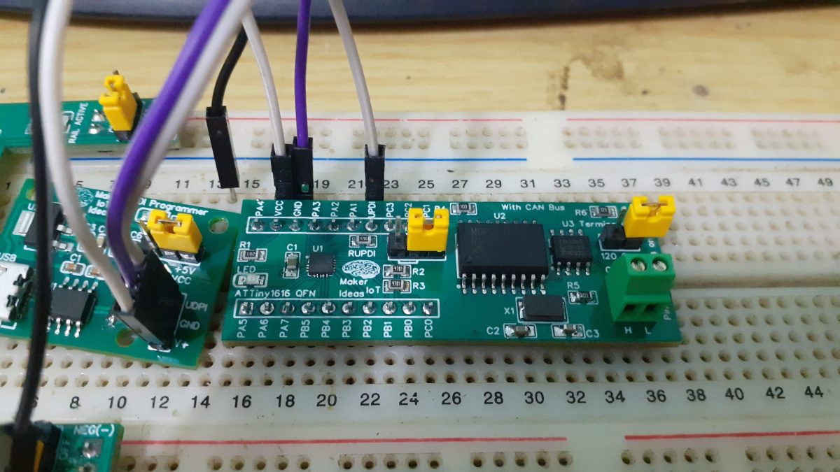
The next step is soldering all the through-hole components, usually header pins and connectors into their respective places. The board is then placed onto a solderless breadboard, and various test sketches are uploaded via a homemade UPDI programmer.
These include the infamous blink sketch, to make sure the chip is alive and survived the reflow soldering. That is followed by a CAN loopback test, and then the actual CAN firmware… I make use of the excellent MCP Can library from Garry J Fowler, as well as the megaTinyCore Arduino core, from Spence Konde.
My thanks to both of these gentlemen, for their excellent and easy-to-use software. A special shoutout to Garry J Fowler, since his MCP Can library correctly releases the CE pin of the device when not in use, thus not locking up the spi bus. [ This is something that many other libraries do not bother to care about ] …
Conclusion
This was once again a fun project to design and assemble. The real testing and development can now start at full speed, as this is just meant to be a tool, with a further revision later down the line. It does of course help a whole lot that I can completely trust my PCB manufacturer, PCBWay, to deliver my PCBs to me EXACTLY as I designed them, and at extremely high quality and precision! Thank you for that!