
(Design for Manufacturability) Gerber Software Analyser
Free to Use for all PCBpartner.com Users

PCBPartner.com recently decided to release their own DFM software, which I believe they developed in-house and use themselves every day, to their customers, in order to enable their customers to design better PCBs and increase the overall quality and service satisfaction.
In this article, I will give the software a quick look and feel, and show you some of its features, while at the same time admitting upfront, that it is quite complex, and that I am also not quite well acquainted with it myself, having only a few days to play with it up to now.
What is DFM?

DFM (Design for manufacturability) analysis of incoming Gerber files is a standard and important process in any PCB factory. iPCB-DFM’s purpose is to perform this process automatically to find potential production issues with your PCB design, saving time and effort for you the PCB designer, and the PCB manufacturing engineers who are going to produce your PCB. Based on 25 years of PCB manufacturing experience, we have a massive collection of PCB DFM rules built into this software, allowing it to analyze up to 24 kinds of specifications.
It also has powerful features such as quick panalization, PCB simulation and direct Gerber editing, and can even help you count how many SMD pads are in your design!
Why do you need iPCB-DFM?
If you’re an electronic engineer, you don’t want to send your PCB Gerber files for manufacturing without checking that your design and file formats match your factory’s production capability; If you are a purchasing manager without much knowledge of PCB manufacturing processes, this tool can help you better understand the specifics of the PCBs you are ordering, making it much easier to communicate with your PCB suppliers.
What Features does this DFM have?
Gerber file view supports Gerber274x, Excellon, ODB++ and IPC-2581 formats
-Measuring
-Layer management
-Auto recognize layers (silkscreen, solder mask, copper, solder paste, inner layers)

-PCB simulation:
generate a simulated preview of your PCB, updated in real-time by different colour settings and surface finishes, and supporting high-resolution PNG output format.
DFM Functions
1 Layer
2 Dimension
3 Minimum trace space
4 Minimum trace width
5 Hole diameter
6 Drill slot
7 Through-hole annular ring
8 Hole distance
9 Hole to trace
10 Copper to edge
11 Special holes
12 SMD size
13 Via in pads
14 Test Point
15 Component solder pads number
16 Via density
17 Surface finish area (%)
18 Routing length of travel
19 Grid wiring
20 Solder mask
21 Fiducial Point
22 SMD pad size
23 SMD pad space
24 BGAs
Gerber Edit
1 Add elements
2 Delete elements
3 Move elements
4 Copy elements
5 Adjust circuit angle
6 Rotate elements
7 Edit trace
8 Mirror
9 Positive and negative switch
10 Break trace
11 Shape edit
12 Single, rectangular marquee, polygon selection
Panelization
Quick panelization
– set a panelization style, tooling bar width and board space,
one click to generate a panalized board in seconds in Gerber format.
Advanced panelization – allows you to adjust tooling hole, v-cut, fiducial mark, solder mask for fiducial mark, drill holes on tooling bar, etc.
What does it need to run?
For the foreseeable time forward, the software only runs on Microsoft Windows. It apparently supports from Windows XP right up to Windows 11, but I only had success on Windows 10, ( I don’t have Win 11).
This was also done in a VM running in Oracle Virtualbox on an Ubuntu 22.04 LTS host. (My main operating system)
Specifications for the VM were 4Gb RAM and a 50Gb Hard Disk. I have also tested it with 8Gb, but it did not make any real difference to the performance.
(This is most definitely NOT related to the DFM software, but more likely to be attributed to a certain heavy resource-consuming operating system (Win 10 – which as most of us know by now, is super slow whatever you give it to run on)
Installation
Installation is straightforward and quite easy, as we can expect from any Windows software these days


Getting Started
The software starts up pretty quickly, but the gets a bit of a slowdown with a login prompt tying back to PCBPartner, where you have to enter your login credentials. This can take a bit of time to actually appear.
I am hopeful that this process will in time be streamlined as I believe that the number of users on the system will grow quite fast…
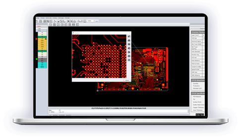
Let us look at some pictures of the UI and Menu Systems


The software also comes with a very detailed Helpfile in .pdf format
My thoughts on all of this
This is an extremely complex piece of software. It is also extremely powerful, and can thus be very very useful to all of us. The learning curve is extremely steep, but I do believe that it will be possible to learn and use it effectively.
As a Linux user, I would also like to see a Linux version, or at least an in-browser version, similar to a well-known EDA software package. The days that software should be confined to one operating system should be behind us ( at least in my personal view, I find it very frustrating that most other commercial CAD, CAM and EDA packages are actively forcing us to stay with one of the slowest operating systems available )
I also want to thank PCBPartner for giving me the opportunity to review and take this for a test drive. I would only have wanted to be more adept at actually getting value out of a great piece of software, but I believe that I will definitely get better at it over time.