18650 Cell Boost Converter

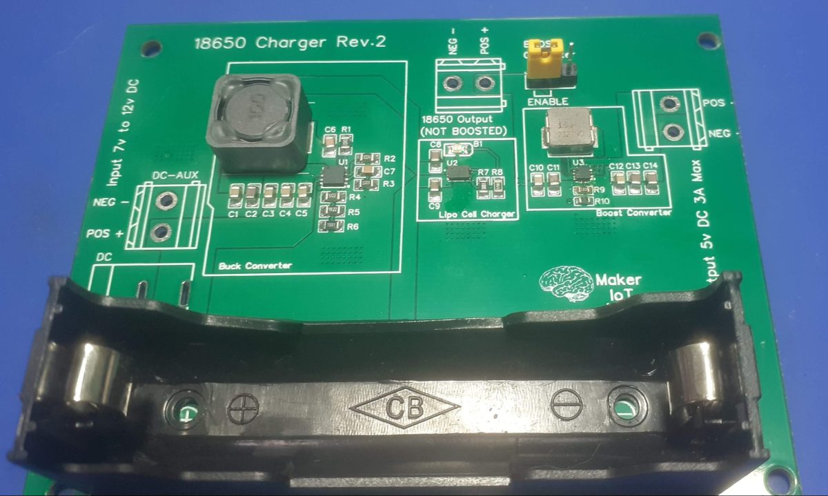
As part of an ongoing project, this tiny boost converter was designed to be used to power some of my projects, as well as become a part of a much-needed add-on circuit to the single-cell 18650 charger PCB that I designed a while ago.

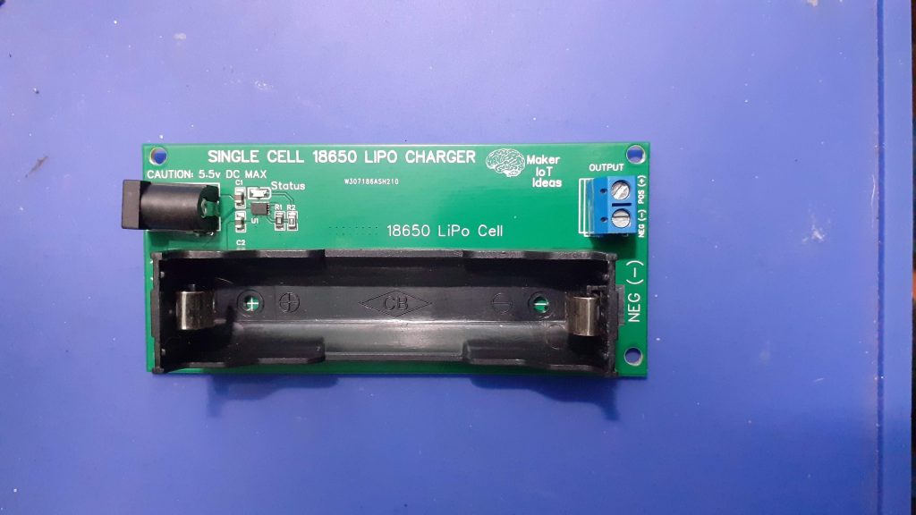
I received a lot of very useful comments from readers about the circuit below ( the single-cell 18560 Lipo charger). Most of these comments were related to adding a boost converter to the circuit, to add a little more versatility to the circuit.

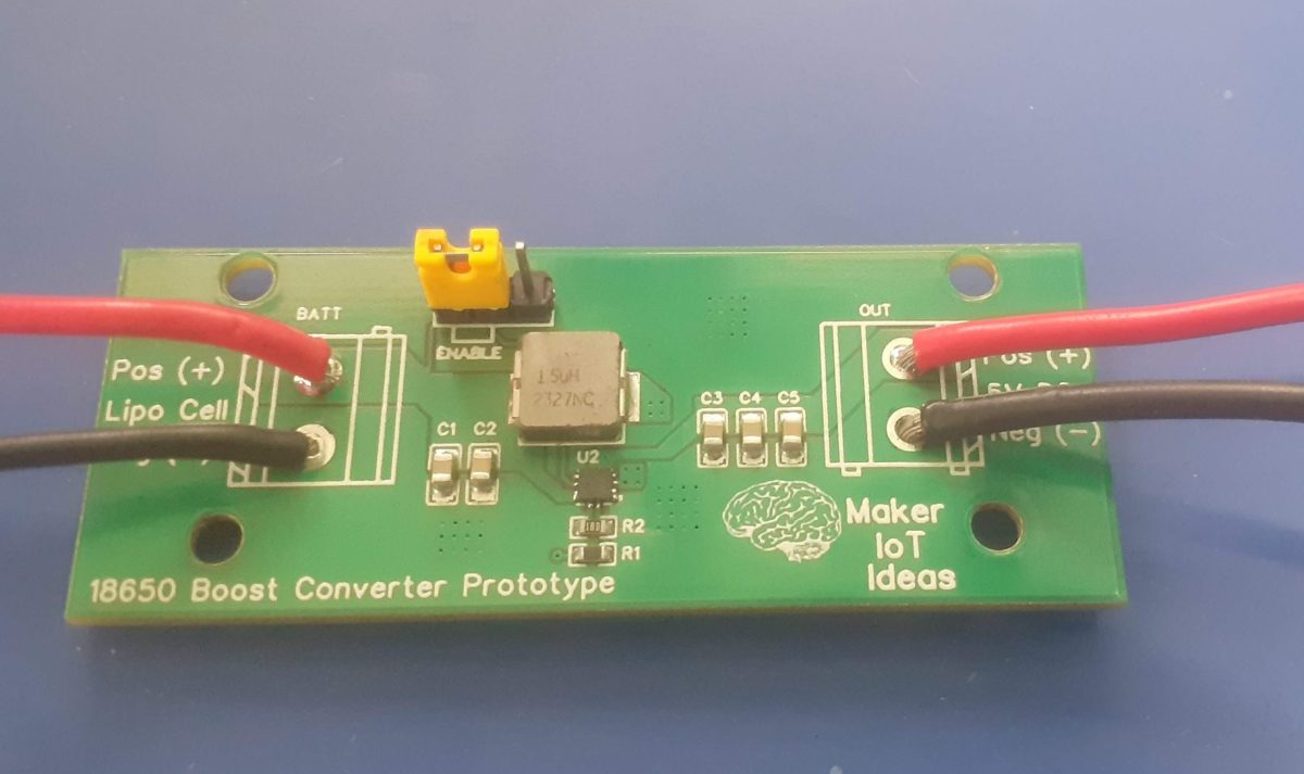
I never just add something though, and as such, this boost converter prototype was designed to test out the components and design before incorporating it into the main design. That way, I can iron out any problems before adding it to a bigger circuit.

The boost converter is based on the MP3423GG-Z, from MPS. I have decided to stay very close to their recommended application notes, so the circuit is stock standard. Another way to ensure that performance is what I want it to be, and also, to be frank, because I don’t believe I need to make any changes to the manufacturer-recommended circuit.


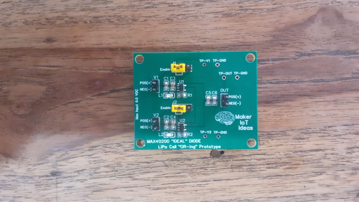
Some other comments suggested the use of “ideal diodes” at the output , in order to be able to daisy-chain the chargers. That will be addressed in a later post this month, as I am also currently testing out one of the many “ideal diode” integrated circuit chips available – in this case the MAX40200.

Being a “prototype” I did not bother with adding proper connectors to this version, as it will only be used for a short while. Soldering the supply and output wires directly to the PCB will thus be sufficient for the time being.

Design and Manufacturing

I choose PCBWay for my PCB manufacturing. Why? What makes them different from the rest?

PCBWay‘s business goal is to be the most professional PCB manufacturer for prototyping and low-volume production work in the world. With more than a decade in the business, they are committed to meeting the needs of their customers from different industries in terms of quality, delivery, cost-effectiveness and any other demanding requests. As one of the most experienced PCB manufacturers and SMT Assemblers in China, they pride themselves to be our (the Makers) best business partners, as well as good friends in every aspect of our PCB manufacturing needs. They strive to make our R&D work easy and hassle-free.

How do they do that?

PCBWay is NOT a broker. That means that they do all manufacturing and assembly themselves, cutting out all the middlemen, and saving us money.

PCBWay’s online quoting system gives a very detailed and accurate picture of all costs upfront, including components and assembly costs. This saves a lot of time and hassle.

PCBWay gives you one-on-one customer support, that answers you in 5 minutes ( from the Website chat ), or by email within a few hours ( from your personal account manager). Issues are really resolved very quickly, not that there are many anyway, but, as we are all human, it is nice to know that when a gremlin rears its head, you have someone to talk to who will do his/her best to resolve your issue as soon as possible.

Find out more here

Assembly

This PCB really would benefit from having a stencil available when you assemble it by hand. The MP3423GG-Z is super tiny, so having a guide to apply just the right amount of solder paste to the pads will go a long long way to make sure that there is no reworking needed.


All of the other components are quite manageable, being only a couple of 0805 and 0603 resistors, and an inductor. I reflow soldered everything at the same time with a hotplate. It is worth noting that I did have to remove and replace the MP3423GG-Z once during the reflow process… tiny solder bridges formed between some pins, but carefully lifting it up with a pair of tweezers, and placing it onto the pads again got rid of those completely.

We may be tempted to “leave it off the board, wait for the solder to flow and then place the component onto the molten solder…” I am not too sure about the thermal stresses that that method may or may not induce in the component… so, I prefer having it heat up slowly with the rest of the components/ and then make a quick adjustment if needed… Comments on this anyone?

Testing and final thoughts

Testing the boost converter went without any problems. It delivers a stable 5.15v DC at the output, from an input voltage of 3.3v to 4.2v. I did not test it lower than that yet… Current output seems quite stable, and the voltage does not fluctuate under load ( I tested with 2 LED COB lights, each drawing 600mA, connected in series – thus 1.2A — That is definitely the maximum current that I intend to draw from this device, although it is rated at 3A

Ripple current seems to be within the 100mV stated in the datasheet.

In summary, I believe the device performs the intended duty that i set out to design. The assembly is a bit tricky due to the small size of the MP3423GG-Z, as well as my “not-so-good” eyesight. All that aside, I am ready to advance to the next phase of the overall project – revision 2 of the Single Cell 18650 Lipo Charger.

Lipo Cell Charger Rev 2.0 – A Combination of various circuits

A few months ago, I designed, what seemed at that time like an elegant solution to solve my 18650 Lipo cell charging issues. After publishing it online, I received quite a lot of extremely useful comments, most of which highlighted some of the shortcomings of that circuit.

Well, circuit is my attempt to address some of those, and turn the circuit into something that is actually useable…

What is on the PCB

To answer this, let us start at the core and work outwards. The 18650 Lipo Cell is charged using an MCP73832T chip. This chip will charge the cell up to a nominal voltage of 4.2v DC and accept an input of up to 6.0v DC…


This presented me with my first problem, as absent-minded me accidently fried quite a few of them when accidentally connecting 12v to a PCB…

My solution to this was to add a Buck converter, based on my previous 3A Buck converter circuit(s) using the MP9943GQ from MPS. The buck converter can accept between 7v to 12v DC and output a stable 5.3v DC, saving me from frying chips, and also making it useable with most of the power supplies lying around in my lab – and it can also be used in the car at a later stage — Future project —

While that keeps the MCP73832T happy, and the 18650 cell charged, the next problem that presented itself was the nominal voltage of the 18650 cell itself, which is usually between 3.2v and 4.2v. In order for this voltage to be universally useful to me I needed a boost converter to increase the output to 5.15v.

This boost converter was built around the MP3423GG, also from MPS. This tiny little 14 pin IC provides the 5.15v that I need with ease, at a rated current of up to 3A. Ideal for powering other peripherals, like LDO regulators to power an ESP32 etc…

Manufacturing the PCB

I choose PCBWay for my PCB manufacturing. Why? What makes them different from the rest?

PCBWay‘s business goal is to be the most professional PCB manufacturer for prototyping and low-volume production work in the world. With more than a decade in the business, they are committed to meeting the needs of their customers from different industries in terms of quality, delivery, cost-effectiveness and any other demanding requests. As one of the most experienced PCB manufacturers and SMT Assemblers in China, they pride themselves to be our (the Makers) best business partners, as well as good friends in every aspect of our PCB manufacturing needs. They strive to make our R&D work easy and hassle-free.

How do they do that?

PCBWay is NOT a broker. That means that they do all manufacturing and assembly themselves, cutting out all the middlemen, and saving us money.

PCBWay’s online quoting system gives a very detailed and accurate picture of all costs upfront, including components and assembly costs. This saves a lot of time and hassle.

PCBWay gives you one-on-one customer support, that answers you in 5 minutes ( from the Website chat ), or by email within a few hours ( from your personal account manager). Issues are really resolved very quickly, not that there are many anyway, but, as we are all human, it is nice to know that when a gremlin rears its head, you have someone to talk to who will do his/her best to resolve your issue as soon as possible.

Find out more here

Assembly

The assembly of this PCB was quite challenging, to put it lightly. 3 QFN chips, with different pad spacing, and small sizes really tested my limits. Needless to say, proper equipment is a must, and even then, a very steady hand and good magnification will go a very long way towards ensuring success… Another option would definitely be to have the PCB professionally assembled…


A stencil is definitely required for this one, is only for that 14-pin boost converter IC, to make sure that the amount of solder paste is just right – and even then, it is still a challenge!

Summary

This was a challenging build that tested my assembly skills quite a bit. The circuit functions like intended. Now it is time to add some more features, like an ideal diode chip at the output, to allow for daisy chaining the lipo cells if required, as well as maybe a microcontroller to control power to the buck converter when the battery is not being charged.

MAX40200 “Ideal Diode” Lipo Cell OR-ing prototype

This short post will cover a quick experiment using the MAX40200 “ideal diode” chip. I have plans to incorporate this device into my Lipo Cell charger to allow for combining cells to provide longer run-time for my projects, as well as using mains power where available.

For this reason, I replicated the manufacturer evaluation circuit for the MAX40200 chip to test it under my typical operating conditions.

I include a very detailed description from EZ.Analog.com below

There are three primary applications for ideal diodes. One is simple reverse voltage protection for a battery-operated device. This is simply a diode in series from the battery to the application circuit. The second is as a diode OR for high-reliability redundant power supplies. Last is the same diode OR circuit, but for a selection circuit between an on-board rechargeable battery and a wall charger—just like your cell phone and many portable equipment have. Ideal diodes (such as the MAX16915) are also used for overvoltage protection on power inputs.

A designer could move from a standard diode to a Schottky diode in all three of the applications mentioned. That will be a big help with forward voltage drop with the voltage going from 1.1V for a standard diode to around 0.45V at a 1A forward current. But, an ideal diode will take you down to 85mV at that current, and they don’t cost much. Plus, they are much, much smaller. An ideal diode IC reduces power consumption, cuts voltage loss (important when coming from a low-voltage battery), and will take less PC board area. Besides, they solve a big Schottky problem. Schottky diodes have a very high reverse leakage—around 1mA for the 1A device. This leakage is not good for primary batteries, in particular. An ideal diode typically has a reverse leakage of less than 1µA over temperature.

There are three ways to get ideal. You could make your own, use a driver IC for an external FET, or use a device with an integrated FET. Driving the FET is not as easy as you might think. It’s important that the drive circuit control the forward voltage drop across the MOSFET to ensure smooth current transfer from one path to the other without oscillation. If the power source fails or is shorted, a fast turn-off minimizes reverse current transients. Implemented correctly, an ideal diode can provide front-end protection against reverse battery conditions, overvoltage transients, and inrush current. Ideal diode controller ICs, using external FETs, are available with current ratings up to 5A and voltage rating to 80V.

A great example of a complete ideal diode device is Maxim’s MAX40200, which operates from a supply voltage of 1.5V to 5.5V, handles up to 1A, and comes in a tiny 0.73mm square 4-bump WLP or a SOT23-5 package. It is thermally self-protecting and works over -40° to 125°C. When disabled, the MAX40200 blocks voltages up to 6V in either direction.

The functional diagram in Figure 1 shows a unique symbol for the internal FET. The p-channel FET has added circuitry to sense the MOSFET drain-to-source voltage and, in addition to driving the gate, keep the body diode reverse biased.

It should be noted that, unlike normal diodes, this “ideal diode” is not suited for rectifying AC. In applications where the supply is an inductively coupled 60Hz AC, conventional diodes should be used for the rectification part of the circuitry. MAX40200 is designed to be used in applications to switch between different DC sources. The chip exhibits a regulated ~20mV voltage drop up to 100mA of forward current. Above that, the forward drop increases to roughly 90mV at the maximum rated forward current of 1A. This small voltage drop will increase efficiency and significantly increase battery operation times. The IC’s dynamic response is detailed in an application note, “Static and Dynamic Behavior of the MAX40200 in a Diode ORing Application.” And, an evaluation kit, MAX40200EVKIT, is available.

For example, a AAA battery has 1Ah capacity at ~3V for two cells. If a Schottky diode drops 0.36V at 1A and our MAX40200 drops only 0.09V, the 0.27V difference yields 0.27Wh saved. So your device will run an extra quarter hour at the 1A maximum load.

The IC has a thermal shutdown temperature of about +154°C with 12°C hysteresis. if currents exceed ~500mA, care must be taken in your design to not exceed this temperature. The thermal performance of the WLP package actually exceeds that of the SOT package.

What is on the PCB ?

The PCB is very loosely based on the  MAX40200EVKIT from MAXIM. I decided to design my own version versus buying the evaluation kit because it will , at least in my opinion, give me a better understanding of the component if I use it in a design that I have slightly modified…

What modifications did I make?
Not a lot, to be honest. I added two status LED’s and enable/disable jumpers.
Except for that, the circuit is stock standard from the example provided by MAXIM.

Why did I design this PCB?

The PCB was designed to thoroughly test the Diode “Or-ing” circuit, and to determine if it would function correctly when combined with my other circuits:
In this case, it will be incorporated into my LiPo Cell charger in the near future.

Testing the design

I am quite happy to say that, at least to me, everything seems to be working as expected. I measured a reverse voltage of below 120mV at the input of a disabled device, and the voltage drop of an enabled device is also below about 120mV.

The OR-ing function works quite well, as well as running the two MAX40200 chips in parallel, i.e. with both enabled. This resulted in a sort of “hot-standby” configuration, where the load is powered by the highest “supply” and then almost seamlessly switched over to the other when the first supply is removed…

This functionality does however require some more testing, as I am currently unsure if it is within the recommended operating parameters of the device, as well as if the perceived “hot-swapover” is as seamless as it seems… for example, while powering a 5v LED COB light from a bench power supply at 5.3 v, there is a noticeable diming of the LED when the bench supply is removed and the circuit runs only on the 18650 Lipo cell, which is boosted to 5.15v… with a subsequent brightening of the LED once the bench supply is reactivated…

This leads me to believe that the dimming may only be due to slight voltage differences, and could thus confirm my idea that a hot swap over is actually possible.

Manufacturing the PCB

I choose PCBWay for my PCB manufacturing. Why? What makes them different from the rest?

PCBWay‘s business goal is to be the most professional PCB manufacturer for prototyping and low-volume production work in the world. With more than a decade in the business, they are committed to meeting the needs of their customers from different industries in terms of quality, delivery, cost-effectiveness and any other demanding requests. As one of the most experienced PCB manufacturers and SMT Assemblers in China, they pride themselves to be our (the Makers) best business partners, as well as good friends in every aspect of our PCB manufacturing needs. They strive to make our R&D work easy and hassle-free.

How do they do that?

PCBWay is NOT a broker. That means that they do all manufacturing and assembly themselves, cutting out all the middlemen, and saving us money.

PCBWay’s online quoting system gives a very detailed and accurate picture of all costs upfront, including components and assembly costs. This saves a lot of time and hassle.

PCBWay gives you one-on-one customer support, that answers you in 5 minutes ( from the Website chat ), or by email within a few hours ( from your personal account manager). Issues are really resolved very quickly, not that there are many anyway, but, as we are all human, it is nice to know that when a gremlin rears its head, you have someone to talk to who will do his/her best to resolve your issue as soon as possible.

Find out more here

Assembly

Assembly is straight forward, with not difficult to-assemble components on the PCB. I did however order a stencil, as it is just part of my work-flow.

It is however completely possible to assemble this board completely by hand using a very fine tip soldering iron.

Conclusion

Using new devices – new to me, because I have not really encountered them before – can be quite exciting, especially if things turn out the way you expected, or even better than that. The challenge from this point onwards will be to properly incorporate the MAX40200 into the proposed circuit, as well as dynamically controlling each of the two MAX40200 chips to be enabled/disabled at the right time and at the right condition.