
In part one of this series, I took a look at some of my experiments using different voltage regulators, to design and build the Remote Alarm Transceiver prototype, and also mentioned that I will be looking at a single chip logic converter solution. In this (hopefully short) post, I will take a detailed look at that logic converter chip, as well as show you how it is used.
The Logic Level Converter Chip
I have chosen the TXS0108E Bi-Directional 8-bit Logic-Level Voltage translator from Texas Instruments for this application.
Some of the features of the device is listed below:
• AEC-Q100 Qualified for Automotive Applications
– Device Temperature Grade 1: –40°C to 125°C
– Device HBM ESD Classification Level 2
– Device CDM ESD Classification Level C6
• No direction-control signal needed
• Maximum data rates
– 110 Mbps (push pull)
– 1.2 Mbps (open drain)
• 1.4 V to 3.6 V on A port and 1.65 V to 5.5 V on B
port (VCCA ≤ VCCB)
• No power-supply sequencing required – either
VCCA or VCCB can be ramped first
• Latch-up performance exceeds 100 mA per
JESD 78, Class II
• ESD protection exceeds JESD 22 (A Port)
– 2000-V human body model (A114-B)
– 1000-V charged-device model (C101)
• IEC 61000-4-2 ESD (B port)
– ±8 kV contact discharge
– ±6 kV Air-gap discharge
Datasheet description:
This device is an 8-bit non-inverting level translator
that uses two separate configurable power-supply
rails. The A port tracks the VCCA pin supply voltage.
The VCCA pin accepts any supply voltage between 1.4
V and 3.6 V. The B port tracks the VCCB pin supply
voltage. The VCCB pin accepts any supply voltage
between 1.65 V and 5.5 V. Two input supply pins
allows for low Voltage bidirectional translation
between any of the 1.5 V, 1.8 V, 2.5 V, 3.3 V, and 5
V voltage nodes.
When the output-enable (OE) input is low, all outputs
are placed in the high-impedance (Hi-Z) state.
To ensure the Hi-Z state during power-up or power-down periods, tie OE to GND through a pull-down
resistor. The minimum value of the resistor is
determined by the current-sourcing capability of the
driver.
Typical Application:

My Thoughts:
I really like the tri-state (high impedance) mode of the chip, as it allows for isolation between the different voltage level circuits, for example, If I were to communicate on a 5v SPI bus, to another device, I can for instance put the chip in Tri-state mode, and not worry about stray signals interfering from the 3v side.
On the downside, the chip is very small, which makes it a real challenge to solder by hand. On the speed side, It is also not quite as fast as my usual MOSFET based circuitry. It does however do the job it was designed for quite well.
Updated Circuit

Integrating the chip into the existing Remote Alarm Transceiver circuit is very easy, allowing us to replace almost all of the Mosfet-based Logic level converters. We do still need a few of them, as we have only 8 bidirectional channels on the TXS0108.
Schematics


Some Notes on the schematics:
A battery level monitor is connected through a voltage divider, with a MOSFET as a switch to the A0 pin. The voltage divider is set up for a 12v DC input source. The MOSFET is controlled from the D6 Pin.
The reason that I did this is, that I found some parasitic voltage leakage through the A2D converter in a previous design, reducing battery life. My hope is that by only reading battery level when the MOSFET is on, there can be an increase in battery life ( Taking into consideration that the Voltage regulators are not very efficient, it won’t really amount to a big gain unless I switch to an SMPS in the future. )
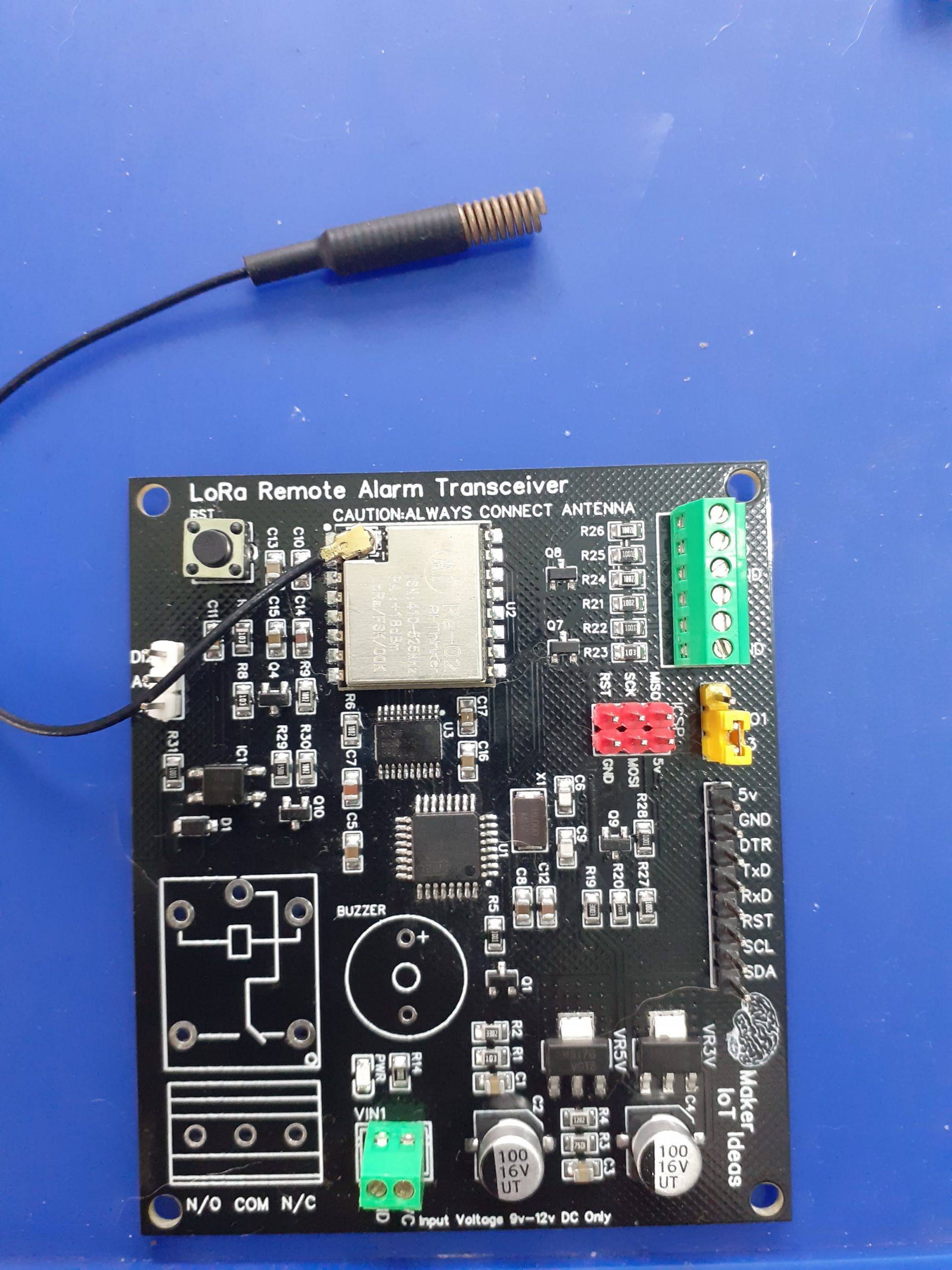
The PCB

In the picture above, we can see the completed PCB (The relay and buzzer were not populated yet)
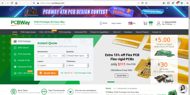
Manufacturing the PCB

This PCB was manufactured at PCBWAY. The Gerber files and BOM, as well as all the schematics, will soon be available as a shared project on their website. If you would like to have PCBWAY manufacture one of your own, designs, or even this particular PCB, you need to do the following…
1) Click on this link
2) Create an account if you have not already got one of your own.
If you use the link above, you will also instantly receive a $5USD coupon, which you can use on your first or any other order later. (Disclaimer: I will earn a small referral fee from PCBWay. This referral fee will not affect the cost of your order, nor will you pay any part thereof.)
3) Once you have gone to their website, and created an account, or login with your existing account,
4) Click on PCB Instant Quote

5) If you do not have any very special requirements for your PCB, click on Quick-order PCB

6) Click on Add Gerber File, and select your Gerber file(s) from your computer. Most of your PCB details will now be automatically selected, leaving you to only select the solder mask and silk-screen colour, as well as to remove the order number or not. You can of course fine-tune everything exactly as you want as well.
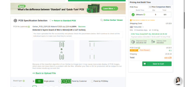

7) You can also select whether you want an SMD stencil, or have the board assembled after manufacturing. Please note that the assembly service, as well as the cost of your components, ARE NOT included in the initial quoted price. ( The quote will update depending on what options you select ).
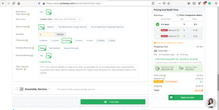
8) When you are happy with the options that you have selected, you can click on the Save to Cart Button. From here on, you can go to the top of the screen, click on Cart, make any payment(s) or use any coupons that you have in your account.
Then just sit back and wait for your new PCB to be delivered to your door via the shipping company that you have selected during checkout.