
As a companion module to my recently published 8Ch PMOD breakout board,
I decided to do a similar PCB, but with NMOS devices instead. This opens up more possibilities for proper testing and prototyping, as PMOS and NMOS devices has different use applications, and most importantly, can sometimes even be combined for a particular purpose, like an H-Bridge motor driver, for example.

What is on the PCB?
As NMOS devices function quite differently from their PMOS counterparts, it did not make sense to reuse the PMOS board, and just change the devices… although some people may be tempted to think you could…
The N Channel Mosfet basically “works in mirrored mode” from a P Channel one, and is used to do so-called ” LOW Side switching” which means that your load connects to the positive power rail, and then to the DRAIN pin of the MOSFET, with the source being connected to ground… ( It can sometimes also be used the other way around… but lets not go there now….
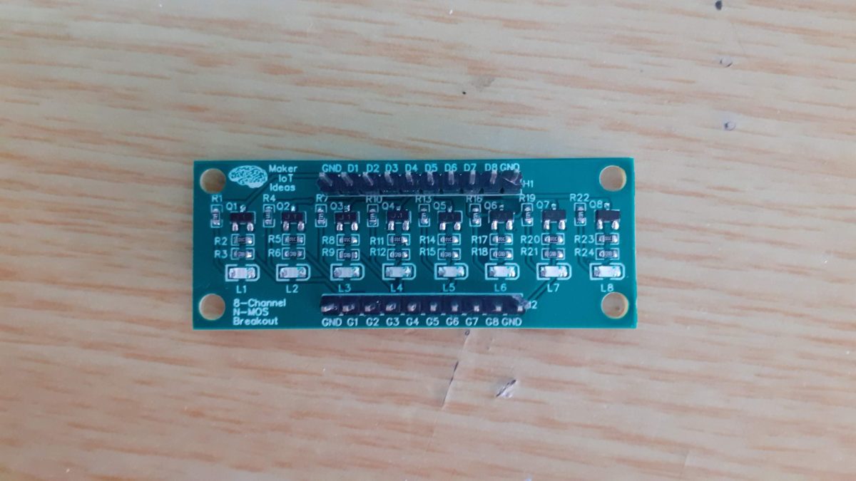
The current prototype PCB contains 8 BSS138 NMOS Mosfets, in my case, with is capable of about 800mA of current… All source pins are internally connected to ground. This forces you to use this module as a low side switch…
Two 10-way 2.54mm headers are provided, with a ground pin on Pin 1 and 10 of each of these.
The Drain pins of each NMOS device is available on the top header, labeled D1 through D8, and the Gate pins of each respective NMOS device is available on the bottom header, labelled G1 through G8.
Each gate has a pull-down resistor to ground, to keep it from flapping around, as well as a gate resistor. In my case, I selected to use a 10k pulldown, and a 1k gate resistor, as that is sufficient for my general needs…
Each NMOS device also has a LED signal indicator, to assist in visual confirmation of a specific channel’s state.

The Schematic

Using the breakout
The module is very easy to use, and as briefly mentioned above, you are only required to connect one side of your load to the positive supply rail, and the other side to the drain pin of your choice.
Connect the ground pins of the module to your ground rail.
The Gate pin, with a corresponding number to the drain you have selected, can now be connected to your GPIO of choice on a microcontroller.
Drive the pin High to switch on the load, drive it log to switch off. Easy.
Please note: While the NMOS devices used on the board can handle quite a lot of current, (800mA in the case of the BSS138), it is not recommended to try and pull too much current through a single channel. The PCB traces can safely handle about a maximum of 300 to 400mA per channel.

Manufacturing
The PCB for this project has been manufactured at PCBWay.
Please consider supporting them if you would like your own copy of this PCB, or if you have any PCB of your own that you need to have manufactured.

Example code for using the breakout (Arduino)
// Example code for 8Ch NMOS breakout
int Gate1 9;
int Gate2 10;

void setup() {
  // drive the two gate pins low to ensure NMOS devices
  // are in a positively known state at startup
  digitalWrite(Gate1,LOW);
  digitalWrite(Gate2,LOW);
  // Set gpio to output mode
  pinMode(Gate1,OUTPUT);
  pinMode(Gate2,OUTPUT);

}

void loop() {
  // Toggle the two channels in an alternating pattern
  digitalWrite(Gate1,!digitalRead(Gate1));
  digitalWrite(Gate2,!digitalRead(Gate1));
  delay(1000);

}