

This post will look at my prototype Analog front-end for the Scoppy RP2040 Oscilloscope. It is important to state right from the beginning that this circuit is one of the 5 recommended designs from the Scoppy Website. I have only moved it from the breadboard design as published, onto a PCB.
The entire circuit, with all of the original designer’s writeups, is available here
So, why use someone else’s circuit? Well, the reason for this is two-fold.
1) The circuit designer also designed the firmware, so it stands to reason that his circuit will be optimised for use with the firmware.
2) Using his circuit provides a solid reference, making it possible to test the firmware for correct operation, and later on, providing a base for my own design – if and when I do decide it is worthwhile to actually design my own.
As I already have a proper oscilloscope as well as a logic analyser, this entire exercise is purely academic, I find the Scoppy project interesting, and as such, I would like to see how it compares with my commercial products ( while also knowing that it won’t be a very fair comparison ).
With all the limitations, I am however still quite impressed at the level of use that you can get out of this very simple device. It is definitely quite useful for a beginner.
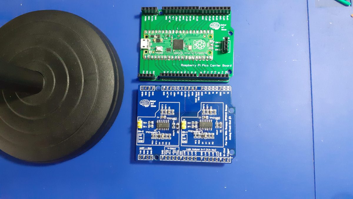
What is on the PCB, and what did I change?
The PCB is a dual-layer shield that is designed to be used with the MakerIOT2020 Raspberry Pi Pico Carrier board. The shield is directly powered by the carrier board.
The original Analog Front-End #3 circuit featured a single channel input, capable of accepting a -18.0v to 18.0v signal input.
My changes were limited to doubling up on that circuit, to provide two channels.
The Schematic

I have redrawn the original schematic, partly to make it easier to understand for myself, as well as to help me with the design of the PCB.
Lets take a look at the schematic ( by using text from the original designer)
The author makes no warranty, representation or guarantees regarding the suitability of this design for any particular purpose. Nor does the author assume any liability arising out its use and specifically disclaims any and all liability, including without limitation special, consequential or incidental damages.
All text below is quoted from here
This design builds on Design 2 and adds over and under voltage protection to the analog front end. After all, we won’t have a cheap oscilloscope if we keep frying our components!
I’m assuming here that the minimum and maximum voltages that will be applied to the input of the scope will be -18V and +18V respectively. It has been tested from -18.5V to 18.5V (two of my 9V batteries in series) but of course If you decide to use this design you are doing so at your own risk. I personally wouldn’t use Scoppy with an expensive phone/tablet just in case something unexpected goes wrong (better to use an old, obsolete phone that is no longer used for anything else) – especially when dealing with higher voltages – but of course you can do what you like.
Protecting the Op-Amp input(s)
First of all we need to protect the op-amp. In this design we’ll be using an LM324 op-amp, which is very similar to the LM358 but contains four individual op-amps rather than two. We’ll be using three of these op-amps. The reason for this will be explained later.
According to the datasheet for the LM324 the allowed input voltage range goes from -0.3V to 32V. Of course 32V is above the maximum expected voltage (18V) and so we don’t need to worry about over-voltage protection. However we do need to ensure that the voltage at the input pins don’t go below -0.3V. A schottky diode can be used to clamp the voltage to something above -0.3V (D1 in the schematic).
One thing that needs to be considered when selecting the diode is its reverse current. The 1N5817 has a very low forward voltage but high reverse current and this results in a voltage drop at the input of the op-amp (in the order of 100mV). Presumably this is because it draws current through the high value input resistor (Rg1). The 1N5711 has a much lower reverse current specification and I couldn’t discern any voltage drop when this was inserted into the circuit. However, its forward voltage (at the current expected in this part of the circuit) is very close to the minimum allowed voltage of -0.3V. To be safer I prefer to use something like a BAT46. It does result in a voltage drop of a few millivolts but the clamped voltage is more like -0.23V.
Protecting the Pico/RP2040
The Pico datasheet states that:
the ADC capable GPIO26-29 have an internal reverse diode to the VDDIO (3V3) rail and so the input voltage must not exceed VDDIO plus about 300mV
The obvious way to protect the ADC inputs (GPIO26-29) then is to simply insert a schottky diode between the ADC input and VDDIO. However, the RP2040 datasheet says that:
the voltage on the ADC analogue inputs must not exceed IOVDD ...<snip>... Voltages greater than IOVDD will result in leakage currents through the ESD protection diodes
That suggests to me that we shouldn’t be allowing current to pass (leak) through our clamping diode and into IOVDD. I could be completely wrong here – if you think so then please share your thoughts in the forum (Discussions).
Anyway, to be safe we’re going to avoid that situation by sending the current to the output of one of our op-amps (LM324-sink on the schematic). The LM324 is able to sink up to ~10mA so this should work fine if we limit the current from the main op-amp (LM324-amp in the schematic). Given that the maximum voltage expected at the output of LM324-amp is around 4.5V (Vcc – 1V) then we need a resistor of at least 120R to limit the current to 10mA (4.5-3.3 / 0.010 = 120). A 220R resistor should do fine (Rout).
And of course the reason we are using an LM324 rather than the LM358 of the previous designs is that three op-amps are required.
A 1N5817 diode (D2) is used here (rather than a BAT46 – used on the input of LM354-amp) because at the expected maximum current of 10mA the forward voltage drop of the BAT46 is higher than 300mV. The high reverse current of the 1N5817 is not such an issue here because Rout has a low value and so there will only be a small voltage drop across Rout when D2 is reverse biased.
Construction


Here are some instructions for assembling this front end on a breadboard. The pin numbers refer to the LM324 PDIP package. Refer to the schematic and breadboard image above. NB. The rail labelled 5V on the schematic is actually VSYS which of course is not necessarily 5V because it depends on how charged the battery is on your Android device.
Connect 3V3 of the Pico to the top red power rail of the breadboard. Connect VSYS to the bottom red power rail. Connect both ground rails of the breadboard to one of the GND pins of the Pico. The fuse as shown in the breadboard image is optional.
Connect the Vcc pin of the LM324 to the VSYS rail. Connect the GND pin of the LM324 to the GND rail. Don’t connect anything to the ADC pin(s) of the Pico yet.
Now we’ll configure each of the 4 op-amps of the LM324 in turn.
Op-amp 2 – Unused
Op-amp 2 (pins 5, 6 and 7 of the PDIP package) is not used so we’ll wire it up as recommended in the TI tech note – How to Properly Configure Unused Operational Amplifiers.
The voltage at the non-inverting input should be approximately VSYS/2 and the output should be the same.
Op-amp 4 – Vref
Wire up this op-amp as shown in the schematic. The voltage at the output should be approximately 1.65V.
Op-amp 3 – sink
Wire up this op-amp as shown in the schematic. The voltage at the output should be 3.3V.
Op-amp 1 – amp
Wire up this op-amp as shown in the schematic, including the under-voltage protection diode on the input (D1) and the current limiting resistor (Rout) and over-voltage protection diode (D2) on the output. Don’t connect the output to the Pico yet.
Testing and initial operation
You should now be able to safely apply any voltage at Vin1/Vin2 of between -18V and +18V. Test that the voltage at the input of the LM324 (Vampin) doesn’t go below -.3V and the voltage at the output of op-amp 2 after Rout (Vadc) doesn’t go above 3.6V.
Once you’ve confirmed that all of the op-amps have been wired correctly you can connect the output of Rout to the ADC pin of the Pico.
The author makes no warranty, representation or guarantees regarding the suitability of this design for any particular purpose. Nor does the author assume any liability arising out its use and specifically disclaims any and all liability, including without limitation special, consequential or incidental damages.
Designing the PCB


Manufacturing the PCB
The PCB for this project has been manufactured at PCBWay.
Please consider supporting them if you would like your own copy of this PCB, or if you have any PCB of your own that you need to have manufactured.

Assembly
The PCB was assembled with help of a stencil to ease and speed up the solder paste application. The components were then hot-air soldered.
As this is only a prototype, I chose to only place 2.54mm header pins on pins that are required for operation, as well as all the ground pins, to ensure a proper ground plane.


Conclusion
This was quite an interesting project. While everything works as expected, resolution and frequency are limited. ( of course, it is…) The project is however still useful, and will definitely give you some useful results in a pinch.
The logic analyser is by far more useful, but once again, a commercial device will be way more accurate and useful for professional use. Hopefully, the designer will add some protocol filters etc in future.
This device will not replace a proper oscilloscope or logic analyser, but it will definitely give enough accuracy and resolution on low-frequency applications to satisfy some of the basic needs of a beginner or student just starting out with electronics.
It is also important to note that you should be safe, and not try to connect this to high voltages etc. Also, don’t connect this to your expensive phone or tablet, use an old one instead, as accidents may happen, and we don’t want to damage our valuable handheld devices…