
I had a need to build a reliable LoRa device, in order to do some testing regarding range etc, for an upcoming project on a friend’s farm. The device needs to be ultra-cheap to manufacture, as well as little power as possible. To achieve this, I decided on using the RA-02 ( From AI Tinker, not sponsored) as well as an ATMEGA328P, which consumes very little current when put to sleep… ( The radio will be on standby the whole time though..)
Building this with a standard Arduino, or another ATMEGA powered development board can be quite messy ( as the picture below shows… )
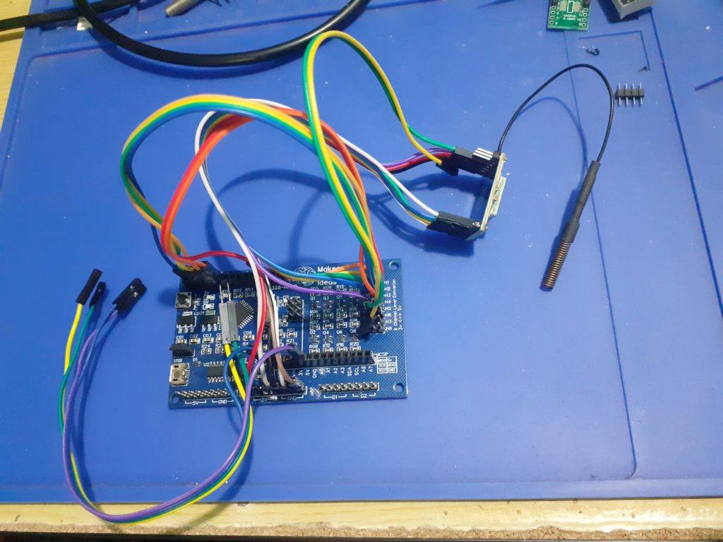
A standard Arduino will be even worse, as you need level conversion on the SPI pins, due to the fact that the RA-02 is a 3.3v device, with the GPIO, not being 5v tolerant (Yes, this is true, some other posts on Youtube and similar conveniently leave out this very important little caveat… )
This problem thus warranted a dedicated custom PCB, to be designed in stages, and thoroughly tested of course… And while doing that, I needed to design something that was modular and useable.
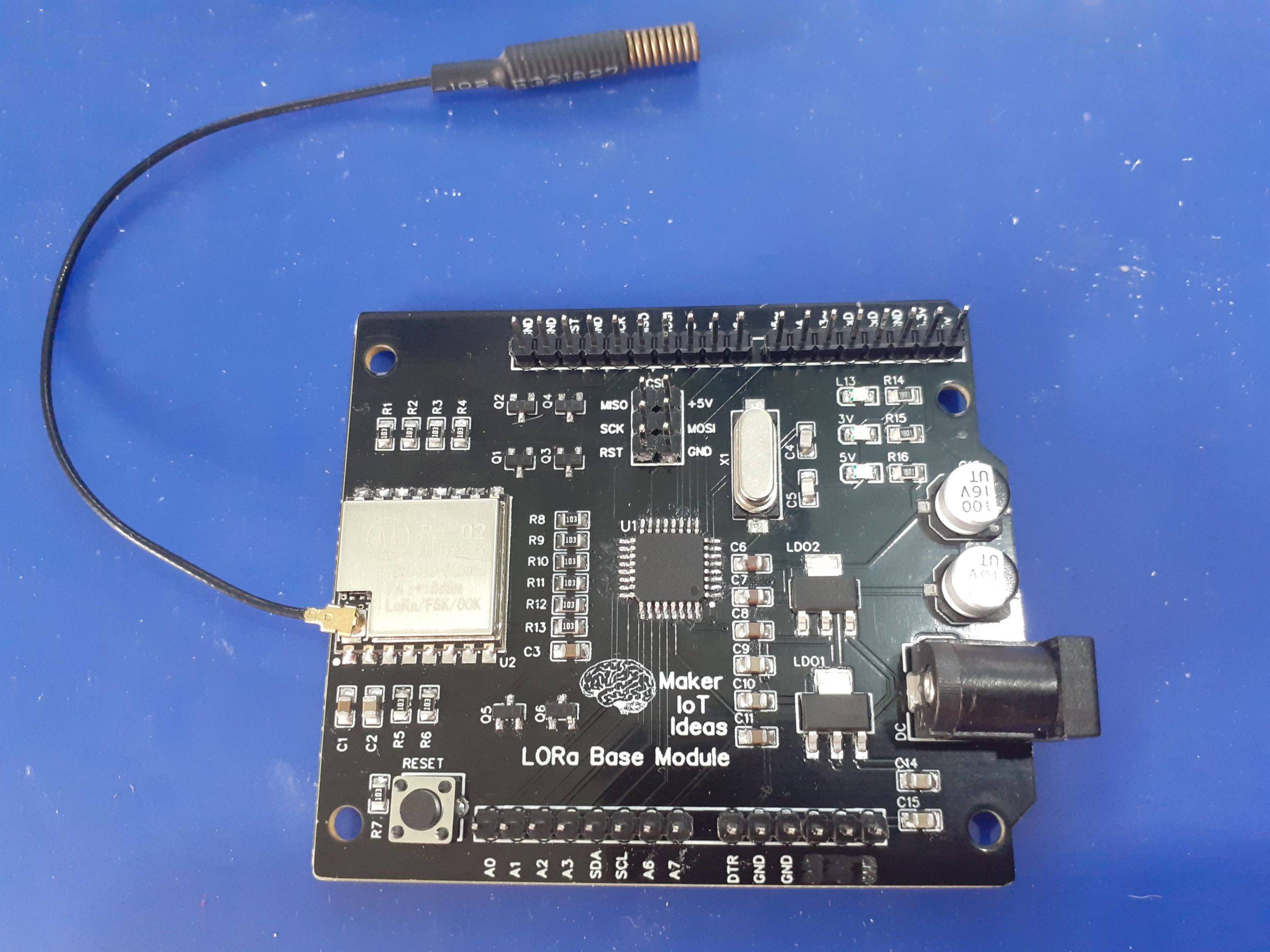
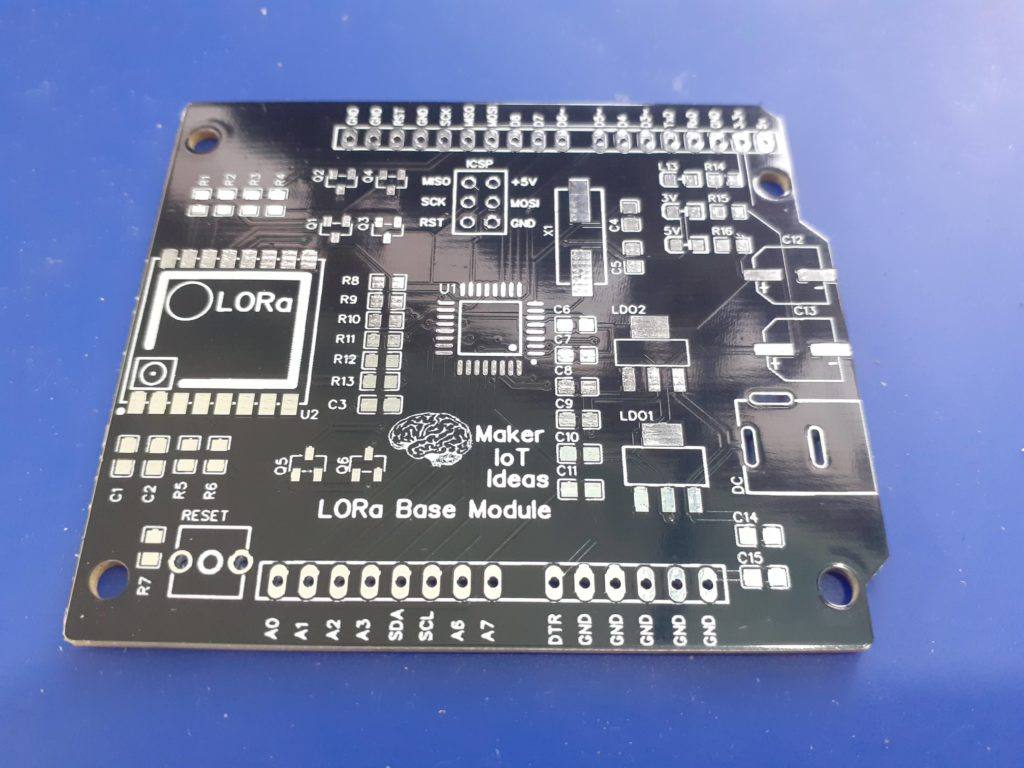
I came up with the following design, as a stage one prototype:
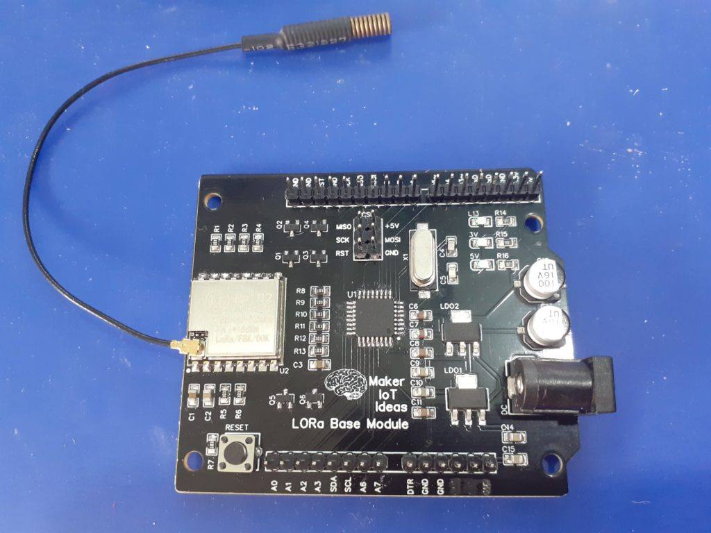
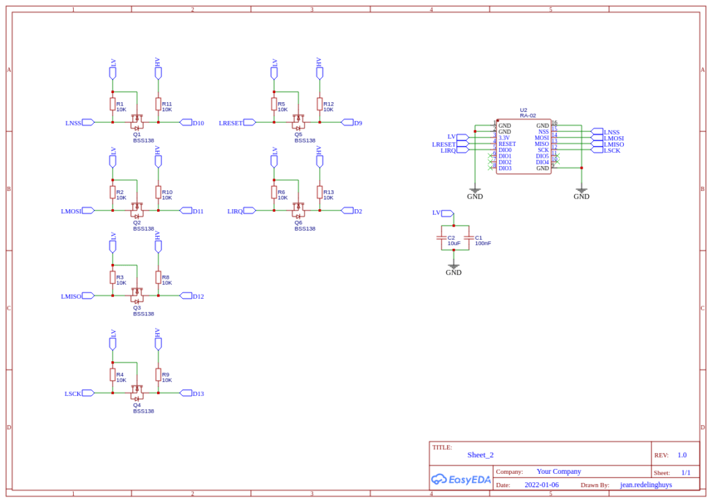
The PCB is basically an Arduino Nano style PCB ( as far as IO is concerned ), with level conversion on the SPI lines ( SCK, MISO, MOSI, SS) as well as a Lora reset and IRQ pin ( which will be essential to wake up the processor later ).
As the prototype will mostly be used in the lab, with some outdoor tests later, provision was not made for battery charging circuitry. Two LDO regulators, 5v and 3.3v provide power to the ATMEGA328P and RA-02 from a DC input of 7.5 to 12v.
Level conversion is fixed at bi-directional 5v to 3v logic levels.
All unused GPIO’s are broken out onto headers.
Code can be uploaded to the MCU via ICSP or a USB-to-serial converter, as I did not add those on board, to save space and power later.
Control Pins are as follows:
| RA-02 Module | ATMEGA328P |
| SCK | D13 |
| MISO | D12 |
| MOSI | D11 |
| NSS | D10 |
| RESET | D9 |
| IQR(DIO0) | D2 ( Interrupt 0 ) |
| DIO1 | Not broken out on stage 1 Prototype |
| DIO2 | Not broken out on stage 1 Prototype |
| DIO3 | Not broken out on stage 1 Prototype |
| DIO4 | Not broken out on stage 1 Prototype |
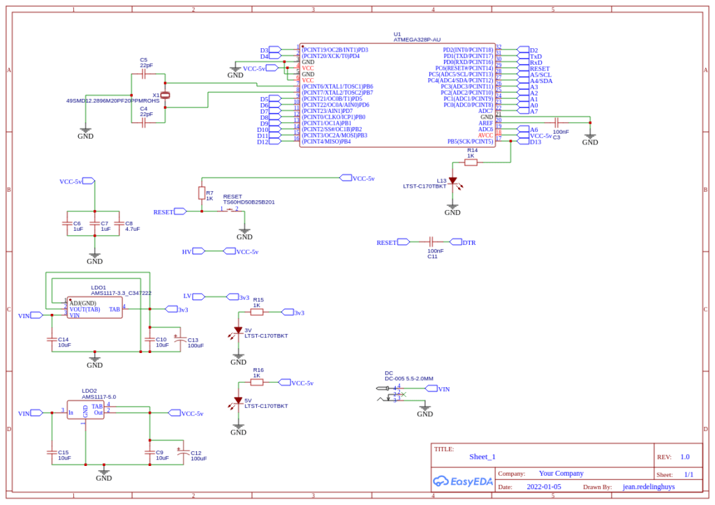
The Schematic diagram are listed below
Software
The board is compatible with the LoRa library from Sandeep Mistry. Other libraries may work as well but were not tested yet.
A very basic test sketch follows below:
Note that this sketch does not have any power-saving. It is purely used to do a very basic radio test…
More detailed code will be released in later stages of the project ( more on that later )
#include <SPI.h>              // include libraries
#include <LoRa.h>

const int csPin = 10;          // LoRa radio chip select
const int resetPin = 9;       // LoRa radio reset
const int irqPin = 2;         // change for your board; must be a hardware interrupt pin

byte msgCount = 0;            // count of outgoing messages
int interval = 2000;          // interval between sends
long lastSendTime = 0;        // time of last packet send

void setup() {
  Serial.begin(9600);                   // initialize serial
  while (!Serial);

  Serial.println("LoRa Duplex - Set spreading factor");

  // override the default CS, reset, and IRQ pins (optional)
  LoRa.setPins(csPin, resetPin, irqPin); // set CS, reset, IRQ pin

  if (!LoRa.begin(433E6)) {             // initialize ratio at 433 MHz
    Serial.println("LoRa init failed. Check your connections.");
    while (true);                       // if failed, do nothing
  }

  LoRa.setSpreadingFactor(8);           // ranges from 6-12,default 7 see API docs
  Serial.println("LoRa init succeeded.");
}

void loop() {
  if (millis() - lastSendTime > interval) {
    String message = "LoRa TEST";   // send a message
    message += msgCount;
    sendMessage(message);
    Serial.println("Sending " + message);
    lastSendTime = millis();            // timestamp the message
    interval = random(2000) + 1000;    // 2-3 seconds
    msgCount++;
  }

  // parse for a packet, and call onReceive with the result:
  onReceive(LoRa.parsePacket());
}

void sendMessage(String outgoing) {
  LoRa.beginPacket();                   // start packet
  LoRa.print(outgoing);                 // add payload
  LoRa.endPacket();                     // finish packet and send it
  msgCount++;                           // increment message ID
}

void onReceive(int packetSize) {
  if (packetSize == 0) return;          // if there's no packet, return

  // read packet header bytes:
  String incoming = "";

  while (LoRa.available()) {
    incoming += (char)LoRa.read();
  }

  Serial.println("Message: " + incoming);
  Serial.println("RSSI: " + String(LoRa.packetRssi()));
  Serial.println("Snr: " + String(LoRa.packetSnr()));
  Serial.println();
}
Future Plans
Future plans for this project include the following:
– Integration of a LiPo battery charging module, with a boost converter, to enable the device to run on battery power.
– Integration with an ESP32 or similar, to build a simple GATEWAY device
– CAN-BUS controller integration, to allow for adding multiple sensors to one radio module
– IO card, with galvanically isolated inputs, as well as Relay outputs, for remote control and monitoring applications.
The PCB can be ordered, or the design files downloaded ( a free download ) from my Projects page at PCBWay soon…

This PCB was manufactured at PCBWAY. The Gerber files and BOM, as well as all the schematics, will soon be available as a shared project on their website. If you would like to have PCBWAY manufacture one of your own, designs, or even this particular PCB, you need to do the following…
1) Click on this link
2) Create an account if you have not already got one of your own.
If you use the link above, you will also instantly receive a $5USD coupon, which you can use on your first or any other order later. (Disclaimer: I will earn a small referral fee from PCBWay. This referral fee will not affect the cost of your order, nor will you pay any part thereof.)
3) Once you have gone to their website, and created an account, or login with your existing account,
4) Click on PCB Instant Quote
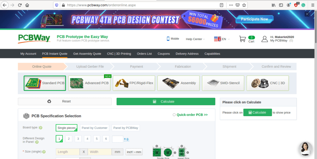
5) If you do not have any very special requirements for your PCB, click on Quick-order PCB
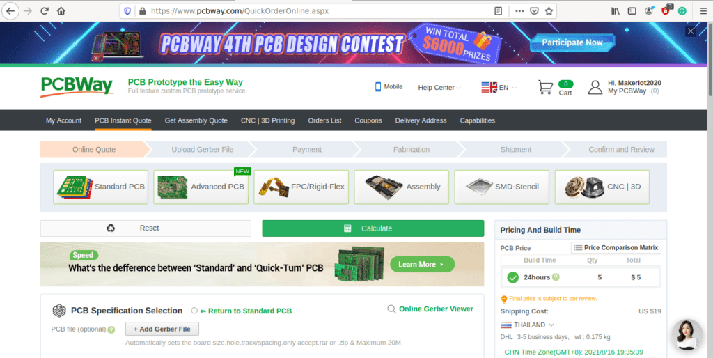
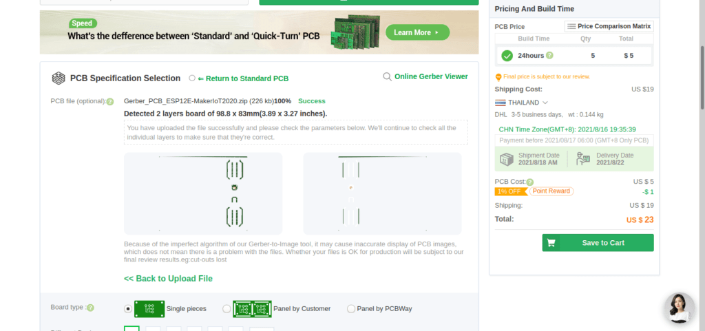
6) Click on Add Gerber File, and select your Gerber file(s) from your computer. Most of your PCB details will now be automatically selected, leaving you to only select the solder mask and silk-screen colour, as well as to remove the order number or not. You can of course fine-tune everything exactly as you want as well.
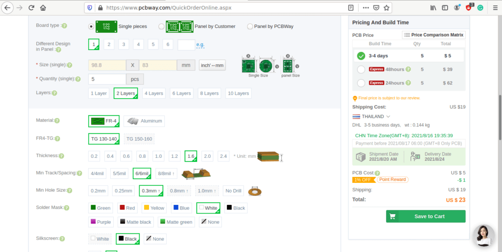
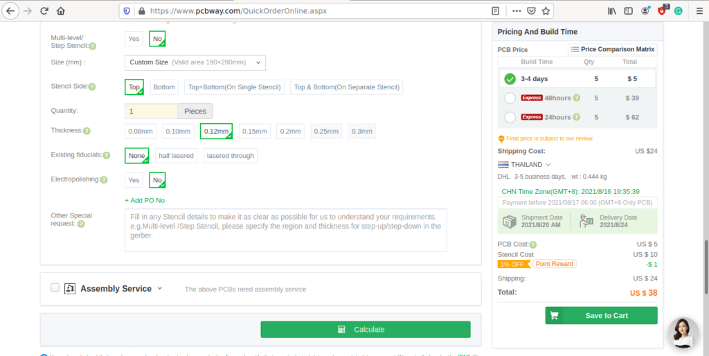
7) You can also select whether you want an SMD stencil, or have the board assembled after manufacturing. Please note that the assembly service, as well as the cost of your components, ARE NOT included in the initial quoted price. ( The quote will update depending on what options you select ).
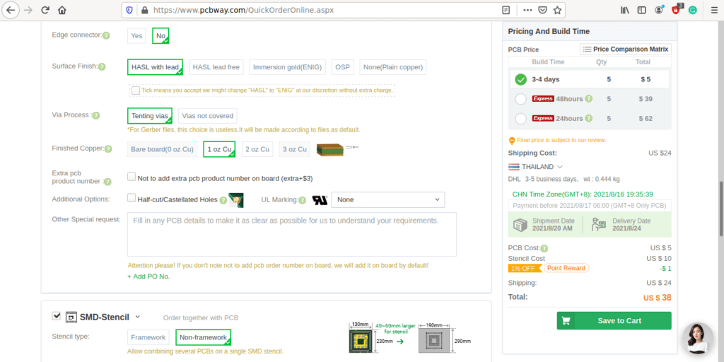
8) When you are happy with the options that you have selected, you can click on the Save to Cart Button. From here on, you can go to the top of the screen, click on Cart, make any payment(s) or use any coupons that you have in your account.
Then just sit back and wait for your new PCB to be delivered to your door via the shipping company that you have selected during checkout.