INPUT And Monitor Shield for LoRa Base Module
Introduction
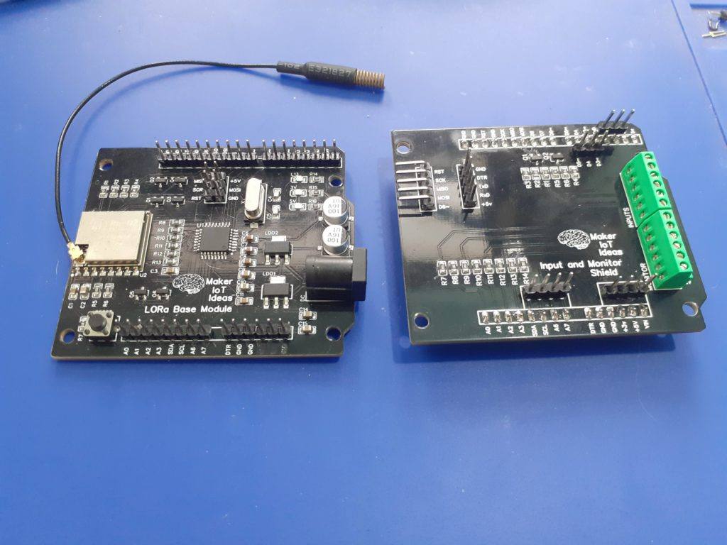
This is a straightforward project compared to my usual PCB projects. It is one of a series of designs towards completing my LoRa monitoring system, that I plan to use on the farm to monitor various areas, such as intrusion detection, battery levels etc.
The shield was designed to fit on top of the first LoRa Base Module. It was designed to allow easy, neat connections to Infrared Beam sensors, XYC-WB-DC Motion Detector, as well as to monitor the battery levels at the Solar power inverter (the farm is completely off-grid).
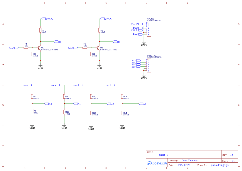
The Motion Sensor provides a +3v signal that goes high on motion detection, while the Infrared Beam Sensor provides a relay contact that can be used to provide a similar voltage signal. As I prefer to use pull-up logic on my inputs, I decided to implement a simple transistor circuit where the input will switch the base of the transistor, which in turn will pull the input to signal ground when switched on. This circuit uses the S8050 transistor, with the base pulled down to signal ground via a 10k resistor to prevent floating, and a current limiting resistor of 1k to 1k8 on the base. The collector, as well as the D7 and D8 GPIO pins on the LoRa Base Module, is pulled High to Vcc5v via a 10k resistor.
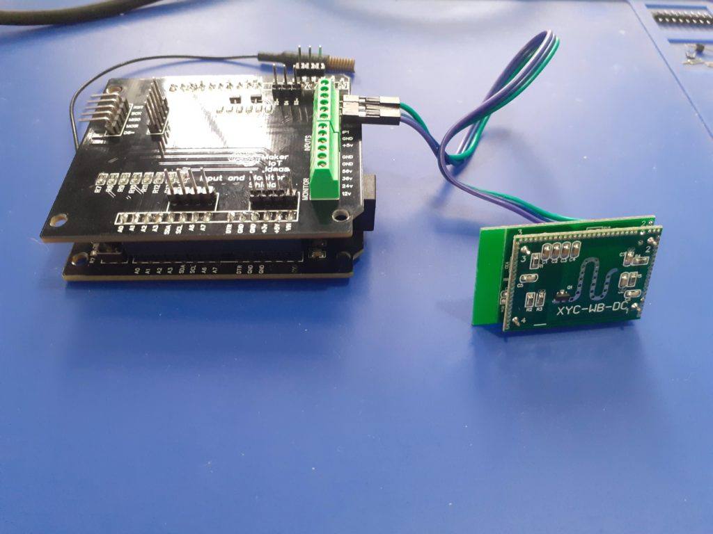
Voltage monitoring is done with the ADC on the LoRa Base Module, with each of the 4 battery levels ( 12v, 24v,36v, and 56v) being connected to the relevant ADC channel via a resister-divider network to lower the respective voltage to a level between 0 and 5v. ( This was done as the ADC on the ATMEGA328p can only handle a maximum voltage of 5.0v )
The resistors were chosen to give a slightly bigger input voltage range, to accommodate for fluctuations from the solar charger ( It can sometimes go up to 65v on a very bright sunny day ). I decided to not add any current limiting resistors directly onto the PCB, as they are definitely going to be bulky. They will instead be attached externally, to suitable heatsinks, etc…
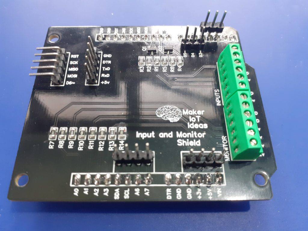
As this PBC is still in the prototype stage, and my LoRa Monitoring device will definitely go through quite a few modifications in future, I provided access to all unused GPIO pins via separate headers on the shield. Most notably the SPI Header, used for programming the ATMEGA328P MCU, or connecting other SPI devices ( I am working on a CAN bus addon for the device, to save on the number of physical radio nodes that needs to be installed), The UART Header, as well as I2C, A6, A7 and additional Digital IO Pins (D3~, D4, D5~).
In the photo above you will notice an additional header on the UART pins, This was added to assist me with debugging on the logic analyser, as I had a slight issue with waking up the ATMEGA328P, and getting it to send events via LoRa. It would wake up, print status messages through the UART, but never do the actual LoRa part! That has now been fixed, and the header removed…
The schematic diagram for the shield is below. As you will see, it is very uncomplicated indeed.
Software and Libraries
The LoRa Base Module has been designed to use the LoRa Library from Sandeep Mistry. Further versions of this PCB will also directly support the RadioLib Library from JGromes.
A reminder :
The RA-02 Module (SX1278) connections to the ATMEGA328p is as follows:
NSS to D10 (CE)
MOSI to D11 (MOSI)
MISO to D12 (MISO)
SCK to D13 (SCK)
RESET to D9
DIO0 to D2 ( We need a hardware Interrupt pin ).
DIO1 to DIO5 was not broken out on the current version of the LoRa Base Module
There is also no direct access to pins D10, D9 and D2 either on the LoRa Base Module or on the Input and Monitor Shield.
If you do decide to hack the device and add access to any of the non broken out pins, please remember to use a logic level converter between the ATMEGA328 and the SX1278, as they operate at different voltages, and the SX1278 is not 5v tolerant on any of the IO Pins!
You can order this shield from PCBWay by clicking here

This PCB was manufactured at PCBWAY. The Gerber files and BOM, as well as all the schematics, will soon be available as a shared project on their website. If you would like to have PCBWAY manufacture one of your own, designs, or even this particular PCB, you need to do the following…
1) Click on this link
2) Create an account if you have not already got one of your own.
If you use the link above, you will also instantly receive a $5USD coupon, which you can use on your first or any other order later. (Disclaimer: I will earn a small referral fee from PCBWay. This referral fee will not affect the cost of your order, nor will you pay any part thereof.)
3) Once you have gone to their website, and created an account, or login with your existing account,

4) Click on PCB Instant Quote
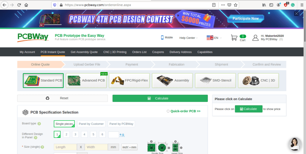
5) If you do not have any very special requirements for your PCB, click on Quick-order PCB
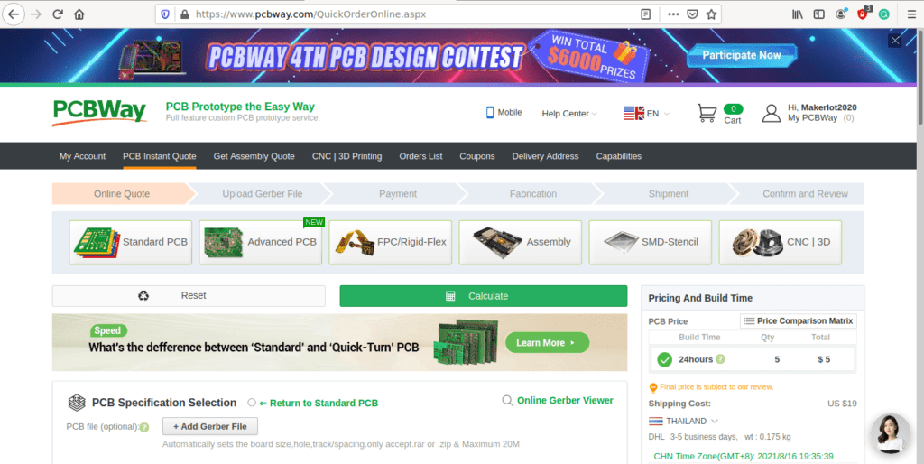
6) Click on Add Gerber File, and select your Gerber file(s) from your computer. Most of your PCB details will now be automatically selected, leaving you to only select the solder mask and silk-screen colour, as well as to remove the order number or not. You can of course fine-tune everything exactly as you want as well.
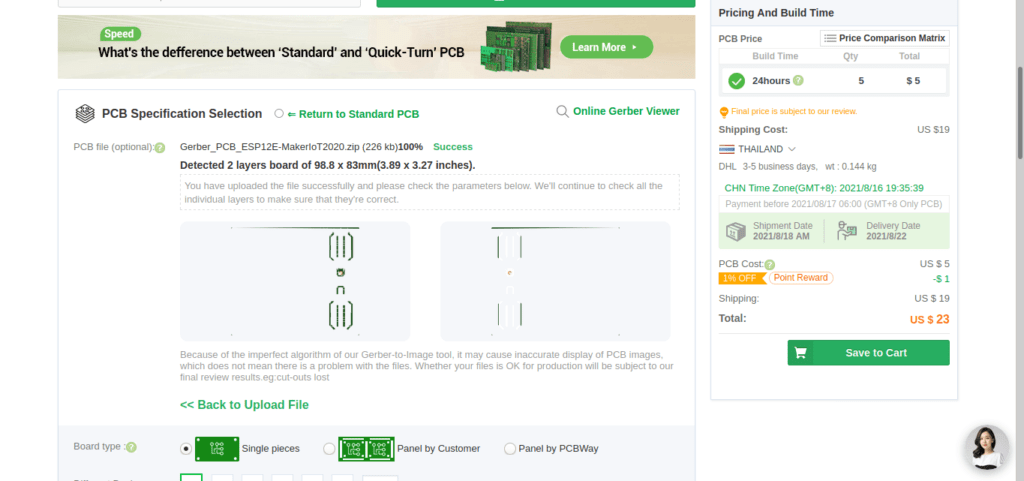
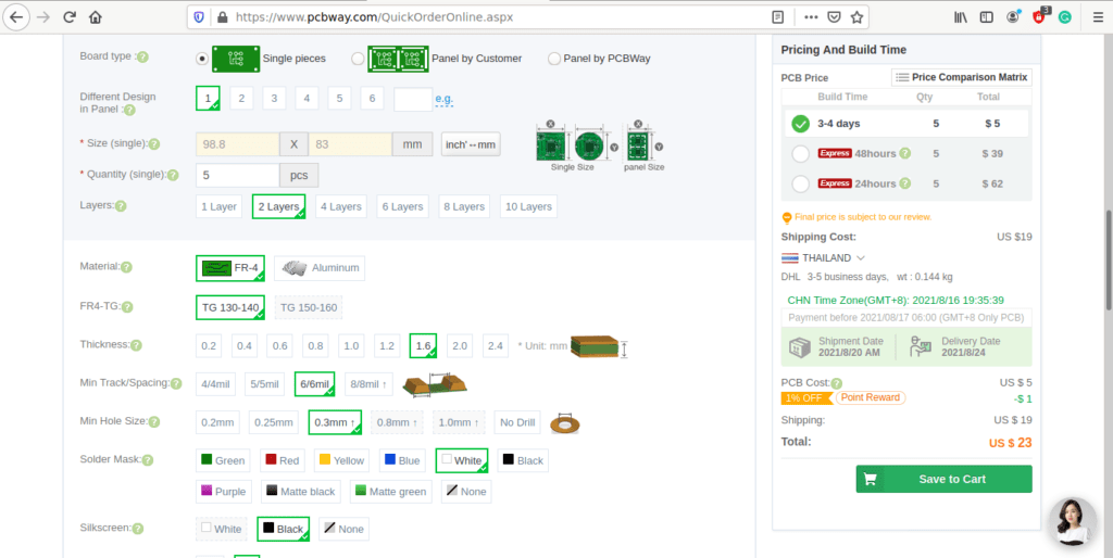
7) You can also select whether you want an SMD stencil, or have the board assembled after manufacturing. Please note that the assembly service, as well as the cost of your components, ARE NOT included in the initial quoted price. ( The quote will update depending on what options you select ).
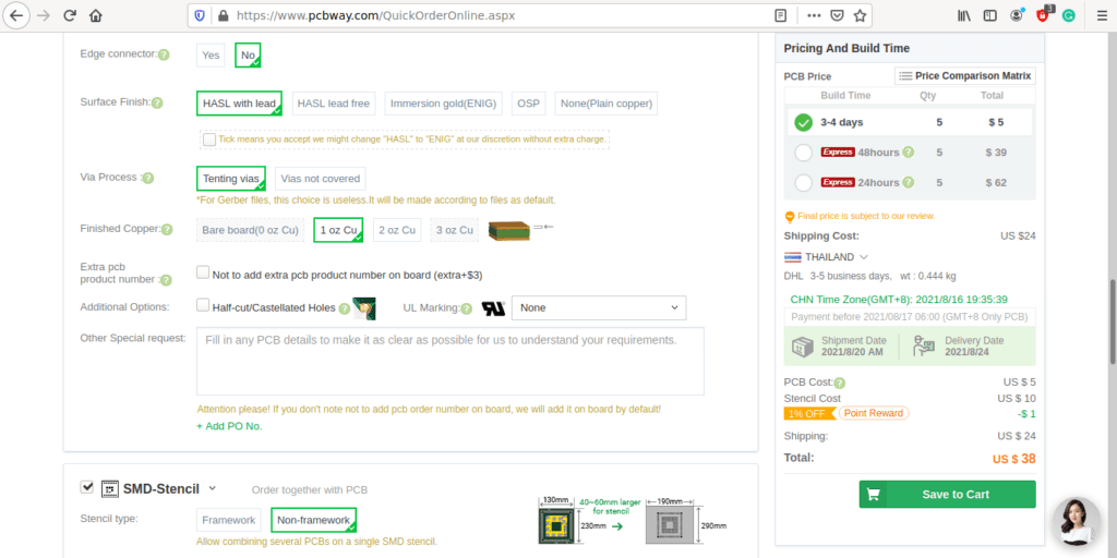
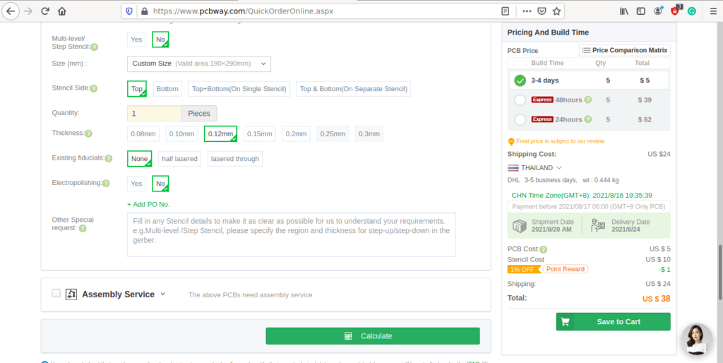
8) When you are happy with the options that you have selected, you can click on the Save to Cart Button. From here on, you can go to the top of the screen, click on Cart, make any payment(s) or use any coupons that you have in your account.
Then just sit back and wait for your new PCB to be delivered to your door via the shipping company that you have selected during checkout.

