The Assembly of the ATTiny1616 Can Bus Controller PCB will be covered in this post. This PCB took quite a bit of time, due to having a real-world job that takes up an extreme amount of my time.
Enough of that, let’s get started
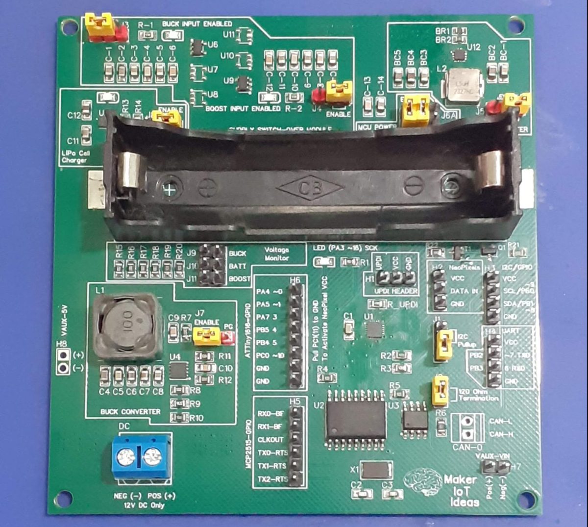
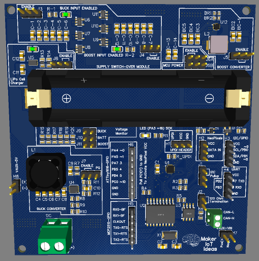
The PCB
The PCB is a double layer, with mostly SMD components, and as mentioned in the initial post, broken up into functional blocks to make testing easier. I will also take the time to mention some performance and problem issues that I have encountered during the testing phase here are well
These include: – a buck converter power supply module to provide 5v DC. – a single-cell lipo cell charger circuit – an ideal diode supply or-ing circuit – a boost converter – various jumpers, so enable/disable certain parts of the circuit – microcontroller and logic circuits
The bare PCB
All of the circuit modules mentioned have been covered in detail in previous posts, so I will only briefly review some of them here to highlight some changes I have made to the original circuits.
The ideal diode supply or-ing circuit has been modified to use 3 ideal diode chips in parallel per “channel”. This is “experimental” from my point of view since I am unsure if it would actually perform as expected. I had to do this due to experiencing great difficulty in obtaining a suitable high-current component at a reasonable cost and in a suitable footprint.
This question remains unanswered, as I encountered a double whammy with no stock issue forcing me to use one device per channel. I shall update the performance of this experiment soon when I receive the back-ordered components.
The performance of the boost converter can at best be described as temperamental. This is definitively an assembly issue on my side, as the controller chip is tiny (approx. 2mm x 2mm with 14 leads), and hand assembly of this with a stencil and hot-plate reflow almost always results in the need to hot-air rework and then possibly damaging the chip with heat or other issues.
I am currently investigating an alternative chip to use in future versions of the PCB to remove this issue. When the circuit works, it is rock solid and gives great performance. Maybe someone from Microchip (#not sponsored) can give some advice here…
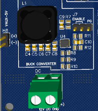
The Buck converter performs solidly as usual, great little device! No complaints there as usual.
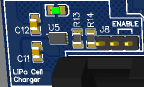
The Lipo-cell charger performs as expected, with no issues to report.
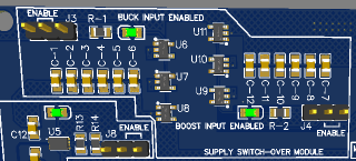
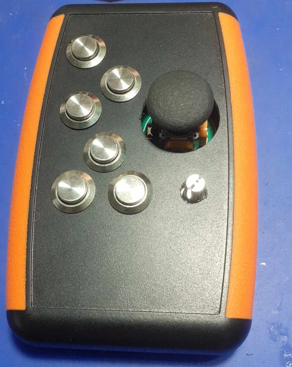
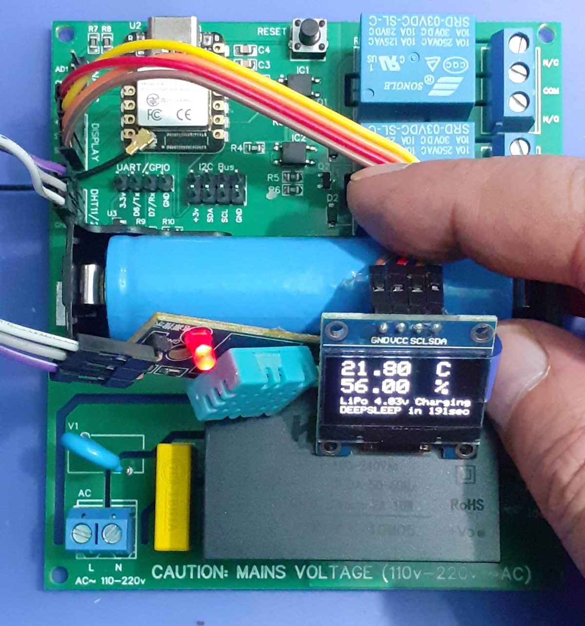
As seen in the picture above, I have placed yellow jumpers to make it easy to enable/disable parts of the circuit to aid in testing and debugging. These help quite a lot.
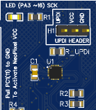
The ATTiny 1616 is solid, as can be expected, and functions exactly as expected. Some users would have to replace the R_UPDI resistor with a 0ohm link, depending on which UPDI programmer you use. Since I use my own custom-made UPDI Programmer as recommended in a circuit by Spence Konde/Dr Izzy on his excellent megatinyCore documentation site, I have no issues with UPDI.
The Can-Bus hardware functions as expected, with no issues to report.
There is also an error on the silkscreen, Pin_PC1 should be pulled HIGH to activate the VCC line for the neoPixel strip, NOT LOW as printed on the silkscreen.
Manufacturing the PCB
I choose PCBWay for my PCB manufacturing. Why? What makes them different from the rest?
PCBWay‘s business goal is to be the most professional PCB manufacturer for prototyping and low-volume production work in the world. With more than a decade in the business, they are committed to meeting the needs of their customers from different industries in terms of quality, delivery, cost-effectiveness and any other demanding requests. As one of the most experienced PCB manufacturers and SMT Assemblers in China, they pride themselves to be our (the Makers) best business partners, as well as good friends in every aspect of our PCB manufacturing needs. They strive to make our R&D work easy and hassle-free.
How do they do that?
PCBWay is NOT a broker. That means that they do all manufacturing and assembly themselves, cutting out all the middlemen, and saving us money.
PCBWay’s online quoting system gives a very detailed and accurate picture of all costs upfront, including components and assembly costs. This saves a lot of time and hassle.
PCBWay gives you one-on-one customer support, that answers you in 5 minutes ( from the Website chat ), or by email within a few hours ( from your personal account manager). Issues are really resolved very quickly, not that there are many anyway, but, as we are all human, it is nice to know that when a gremlin rears its head, you have someone to talk to who will do his/her best to resolve your issue as soon as possible.
Due to the size of some of the components on this PCB, a stencil is compulsory for hand assembly of this PCB, or even better, have it professionally assembled by your PCB manufacturer. It will save you a lot of headaches during assembly
The stencil that I got from PCBWAy made things so much easierThe assembled PCB, without CAN connector and Lipo Cell
Conclusion
This project took way longer than initially planned, due to many issues including logistics, component availability, the need to rework some areas of the board, and being super busy at my day-job. The firmware is still a work in progress, with bits and pieces of code floating around, hacked together to test basic functionality but nothing else.
I hope to complete this project very shortly, and after a final revision of the hardware, to get rid of some issues that bug me, to have a very useable piece of equipment to finally install in my car as planned from the very beginning
Over the last few months, we have been working on several prototypes, and some of our regular visitors may recognise some parts of this PCB. But let us begin by telling you what this is about.
As many of you may know, we have already designed several Can-Bus-related development boards, including one based on the ATTiny1616… So why the repeat then? Well, in some of my previous projects, I hinted at combining a buck converter, boost converter, lipo cell charger and Ideal Diode circuit into one PCB. I did at that time not tell you why.
To make a long story short, this project will eventually be used in my car, to provide more modern cabin lighting, which is quite a bit more than the standard on-or-off and on-when-open-the-door, off-when-close-the-door type of thing…
I own an old Honda City that I use mainly for a run-around to and from the farm, as well as seeing clients… Roads are bad, and this older car (actually quite old – 22 years) is the most cost-effective, in terms of being able to repair by myself, and not be worried about it if it gets a bit abused.
Unfortunately, the technology in the car is dated… a single yellowish cabin light right in the centre of the cabin – and not bright at all. Having to use the car at night, and then frequently scratching around in equipment bags when arriving at a client, becomes a pain with bad light… So I have decided to give it a bit of an upgrade and add CAN-bus-controlled NEO-Pixels to the cabin. For now, let’s say three sets, left, right and centre of the cabin. I also prefer a red light at night over white, especially if I have to drive again soon afterwards – a simple remnant from my days in the military, where it became quite clear how white light can temporarily damage your night vision.
NeoPixels can also be dimmed/brightened and seem relatively inexpensive.
Let us take a closer look at exactly what I want to do…
Powering the module
For the sake of clarity, this particular module will be installed front and centre in the cabin, just behind the rearview mirror. It will control two sets of 8 neopixels ( or up to 12 per module ) on two separate PCBs, which will cover the driver and front passenger area of the cabin.
The module will be powered by the vehicle’s 12v battery, as well as from a single 18650 Lipo cell. This means that we would need some clever tricks, in the form of a buck converter to step down the 12v to 5v, a way to monitor and recharge the lipo cell, a boost converter to boost the lipo cell voltage back up to 5v as well as a voltage “OR-ing circuit” to prevent reverse charging the lipo cell etc…
In its current state, the PCB is to be considered a test rig, since I have quite a few unknown variables that need to be thoroughly tested before actually installing this thing into a vehicle.
These are : 1) I would like to know if the ideal diode chip that I used functions well when used in a parallel setup, The reason for that is, that a single chip is capable of just about 1A of current… thus, in my reasoning, placing 3 in parallel would give me the 3A capability that I require – Let’s see if it does… I could also not get hold of a suitable 3A capable ideal diode chip that was cost-effective, or did not have some strange MOQ or other logistics issues ( Yeah, seems like getting some stuff in SE Asia is difficult unless you are willing to pay unnecessary “special” charges and import duties etc … Element14 ( not sponsored) seems to have a limited selection of ideal diode solutions, but their pricing is good, and there are minimum hassles with shipping etc… I don’t bother with the other two big suppliers, D…. and M…. as they have too much red tape for a hobbyist to navigate to make it cost-effective to shop from them.))
2) Providing that the ideal diode solution does work as expected ( on the PCB) – having tested it on a breadboard seems to be working fine, there is the issue of monitoring the lipo cell, getting it charged, controlling the boost converter to provide power when needed etc…
All of this means that all the separate circuit modules on the PCB can be enabled or disabled by jumpers, and later, if all works as expected, maybe by another controller PCB… Who knows?
Getting back to power the PCB, I have used my standard buck converter circuit, based around the MP9943. This circuit seems to be very reliable, provides enough current, and is cost-effective.
I have also provided an auxiliary voltage output ( 5v) and some telemetry and control capability to the buck converter circuit, in the form of an enable-disable jumper, and the PG signal from the chip, to maybe be interfaced with a microcontroller later.
Charging the Lipo Cell
Once again, I made use of an existing circuit, with which I have had a lot of success in the past. This circuit, based on the MCP73832 from Microchip ( not sponsored) served me quite well in previous projects, and is once again, cost-effective and easy to implement. One negative is that they do seem to be a bit finicky, and not extremely robust – but when they work, they excel at it…
Once again, I decided to provide control logic to enable or disable this part of the circuit completely if needed.
Supply “OR-ing” circuit
This is the most experimental part of this entire circuit board, since, as mentioned above, the MAX40200 is rated at 1A maximum current. It is tiny and cheap, and also readily available… I am hoping that by using them in parallel I can achieve my goal of allowing the full 3A of current to flow from the buck converter, without releasing any “magic smoke” or other issues…
While, at the time of writing, I have not yet received the PCB, I am positive that all may just be fine, it remains to be seen how this will turn out during actual testing of the board.
Note that I have used a total of 6 of these, U8 to U11, with 3 per “voltage/current supply” channel. J3 and J4 are used to enable or disable the two supplies, with J3 being the buck converter input, in turn, powered from the vehicle 12v supply, and J4 begin the output from the boost converter, powered by the Lipo cell.
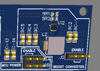
Boost converter circuit and MCU power
The boost converter is based on the MP3423, also from Microchip ( not sponsored). This circuit also performed very well in my initial test projects, with the only issue being it extremely tiny footprint, which really makes it quite difficult to use in a hobby environment, even with hot air and reflow equipment available… It is however also quite cheap, and readily available…
J5 provides enable-disable control to this part of the circuit.
With this relatively complicated power supply circuit, I thought it necessary to be able to completely isolate the ATTiny1616 and other integrated circuits from any power until I am completely sure everything works as planned…
J6A and J6B thus form a complete electrical isolation “breaker” that will prevent any voltage being provided to the microcontroller and other components on the PCB. I have doubled up on these jumpers, to allow for sufficient current flow, since I plan to use quite a few NeoPixels on this PCB… With up to 60mA of current required per pixel, that quickly adds up…
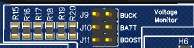
Voltage monitoring
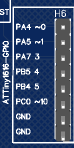
Provision was made to monitor the output voltages of the Lipo Cell, and buck and boost converters by using the analog inputs on the ATTiny1616. These can be selected by setting the jumpers on J9, J10 and J11
Alternatively, the analog inputs can be used for other applications be leaving the jumpers off, in which case these GPIO’s will be available on H6 as PA4, PA5 and PA7
The ATTiny1616 microcontroller and UPDI programming port
The heart of this PCB is the ATTiny1616 microcontroller, (microchip, not sponsored)
I decided to use the chip once again due to its low cost, as well as the fact that I do not need a very powerful processor for this application. The only issue is that requires UPDI programming. In my case, I have had no issue with that yet, but other readers did mention that they had issues with them…
The UPDI header is at H1. This header can also be used to power the processor and other integrated circuits on the PCB independently from the Power supply, like in the case where J6A and J6B are left unconnected. This use case will provide me with more testing opportunities to test the board without possible variables from the power supply circuit(s).
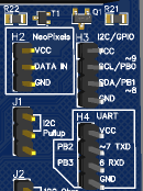
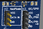
Peripherals like I2C and the UART were broken out onto headers H3 for I2C, H4 for UART. These can also be used as GPIO pins ( remember to disable the I2C pullup in J1)
CAN-Bus Support
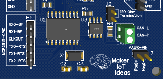
CAN-Bus support is provided by the MCP2515 (U2) and TJA1050 (U3) chips.
With access to the MCP2515 GPIO pins on H5. J2 is a 120ohm termination resistor, usually enabled at the start and end of the bus to prevent reflections.
CAN-0 is connected to the bus. An additional 12v input/output header is provided at H7
NeoPixel Header H2
The NeoPixel strips are connected to H2. They are controlled from GPIO PA6 on the ATTiny1616. I have designed around a total of 24 of these at a maximum, with a total current requirement of 1.4A ( 24 x 60mA max per pixel / 1000 = 1.44 A) .
One important fact to know about NeoPixels is that the consume about 1mA per pixel even when in the OFF state. This is due to the internal control chip requiring power to operate. While 1mA bay be a very small amount of current, a lot of them does however quickly add up, and can thus potentially drain a battery completely over time…
To prevent this from happening, I have included a PMOS switch on the VCC pin at H2. This means that no power will be fed to the Neopixel strips unless you specifically pull GPIO PC1 low.
Manufacturing the PCB
I choose PCBWay for my PCB manufacturing. Why? What makes them different from the rest?
PCBWay‘s business goal is to be the most professional PCB manufacturer for prototyping and low-volume production work in the world. With more than a decade in the business, they are committed to meeting the needs of their customers from different industries in terms of quality, delivery, cost-effectiveness and any other demanding requests. As one of the most experienced PCB manufacturers and SMT Assemblers in China, they pride themselves to be our (the Makers) best business partners, as well as good friends in every aspect of our PCB manufacturing needs. They strive to make our R&D work easy and hassle-free.
How do they do that?
PCBWay is NOT a broker. That means that they do all manufacturing and assembly themselves, cutting out all the middlemen, and saving us money.
PCBWay’s online quoting system gives a very detailed and accurate picture of all costs upfront, including components and assembly costs. This saves a lot of time and hassle.
PCBWay gives you one-on-one customer support, that answers you in 5 minutes ( from the Website chat ), or by email within a few hours ( from your personal account manager). Issues are really resolved very quickly, not that there are many anyway, but, as we are all human, it is nice to know that when a gremlin rears its head, you have someone to talk to who will do his/her best to resolve your issue as soon as possible.
This project has a lot of specific details regarding testing and assembly. Therefore I have decided to put all of that in a separate post, that you can access here.
A few months ago, I designed, what seemed at that time like an elegant solution to solve my 18650 Lipo cell charging issues. After publishing it online, I received quite a lot of extremely useful comments, most of which highlighted some of the shortcomings of that circuit.
Well, circuit is my attempt to address some of those, and turn the circuit into something that is actually useable…
What is on the PCB
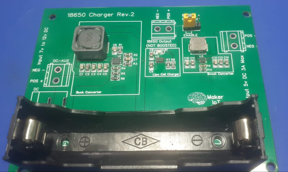
To answer this, let us start at the core and work outwards. The 18650 Lipo Cell is charged using an MCP73832T chip. This chip will charge the cell up to a nominal voltage of 4.2v DC and accept an input of up to 6.0v DC…
This presented me with my first problem, as absent-minded me accidently fried quite a few of them when accidentally connecting 12v to a PCB…
My solution to this was to add a Buck converter, based on my previous 3A Buck converter circuit(s) using the MP9943GQ from MPS. The buck converter can accept between 7v to 12v DC and output a stable 5.3v DC, saving me from frying chips, and also making it useable with most of the power supplies lying around in my lab – and it can also be used in the car at a later stage — Future project —
While that keeps the MCP73832T happy, and the 18650 cell charged, the next problem that presented itself was the nominal voltage of the 18650 cell itself, which is usually between 3.2v and 4.2v. In order for this voltage to be universally useful to me I needed a boost converter to increase the output to 5.15v.
This boost converter was built around the MP3423GG, also from MPS. This tiny little 14 pin IC provides the 5.15v that I need with ease, at a rated current of up to 3A. Ideal for powering other peripherals, like LDO regulators to power an ESP32 etc…
Manufacturing the PCB
I choose PCBWay for my PCB manufacturing. Why? What makes them different from the rest?
PCBWay‘s business goal is to be the most professional PCB manufacturer for prototyping and low-volume production work in the world. With more than a decade in the business, they are committed to meeting the needs of their customers from different industries in terms of quality, delivery, cost-effectiveness and any other demanding requests. As one of the most experienced PCB manufacturers and SMT Assemblers in China, they pride themselves to be our (the Makers) best business partners, as well as good friends in every aspect of our PCB manufacturing needs. They strive to make our R&D work easy and hassle-free.
How do they do that?
PCBWay is NOT a broker. That means that they do all manufacturing and assembly themselves, cutting out all the middlemen, and saving us money.
PCBWay’s online quoting system gives a very detailed and accurate picture of all costs upfront, including components and assembly costs. This saves a lot of time and hassle.
PCBWay gives you one-on-one customer support, that answers you in 5 minutes ( from the Website chat ), or by email within a few hours ( from your personal account manager). Issues are really resolved very quickly, not that there are many anyway, but, as we are all human, it is nice to know that when a gremlin rears its head, you have someone to talk to who will do his/her best to resolve your issue as soon as possible.
The assembly of this PCB was quite challenging, to put it lightly. 3 QFN chips, with different pad spacing, and small sizes really tested my limits. Needless to say, proper equipment is a must, and even then, a very steady hand and good magnification will go a very long way towards ensuring success… Another option would definitely be to have the PCB professionally assembled…
A stencil is definitely required for this one, is only for that 14-pin boost converter IC, to make sure that the amount of solder paste is just right – and even then, it is still a challenge!
Summary
This was a challenging build that tested my assembly skills quite a bit. The circuit functions like intended. Now it is time to add some more features, like an ideal diode chip at the output, to allow for daisy chaining the lipo cells if required, as well as maybe a microcontroller to control power to the buck converter when the battery is not being charged.
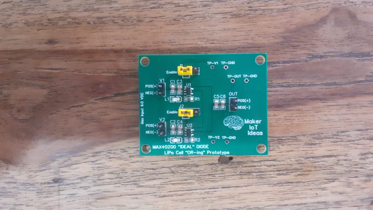
This short post will cover a quick experiment using the MAX40200 “ideal diode” chip. I have plans to incorporate this device into my Lipo Cell charger to allow for combining cells to provide longer run-time for my projects, as well as using mains power where available.
For this reason, I replicated the manufacturer evaluation circuit for the MAX40200 chip to test it under my typical operating conditions.
I include a very detailed description from EZ.Analog.com below
There are three primary applications for ideal diodes. One is simple reverse voltage protection for a battery-operated device. This is simply a diode in series from the battery to the application circuit. The second is as a diode OR for high-reliability redundant power supplies. Last is the same diode OR circuit, but for a selection circuit between an on-board rechargeable battery and a wall charger—just like your cell phone and many portable equipment have. Ideal diodes (such as the MAX16915) are also used for overvoltage protection on power inputs.
A designer could move from a standard diode to a Schottky diode in all three of the applications mentioned. That will be a big help with forward voltage drop with the voltage going from 1.1V for a standard diode to around 0.45V at a 1A forward current. But, an ideal diode will take you down to 85mV at that current, and they don’t cost much. Plus, they are much, much smaller. An ideal diode IC reduces power consumption, cuts voltage loss (important when coming from a low-voltage battery), and will take less PC board area. Besides, they solve a big Schottky problem. Schottky diodes have a very high reverse leakage—around 1mA for the 1A device. This leakage is not good for primary batteries, in particular. An ideal diode typically has a reverse leakage of less than 1µA over temperature.
There are three ways to get ideal. You could make your own, use a driver IC for an external FET, or use a device with an integrated FET. Driving the FET is not as easy as you might think. It’s important that the drive circuit control the forward voltage drop across the MOSFET to ensure smooth current transfer from one path to the other without oscillation. If the power source fails or is shorted, a fast turn-off minimizes reverse current transients. Implemented correctly, an ideal diode can provide front-end protection against reverse battery conditions, overvoltage transients, and inrush current. Ideal diode controller ICs, using external FETs, are available with current ratings up to 5A and voltage rating to 80V.
A great example of a complete ideal diode device is Maxim’s MAX40200, which operates from a supply voltage of 1.5V to 5.5V, handles up to 1A, and comes in a tiny 0.73mm square 4-bump WLP or a SOT23-5 package. It is thermally self-protecting and works over -40° to 125°C. When disabled, the MAX40200 blocks voltages up to 6V in either direction.
The functional diagram in Figure 1 shows a unique symbol for the internal FET. The p-channel FET has added circuitry to sense the MOSFET drain-to-source voltage and, in addition to driving the gate, keep the body diode reverse biased.
It should be noted that, unlike normal diodes, this “ideal diode” is not suited for rectifying AC. In applications where the supply is an inductively coupled 60Hz AC, conventional diodes should be used for the rectification part of the circuitry. MAX40200 is designed to be used in applications to switch between different DC sources. The chip exhibits a regulated ~20mV voltage drop up to 100mA of forward current. Above that, the forward drop increases to roughly 90mV at the maximum rated forward current of 1A. This small voltage drop will increase efficiency and significantly increase battery operation times. The IC’s dynamic response is detailed in an application note, “Static and Dynamic Behavior of the MAX40200 in a Diode ORing Application.” And, an evaluation kit, MAX40200EVKIT, is available.
For example, a AAA battery has 1Ah capacity at ~3V for two cells. If a Schottky diode drops 0.36V at 1A and our MAX40200 drops only 0.09V, the 0.27V difference yields 0.27Wh saved. So your device will run an extra quarter hour at the 1A maximum load.
The IC has a thermal shutdown temperature of about +154°C with 12°C hysteresis. if currents exceed ~500mA, care must be taken in your design to not exceed this temperature. The thermal performance of the WLP package actually exceeds that of the SOT package.
What is on the PCB ?
The PCB is very loosely based on the MAX40200EVKIT from MAXIM. I decided to design my own version versus buying the evaluation kit because it will , at least in my opinion, give me a better understanding of the component if I use it in a design that I have slightly modified…
What modifications did I make? Not a lot, to be honest. I added two status LED’s and enable/disable jumpers. Except for that, the circuit is stock standard from the example provided by MAXIM.
Why did I design this PCB?
The PCB was designed to thoroughly test the Diode “Or-ing” circuit, and to determine if it would function correctly when combined with my other circuits: In this case, it will be incorporated into my LiPo Cell charger in the near future.
Testing the design
I am quite happy to say that, at least to me, everything seems to be working as expected. I measured a reverse voltage of below 120mV at the input of a disabled device, and the voltage drop of an enabled device is also below about 120mV.
The OR-ing function works quite well, as well as running the two MAX40200 chips in parallel, i.e. with both enabled. This resulted in a sort of “hot-standby” configuration, where the load is powered by the highest “supply” and then almost seamlessly switched over to the other when the first supply is removed…
This functionality does however require some more testing, as I am currently unsure if it is within the recommended operating parameters of the device, as well as if the perceived “hot-swapover” is as seamless as it seems… for example, while powering a 5v LED COB light from a bench power supply at 5.3 v, there is a noticeable diming of the LED when the bench supply is removed and the circuit runs only on the 18650 Lipo cell, which is boosted to 5.15v… with a subsequent brightening of the LED once the bench supply is reactivated…
This leads me to believe that the dimming may only be due to slight voltage differences, and could thus confirm my idea that a hot swap over is actually possible.
Manufacturing the PCB
I choose PCBWay for my PCB manufacturing. Why? What makes them different from the rest?
PCBWay‘s business goal is to be the most professional PCB manufacturer for prototyping and low-volume production work in the world. With more than a decade in the business, they are committed to meeting the needs of their customers from different industries in terms of quality, delivery, cost-effectiveness and any other demanding requests. As one of the most experienced PCB manufacturers and SMT Assemblers in China, they pride themselves to be our (the Makers) best business partners, as well as good friends in every aspect of our PCB manufacturing needs. They strive to make our R&D work easy and hassle-free.
How do they do that?
PCBWay is NOT a broker. That means that they do all manufacturing and assembly themselves, cutting out all the middlemen, and saving us money.
PCBWay’s online quoting system gives a very detailed and accurate picture of all costs upfront, including components and assembly costs. This saves a lot of time and hassle.
PCBWay gives you one-on-one customer support, that answers you in 5 minutes ( from the Website chat ), or by email within a few hours ( from your personal account manager). Issues are really resolved very quickly, not that there are many anyway, but, as we are all human, it is nice to know that when a gremlin rears its head, you have someone to talk to who will do his/her best to resolve your issue as soon as possible.
Assembly is straight forward, with not difficult to-assemble components on the PCB. I did however order a stencil, as it is just part of my work-flow.
It is however completely possible to assemble this board completely by hand using a very fine tip soldering iron.
Conclusion
Using new devices – new to me, because I have not really encountered them before – can be quite exciting, especially if things turn out the way you expected, or even better than that. The challenge from this point onwards will be to properly incorporate the MAX40200 into the proposed circuit, as well as dynamically controlling each of the two MAX40200 chips to be enabled/disabled at the right time and at the right condition.
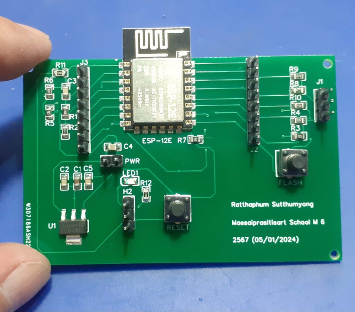
This is a student-designed ESP8266 Dev board. This project came along after I challenged some final-year students at our local high school to try to design their own PCBs. They had recently assisted me in a collaboration with the Mushroom House Controller project, and while we were talking about electronics, the idea of a challenge came up, to stimulate some interaction.
One of them was extremely confident that he could do it, providing that I gave him a schematic. I complied, and he spent the next week hacking away on the EDA software. When i saw him again, he very proudly handed me a USB flash drive, containing the EDA design, but no schematic! Oh well, let us take a chance and see what happens… I mean, how bad could it be…
I took a good look at the design, making sure that it was at least electrically sound, with all the connections made to the right components, in the right way.
That part all passed, but, as we can clearly see, the layout could be very much improved. I decided to NOT change anything on the PCB, to keep the work original.
Manufacturing the PCB
The PCB, together with a stencil, arrived from PCBWay on about the 15th of this month.
I choose PCBWay for my PCB manufacturing. Why? What makes them different from the rest?
PCBWay‘s business goal is to be the most professional PCB manufacturer for prototyping and low-volume production work in the world. With more than a decade in the business, they are committed to meeting the needs of their customers from different industries in terms of quality, delivery, cost-effectiveness and any other demanding requests. As one of the most experienced PCB manufacturers and SMT Assemblers in China, they pride themselves to be our (the Makers) best business partners, as well as good friends in every aspect of our PCB manufacturing needs. They strive to make our R&D work easy and hassle-free.
How do they do that?
PCBWay is NOT a broker. That means that they do all manufacturing and assembly themselves, cutting out all the middlemen, and saving us money.
PCBWay’s online quoting system gives a very detailed and accurate picture of all costs upfront, including components and assembly costs. This saves a lot of time and hassle.
PCBWay gives you one-on-one customer support, that answers you in 5 minutes ( from the Website chat ), or by email within a few hours ( from your personal account manager). Issues are really resolved very quickly, not that there are many anyway, but, as we are all human, it is nice to know that when a gremlin rears its head, you have someone to talk to who will do his/her best to resolve your issue as soon as possible.
Technically, this PCB does not actually need it, as the components are large enough to manually place solder paste. This being a student project, I did however choose to get the stencil to try and assure the best possible chance of success..
Placing components only took a few minutes, after which the PCB was reflowed with hot air – no need for a hotplate here!
Through-hole components took only another few minutes to solder into place, and then testing could commence.
My thoughts – a very “gentle” critique
The board could be smaller, but due to the fact that this is a “very first PCB ever” and also a first SMD PCB at that, I can understand that it may still be quite difficult to understand how small the components really are, as well as lay them out properly.
Components are mostly all over the board, without a clear “group by function” kind of mindset. This once again comes back to experience.
GPIO pins are not notated. This will really make the board difficult to use. The power supply input is in the center of the PCB. This is definitely not ideal.
In general, track sizes could have been bigger, especially on the Power and Ground lines. No ground plane was poured on either layer.
So does it work? Yes, surprisingly it does. We shall see more of it in the near future, when I task the creator with using it to perform some task. That way, he can experience first hand the difficulties of the design, and also learn practically why certain things need to be improved.
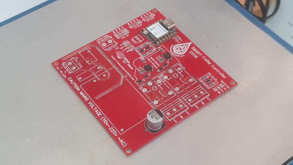
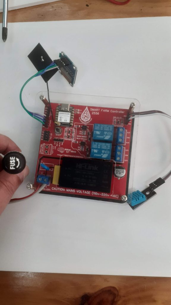
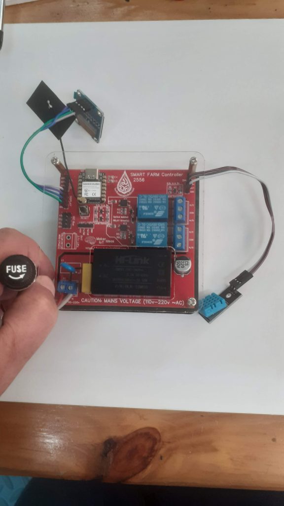
This is a Simple IoT Plant Watering Solution, done as another collaboration with the local High School in my Area. In this project, they took a group of purely academic students ( Language majors ) and told them that they had to design an electronics project that would have use in the real world…
This presented a very tough situation to the students since they had never even imagined that they could do something like this… (Think along the lines of a Senior Design project, like what you would give EE Students during their final year – with all the documentation, pamphlets, and explanations – i.e. lots and lots of paperwork) , and then also add on the requirement that they had to present a practical project as well! And they have only 45 days to do that as well!
I came into this picture late on a Thursday or Friday afternoon, with a group of students milling around outside the Electronics lab. They were unknown to me and seemed quite flustered… I invited them in, and eventually, they started opening up about their problem…
As it turned out, they were completely clueless, and did not know where to start with anything, not even what they wanted to do! Their initial idea went like “something that uses a camera to sort garbage by type and material” – that was never going to happen, not in 45 days, and not with the allocated budget of no more than $USD30.00 they were allowed. Lets not even go to the machine learning stuff, training of the models etc…
So, I took over, and decided that we shall do a simple IoT Plant Watering Solution. It is complex enough for Grade 11 students, and more importantly, I knew that I could teach them enough Arduino coding and basic electronics skills in the time allotted to get the project completed successfully.
What followed was a few very intensive sessions after school to get the paperwork sorted. For some reason, their teacher required ALL paperwork be completed upfront, with the entire design and code prepared before they touched the practical stuff – A funny way to design stuff if you ask me, but that is how we did it…
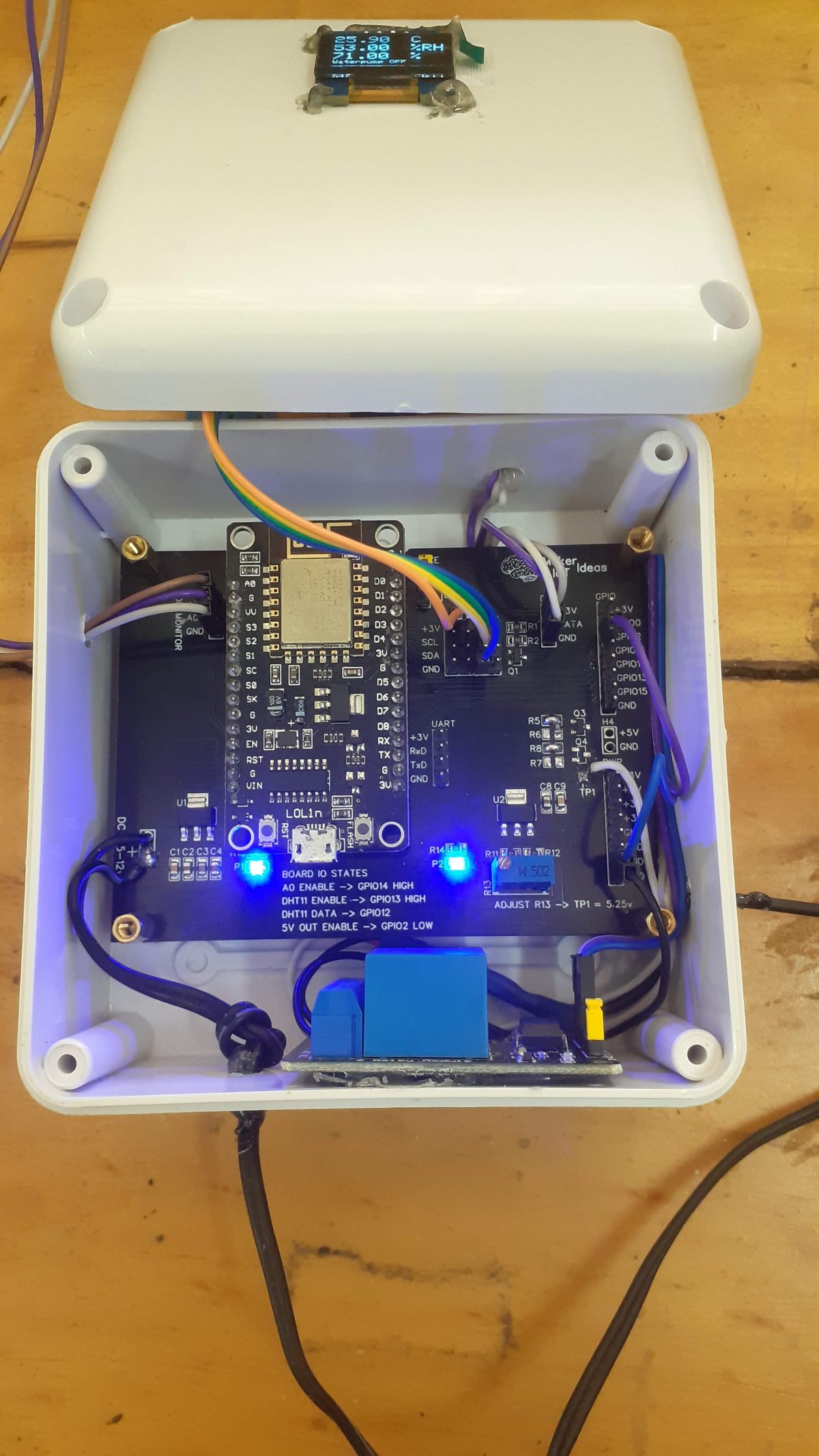
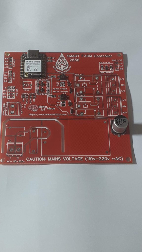
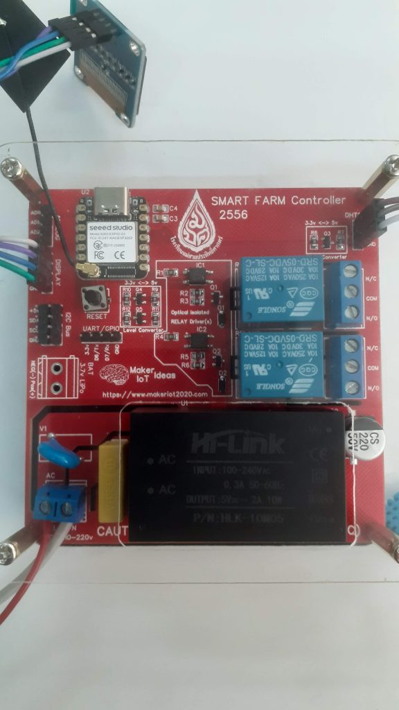
We settled on the ESP8266 12-E NodeMCU v3 development board, A resistive soil sensor, a DHT11 for temperature and humidity data, a small OLED I2C display and a small 5v USB-powered water pump. While they ordered the components, we started with basic coding classes, and this is where the story changes.
These kids blew me away with their level of interest, their attitude to learning, and how quickly they grasped the concepts. In no time at all, they were coding basic sketches, taking readings, learning how the different sensors worked, and pushing the envelope by adding lots more complementary components like MOSFETs and BJT transistors.
With this level of enthusiasm, I could not help but also become very excited, and thus decided to go a bit further than usual and help them design a neat PCB baseboard for the NodeMCU. That way, we could get rid of all those pesky wire connections, and maybe even produce something that looked good.
This is what we came up with, here shown just after SMD component placing. They ( the students ) did all of that by themselves as well, and it turned out to be a lot of fun for them, with some funny moments for me as well.
The Assembly ( First time ever )
The PCB, together with a stencil, arrived from PCBWay on about the 15th of this month.
I choose PCBWay for my PCB manufacturing. Why? What makes them different from the rest?
PCBWay‘s business goal is to be the most professional PCB manufacturer for prototyping and low-volume production work in the world. With more than a decade in the business, they are committed to meeting the needs of their customers from different industries in terms of quality, delivery, cost-effectiveness and any other demanding requests. As one of the most experienced PCB manufacturers and SMT Assemblers in China, they pride themselves to be our (the Makers) best business partners, as well as good friends in every aspect of our PCB manufacturing needs. They strive to make our R&D work easy and hassle-free.
How do they do that?
PCBWay is NOT a broker. That means that they do all manufacturing and assembly themselves, cutting out all the middlemen, and saving us money.
PCBWay’s online quoting system gives a very detailed and accurate picture of all costs upfront, including components and assembly costs. This saves a lot of time and hassle.
PCBWay gives you one-on-one customer support, that answers you in 5 minutes ( from the Website chat ), or by email within a few hours ( from your personal account manager). Issues are really resolved very quickly, not that there are many anyway, but, as we are all human, it is nice to know that when a gremlin rears its head, you have someone to talk to who will do his/her best to resolve your issue as soon as possible.
This caused quite a lot of excitement from the students since they asked me to get to school immediately, and offered to stay after school to get the assembly done. So, I packed up all the components required, got in the car, and a few minutes later, we had an assembly line running 🙂
It took them only a few minutes to understand how to read the BOM file, use that information to find the right components and take turns to place a few components at a time onto the PCB. ( I did the solder paste and stencil thing on my own, as that could potentially turn out to be a very messy and wasteful operation if I let them do it )
During this assembly, they were quite amazed at what they were doing, but also quite confused as to how we would ” make the components stick to the PCB later”. They have seen soldering on YouTube, and could not understand how this “grey paste” could “turn hard and shiny” – with some even trying to rush their friends, as the paste would dry up and become sticky…
That signalled to me that we should get the hot air ready, and show them properly, as it would stop the speculation, and give them closure on their questions, because no matter how much I tried to explain that the solder paste would be melted later, they could not understand that concept.
Once I reflowed the first few components using hot air, they all once again took turns with a small group of components on the PCB ( We assembled 2 PCB’s to make sure everybody got a chance to try everything)
Through-hole soldering of the various header pins and other components was next. Once again, I showed them an example and then stepped back while they took over and completed the task. At this time it was about 17:30 already, so I sent them all home, with a promise to return the next day and complete the rest of the build.
Final Assembly and the Enclosure
We added some copper standoffs to the bottom of the enclosure, drilled some holes and mounted everything with screws and hot glue. The some final testing was performed, and the project was placed outside, next to a potted plant, and put on a sort of soak test, to verify operation for a few days.
A discussion of the circuit
In this circuit, I made use of a very cheap resistive soil moisture probe sensor. It consists of an etched PCB probe and a separate OPAMP on an additional PCB. This assembly then sends an analog voltage back to the Microprocessor for analysis. Very easy to use, and as mentioned, extremely cheap! But this is also a big problem. As seen in many other posts online, people don’t like these probes, as they don’t seem to last very long, and/or become unreliable over time.
I believe that this is due to the fact that they run them continuously, and that, causes the electrodes to erode away over time – because the thing about it, you are basically running an electrolysis cell – sending voltage/current through a probe, that is suspended in a conductive medium ( the water in the soil contains minerals etc – that is why it is conductive, and why we can get a reading from it )
How do I plan to avoid this problem then? The probe is powered through a small N-Channel MOSFET. This allows us to power the probe on when we want a reading, and then power it off again. It will definitely not completely stop the electrodes eroding away over time, but I am sure it will extend the usable lifetime of the probe by quite a bit. On the downside, you need another GPIO pin to control that MOSFET, but that in itself is also a great learning opportunity
This project was extremely interesting. It was something very basic, but it gave me a very unique opportunity to teach a group of kids something they never knew before. It also initiated a spark in many of them, who are now interested in getting involved in electronics as a hobby. The possibilities of this project, if it is improved a bit more, could also be great. For example, we did not even consider adding IoT connectivity to this yet, we all decided that it was not needed, and an unnecessary complication of an already complex issue ( to the students that is). I shall keep monitoring the operation of the device over the next few weeks, and hopefully get some answers myself as to how long that soil probe will last… As a control, we have another one that was left powered on in the same container. That one are not being used to take readings, but will definitely provide us with a good comparison against the probe that is only on then used…
Over the last few months, We have been steadily improving the design of our XIAO RP2040-based mouse device. With this, ver 3.0 all the hardware bugs were finally eliminated, and we also placed the device into its first-ever enclosure.
Let us take a look at the design
The PCB and Schematic
The PCB is a very strange shape, with lots of cut-outs. This is to accommodate the big push buttons that will be mounted in the enclosure, as well as to fit nicely into the mounting area of the enclosure… This design took quite some time with a pair of callipers and CAD, but all went well, and the shape is perfectly accurate.
The schematic is also straight forward, with the only real changes begin to the rotary encoder. In ver 2.0, We connected the encoder to the MCP23008, but for some reason CircuitPython does not seem to like an encoder connected to an IO extender… That forced us to do some software hack to use the encoder… I have thus decided to change things around in ver 3.0 and move the encoder back to the native GPIO on the XIAO RP2040
It is also interesting to note that the circuit was initially designed for the XIAO ESP32S3, but due to issues with stock, as well as crazy prices on local parts, we made a quick turn-around and went back to the RP2040. The ESP32S3 was going to allow us to implement a wireless device, through using ESPNow protocol… That may still be done in future, but for now, I think we have done enough work on the mouse device for the time being…
Manufacturing the PCB and Assembly
I choose PCBWay for my PCB manufacturing. Why? What makes them different from the rest?
PCBWay‘s business goal is to be the most professional PCB manufacturer for prototyping and low-volume production work in the world. With more than a decade in the business, they are committed to meeting the needs of their customers from different industries in terms of quality, delivery, cost-effectiveness and any other demanding requests. As one of the most experienced PCB manufacturers and SMT Assemblers in China, they pride themselves to be our (the Makers) best business partners, as well as good friends in every aspect of our PCB manufacturing needs. They strive to make our R&D work easy and hassle-free.
How do they do that?
PCBWay is NOT a broker. That means that they do all manufacturing and assembly themselves, cutting out all the middlemen, and saving us money.
PCBWay’s online quoting system gives a very detailed and accurate picture of all costs upfront, including components and assembly costs. This saves a lot of time and hassle.
PCBWay gives you one-on-one customer support, that answers you in 5 minutes ( from the Website chat ), or by email within a few hours ( from your personal account manager). Issues are really resolved very quickly, not that there are many anyway, but, as we are all human, it is nice to know that when a gremlin rears its head, you have someone to talk to who will do his/her best to resolve your issue as soon as possible.
Assembly was quite easy, I chose to use a stencil, because the IO Expander chip has a very tiny footprint, as well as a leadless package… The stencil definitely helps prevent excessive solder paste, as well as saves a lot of time on reworking later…
In the picture above, we can clearly see why I had to design the PCB with such an irregular shape.
Firmware and Coding
We are still using CircuitPython for the firmware on this device. It is not perfect, but it works, well sort of anyway. What does that mean? Well… As far as the mouse functions are concerned, clicking, scrolling, moving the pointer – all of that is works perfectly, and thus allows me to use the device for basic operations every day. Drag and Drop, as well as selecting and or highlighting text DOES NOT work. This seem to be an issue with the HID code in Circuitpython, meaning it doesn’t seem to be implemented. It is also way beyond my abilities to implement it myself…
Below is the code.py file, with the boot.py below that
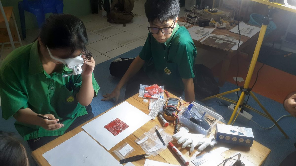
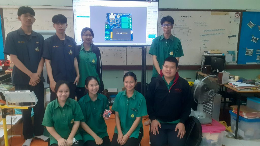
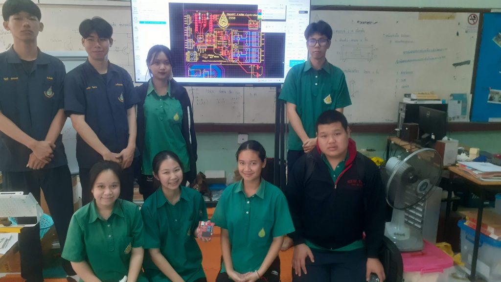
A Collaboration with Maesai Prasisart School, Measai, Chiang Rai, Thailand
In part two of the project, we let the students assemble the Mushroom house controller that they helped to design. It is important to note that they have never done any of this before, and also that most of the components are SMD.
This made for some interesting moments…
The PCB Arrives
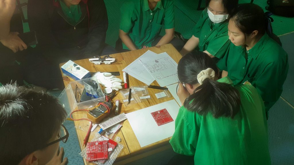
The PCB arrived from the factory, and after an initial inspection by myself, we took it to the school so that a specially selected group of students can try their hand at assembling it.
One of the first remarks by the students was that everything was so tiny… Having never seen SMD assembly, they wrongly assumed that they would be required to manually solder the components using traditional solder and a soldering iron… This feeling of “dismay” was greatly increased when we started laying out the small bags with components.
I choose PCBWay for my PCB manufacturing. Why? What makes them different from the rest?
PCBWay‘s business goal is to be the most professional PCB manufacturer for prototyping and low-volume production work in the world. With more than a decade in the business, they are committed to meeting the needs of their customers from different industries in terms of quality, delivery, cost-effectiveness and any other demanding requests. As one of the most experienced PCB manufacturers and SMT Assemblers in China, they pride themselves to be our (the Makers) best business partners, as well as good friends in every aspect of our PCB manufacturing needs. They strive to make our R&D work easy and hassle-free.
How do they do that?
PCBWay is NOT a broker. That means that they do all manufacturing and assembly themselves, cutting out all the middlemen, and saving us money.
PCBWay’s online quoting system gives a very detailed and accurate picture of all costs upfront, including components and assembly costs. This saves a lot of time and hassle.
PCBWay gives you one-on-one customer support, that answers you in 5 minutes ( from the Website chat ), or by email within a few hours ( from your personal account manager). Issues are really resolved very quickly, not that there are many anyway, but, as we are all human, it is nice to know that when a gremlin rears its head, you have someone to talk to who will do his/her best to resolve your issue as soon as possible.
To make things easier for them, I had previously selected all components, and together with a label and component designators, placed each component into a separate anti-static plastic bag. This achieved two things – it shielded the students from having to handle reels of components, potentially resulting in a lot of wastage, and it make it almost impossible to place a wrong component in a wrong place, as each of the bags were clearly marked with the specific component designator of the component it contained.
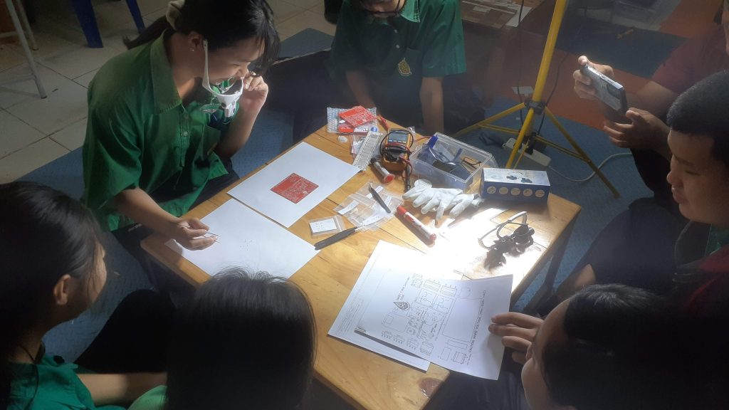
Their feelings of “dismay” were quickly replaced with wonder as I used a stencil to apply solder paste to the PCB. There were also confusing present, as they could not understand how the “sticky” solder would melt and keep the component in place. They were also quite worried about placing the components onto the PCB – that was until they saw that there was a selection of fine tweezers set out to use for exactly this purpose…
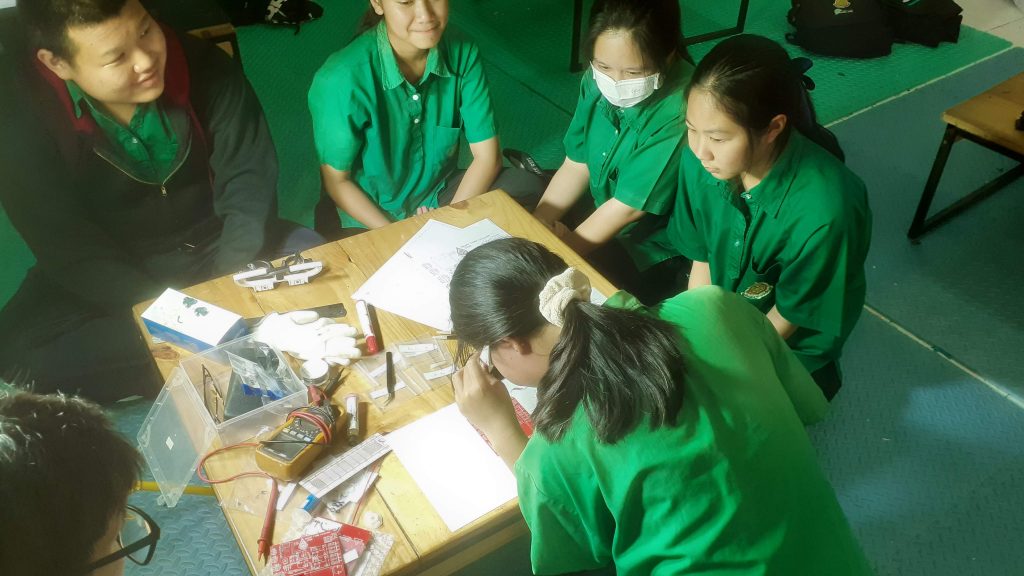
They now became very excited and took turns to each place a few components onto the PCB. I took special care to keep the diodes, optic isolators and microcontroller well away from them, at least until I explained that these components were polarised, or had to be placed in a specific orientation onto the board.
After a bit of struggling with the diodes, as well as the microcontroller, all the SMD components were eventually correctly placed onto the PCB. I now took over and used a hotplate to reflow the PCB.
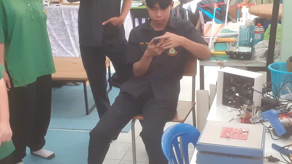
This process completely amazed them, or at least, most of them, as some took this opportunity to continue with the ever present interaction of students and mobile phones that are so common in SE Asia 🙂
The PCB was now reflowed, and after a short break to let things cool down, we continued with the soldering and assembly of the through-hole components.
The proceedings would not be complete without a group photo of the students and the PCB that they assembled.
Conclusion of part 2
With the PCB now assembled, I used my desktop CNC machine to cut acrylic plastic to form a protective shell. The PCB will soon be installed at the remote site shown in part 1, and while it will be inside a IP65 electrical enclosure, I still felt the need for a little bit of added protection.
The firmware development is complete, and we are currently busy bringing the students up to date with the exact operation thereof. Our goal is that they would at least try to create their own version of the firmware for use in the electronics lab, as well as a comparison between my version of the firmware and theirs.
From the smiles on their faces during the entire process, it was quite obvious that they really enjoyed this project.
A Collaboration with Maesai Prasisart School, Maesai, Chiang Rai, Thailand
A short while ago, the local high school in my area and myself decided to collaborate on a real-world project regarding an IoT device. The device (prototype above) will be used as a controller in an Oyster Mushroom growing house, which in turn will be managed by the members of a local disabled persons association. This is very exciting for a few reasons…
I will get the opportunity to teach interested students how to solve real-world problems using electronics, as well we will do something for the community and thus contribute to making the lives of the local disabled people a bit easier.
In the long term, the data collected by the device can be used to teach other mushroom growers in the area about the optimum environment to help them ensure that they get the perfect harvest every time…
In this post, I will thus do things a little differently from my normal setup, and focus more on the collaboration, as well as teaching moments. I shall also include quite a lot of pictures. The usual schematics and PCB descriptions shall still be available, but only on the PCBWay Shared projects page ( link to be added in due course)
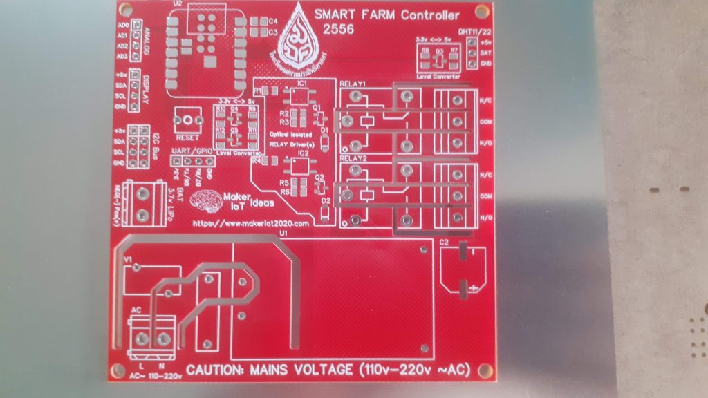
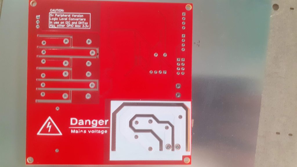
The initial idea is to produce two different PCB’s with basically the same function, for the time being designed by myself. One, used in this post, will be a 3.3v version, with battery backup, and the other will be a 5v version, with level converters ( I could not resist the potential teaching opportunity that these provided) and no battery backup. The 5v version, which I shall introduce in part 2 will be assembled by the students, while I shall assemble the 3.3v version.
Further to that, the goal is to break the PCB up into logical modules and teach the students about each module. Their task would be to then design a PCB of that module, and in the end, combine all the modules into a functional project. As a further part to this, a special interest group shall then make use of the knowledge learnt during the development of the modules to design a third PCB including all of those modules, as well as any other that they find may be needed, assemble it and use it in the real world.
Gallery – At the remote site
Over here, Grade 12 students assist in the construction of a mushroom house. The pictures do not need a lot of captions, as they are quite self-explanatory
The next day, in the classroom
We started with a prototype on a breadboard, with some basic firmware. This was followed by a simple PCB design (with frequent 3D views so that the students could see what was happening)
This was followed by a practical session where the students had the opportunity to try their hand at designing a part of the PCB. It is quite important that we understand that this is the very very first time in their lives that they were ever exposed to this. They were all extremely excited and some grasped the concepts quite fast, while others took a more cautious approach…
Manufacturing the PCB
Now it was up to me to finalise the initial design and get it manufactured.
I choose PCBWay for my PCB manufacturing. Why? What makes them different from the rest?
PCBWay‘s business goal is to be the most professional PCB manufacturer for prototyping and low-volume production work in the world. With more than a decade in the business, they are committed to meeting the needs of their customers from different industries in terms of quality, delivery, cost-effectiveness and any other demanding requests. As one of the most experienced PCB manufacturers and SMT Assemblers in China, they pride themselves to be our (the Makers) best business partners, as well as good friends in every aspect of our PCB manufacturing needs. They strive to make our R&D work easy and hassle-free.
How do they do that?
PCBWay is NOT a broker. That means that they do all manufacturing and assembly themselves, cutting out all the middlemen, and saving us money.
PCBWay’s online quoting system gives a very detailed and accurate picture of all costs upfront, including components and assembly costs. This saves a lot of time and hassle.
PCBWay gives you one-on-one customer support, that answers you in 5 minutes ( from the Website chat ), or by email within a few hours ( from your personal account manager). Issues are really resolved very quickly, not that there are many anyway, but, as we are all human, it is nice to know that when a gremlin rears its head, you have someone to talk to who will do his/her best to resolve your issue as soon as possible.
The assembly of the first board was done by myself, and firmware development was started. Stay tuned for Part 2 where the students will get the opportunity to assemble a SMD PCB for the very first time in their lives…
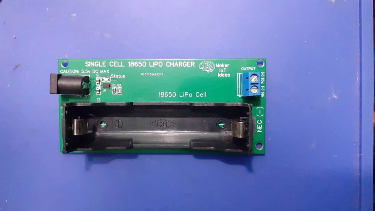
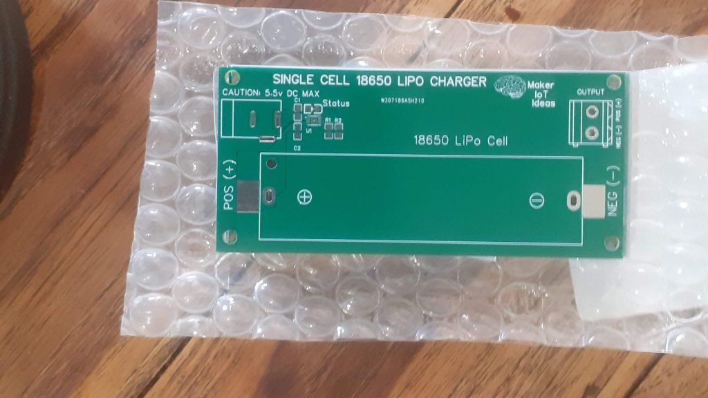
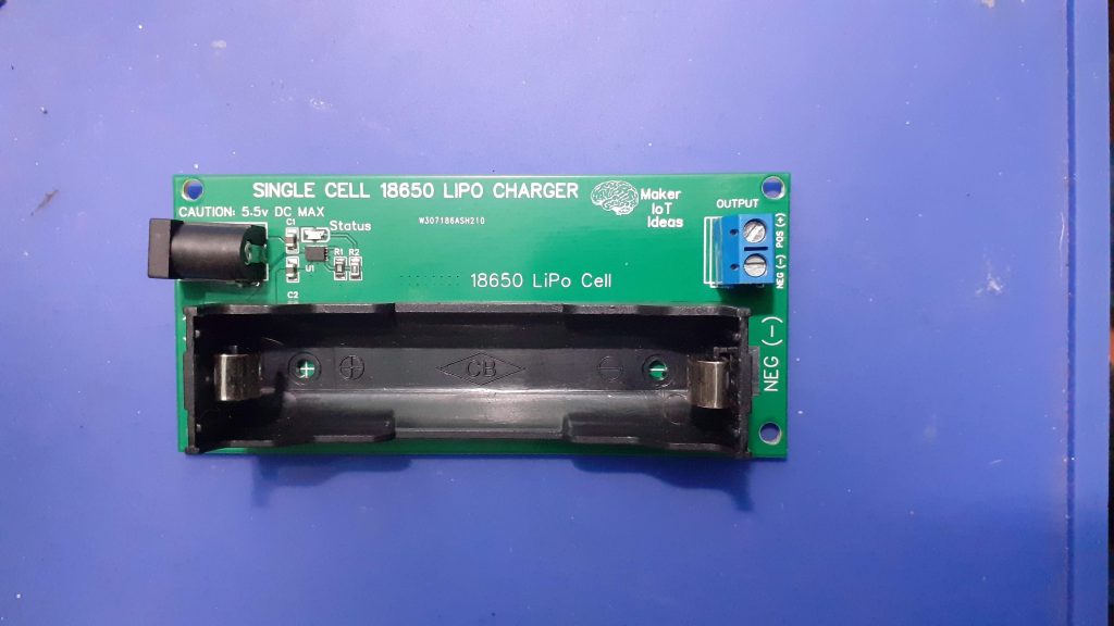
This single cell lipo charger was created to solve a problem I encountered during a recent project. I constantly needed to recharge 18650 cells, and while I could also use my 4-cell charger, that didn’t always turn out to be the most practical. I also intend to use this small charger as a building block for a future complete power solution, including a boost converter, more protection features and proper cell status indication…
I am currently moving towards building more projects that will be used outside, “in the wild” and thus need a reliable way to power those. True to my way of doing things, I want to build my own stuff as far as possible. That way, I learn more about the technology, and I am sure that everything meets my exact specifications.
What is on the PCB?
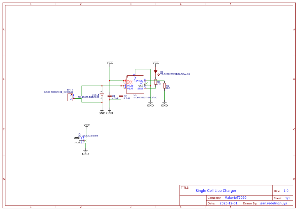
The charger is based on the MCP73832T, by Microchip, which contains quite a lot of useful features, in a small package as well at a relatively small price tag, and with very few other required supporting components.
Linear Charge Management Controller:
Integrated Pass Transistor
Integrated Current Sense
Reverse Discharge Protection
High Accuracy Preset Voltage Regulation: + 0.75%
Four Voltage Regulation Options:
4.20V, 4.35V, 4.40V, 4.50V
Programmable Charge Current: 15 mA to 500 mA
Selectable Preconditioning:
10%, 20%, 40%, or Disable
Selectable End-of-Charge Control:
5%, 7.5%, 10%, or 20%
Charge Status Output
Tri-State Output – MCP73831
Open-Drain Output – MCP73832
Automatic Power-Down
Thermal Regulation
Temperature Range: -40°C to +85°C
Packaging:
8-Lead, 2 mm x 3 mm DFN
5-Lead, SOT-23
A proper screw-type connection terminal on the output, as well as a DC Barrel Jack on the input, completes the PCB. On future revisions, I will seriously consider having a voltage-limiting circuit on the input side, since the MCP73832T is only capable of accepting an input voltage of up to 5.5v DC.
This is not a problem to me, as I will be using the current version for my own personal use. I do however believe it is essential to ensure that no over-voltage conditions can accidently occur BEFORE I will give this to someone else to use.
The schematic
Manufacturing the PCB
I choose PCBWay for my PCB manufacturing. Why? What makes them different from the rest?
PCBWay‘s business goal is to be the most professional PCB manufacturer for prototyping and low-volume production work in the world. With more than a decade in the business, they are committed to meeting the needs of their customers from different industries in terms of quality, delivery, cost-effectiveness and any other demanding requests. As one of the most experienced PCB manufacturers and SMT Assemblers in China, they pride themselves to be our (the Makers) best business partners, as well as good friends in every aspect of our PCB manufacturing needs. They strive to make our R&D work easy and hassle-free.
How do they do that?
PCBWay is NOT a broker. That means that they do all manufacturing and assembly themselves, cutting out all the middlemen, and saving us money.
PCBWay’s online quoting system gives a very detailed and accurate picture of all costs upfront, including components and assembly costs. This saves a lot of time and hassle.
PCBWay gives you one-on-one customer support, that answers you in 5 minutes ( from the Website chat ), or by email within a few hours ( from your personal account manager). Issues are really resolved very quickly, not that there are many anyway, but, as we are all human, it is nice to know that when a gremlin rears its head, you have someone to talk to who will do his/her best to resolve your issue as soon as possible.
Assembly of this PCB was quite easy, providing that you have a stencil, it will not take you more than a few minutes.
The PCB’s really came out very nicely 🙂
I have also made provision for using a through-hole 18650 battery holder, just in case you are like me, and have a few lying around in a drawer, or could just not be bothered with using the SMD version…
The completed PCB is relatively small and compact, taking into consideration the size of the 18650 cell of course… The screw terminal on the output really helps to keep everything secure when using the module to power a project, and the DC barrel jack provides a good connection to charge it all back up again… Now, If I just remembered to add some form of voltage limiting on the input, as well as include a boost converter, It would be the perfect little “power bank” project… For now though, let’s leave those features to the future, as this is already extremely useful as is.