A Collaboration with Maesai Prasisart School, Measai, Chiang Rai, Thailand
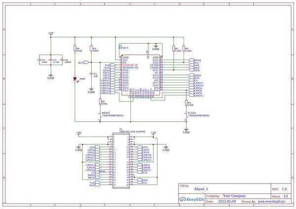
In part two of the project, we let the students assemble the Mushroom house controller that they helped to design. It is important to note that they have never done any of this before, and also that most of the components are SMD.
This made for some interesting moments…
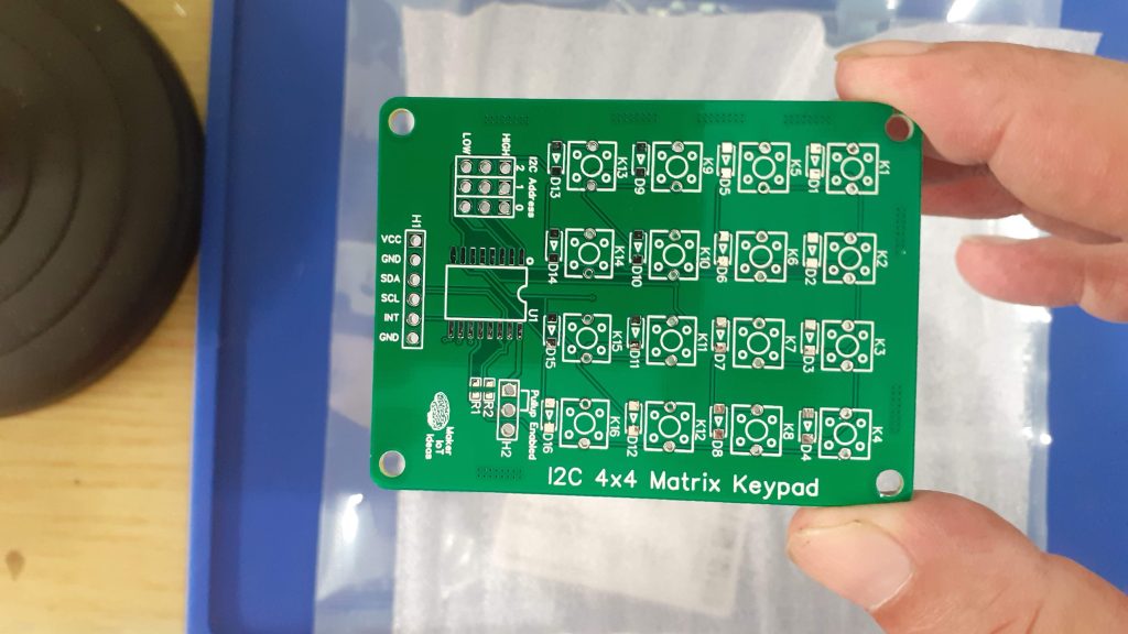
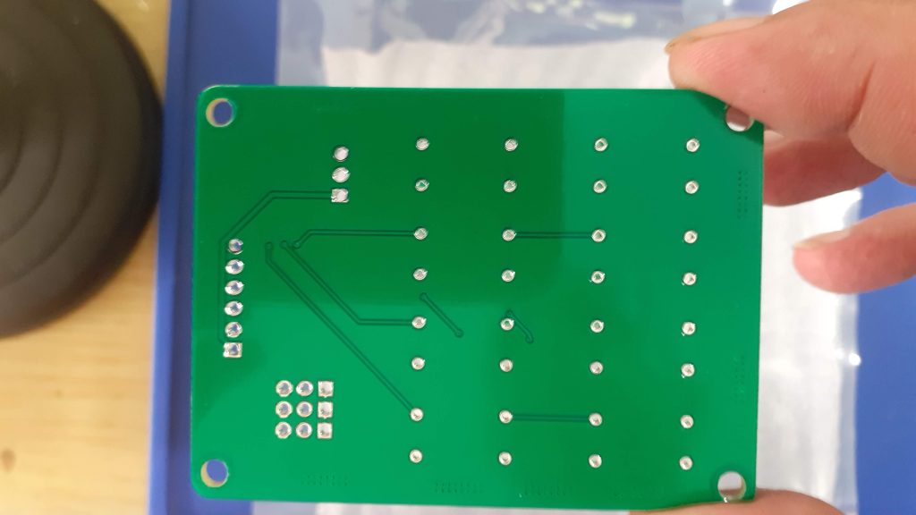
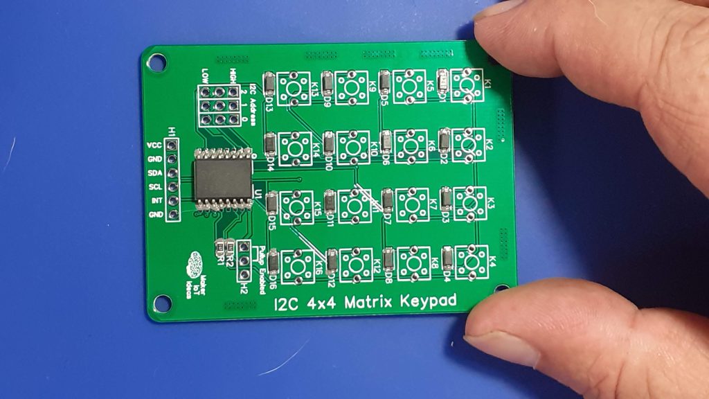
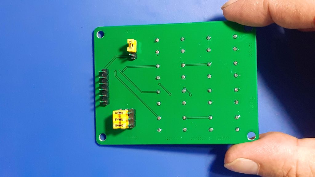
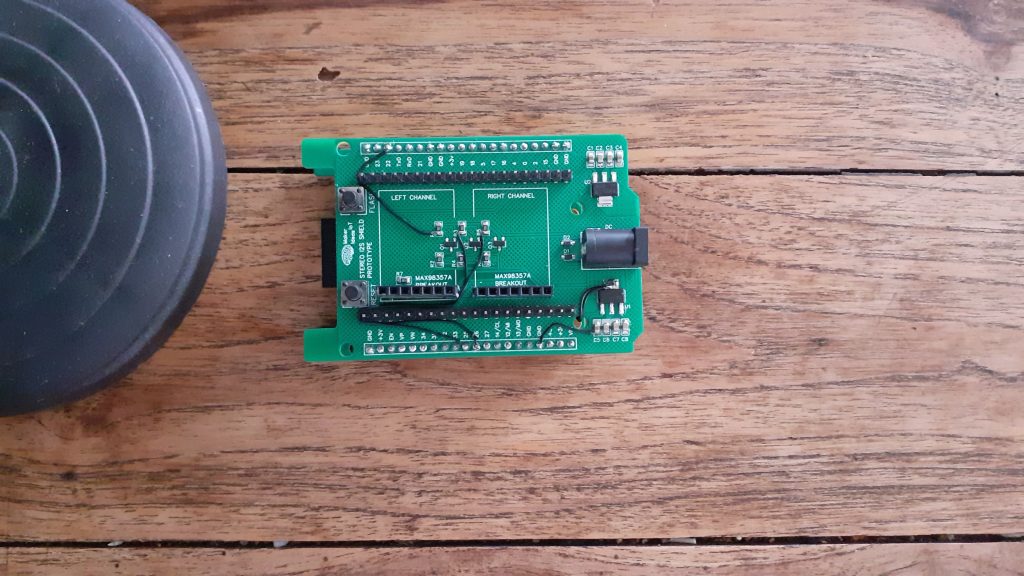
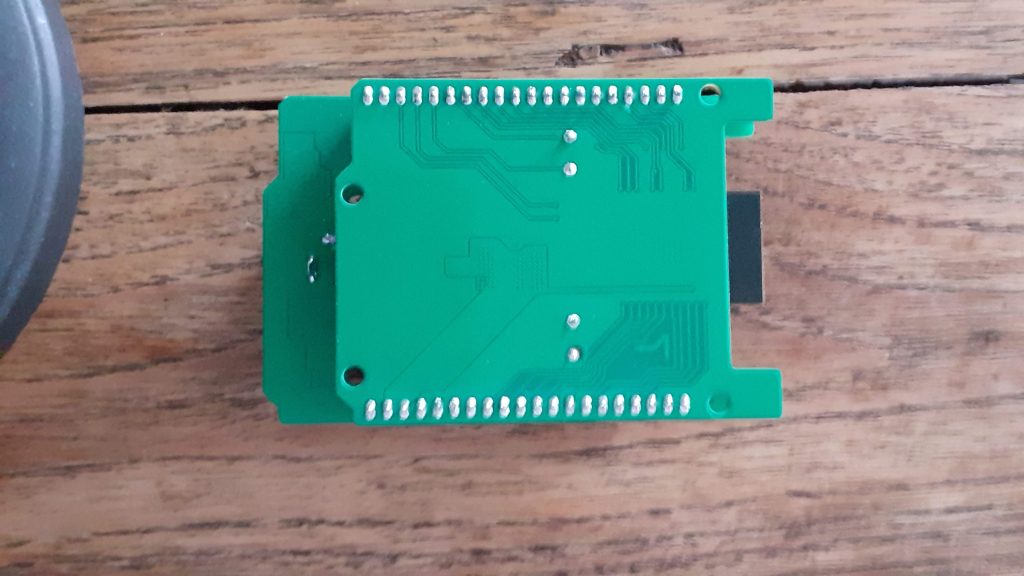
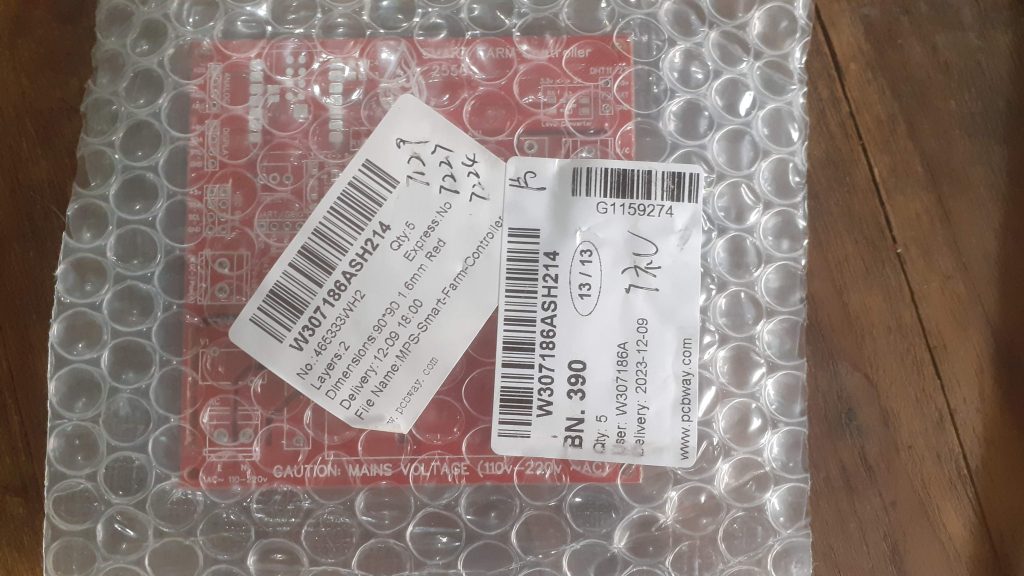
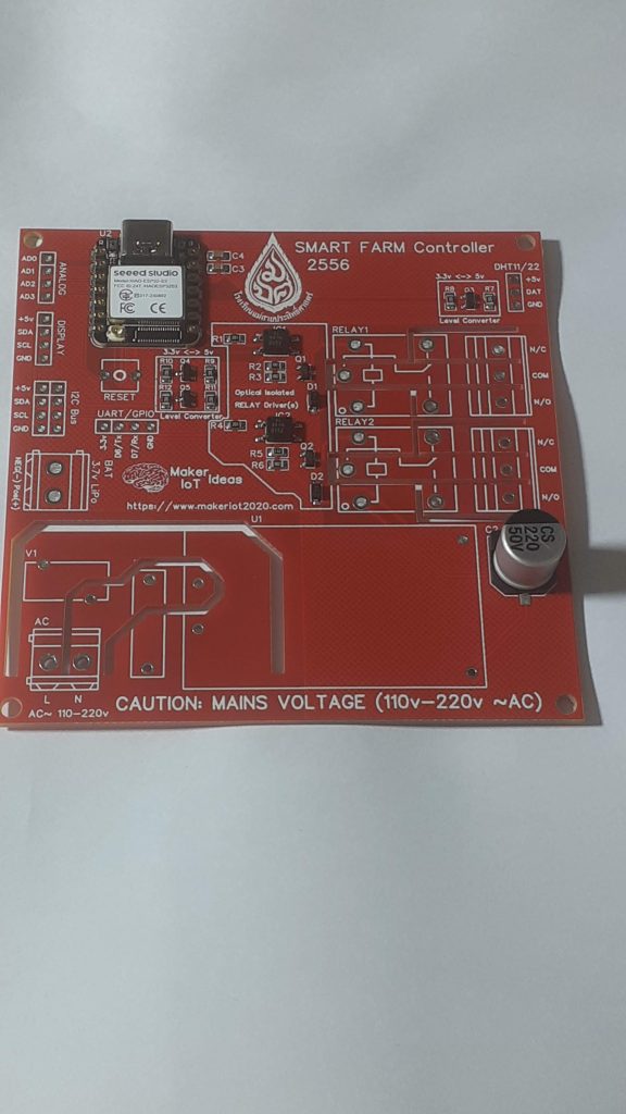
The PCB Arrives
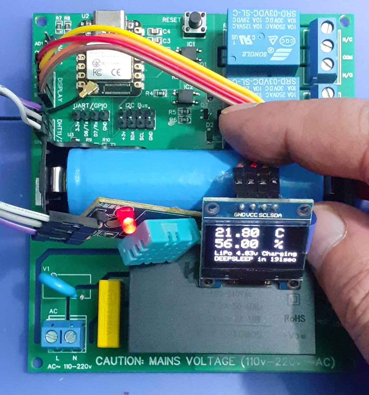
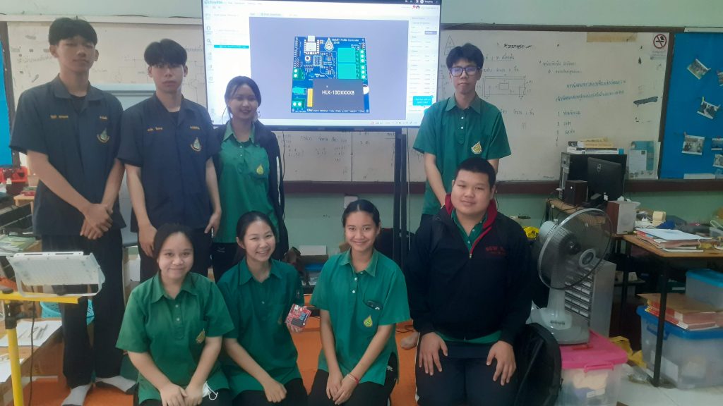
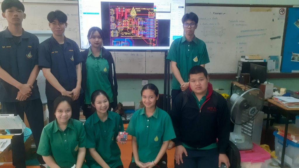
The PCB arrived from the factory, and after an initial inspection by myself, we took it to the school so that a specially selected group of students can try their hand at assembling it.
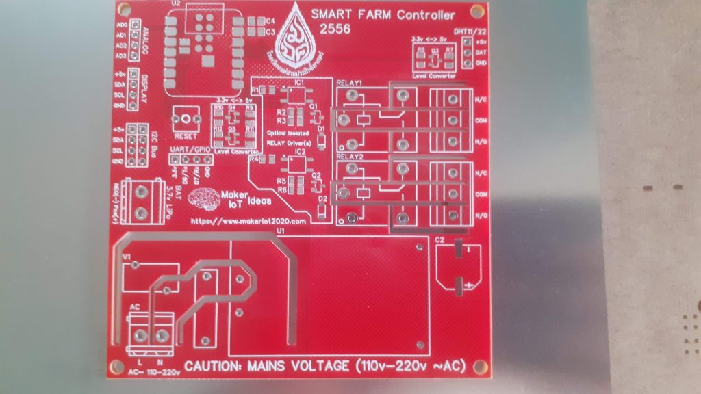
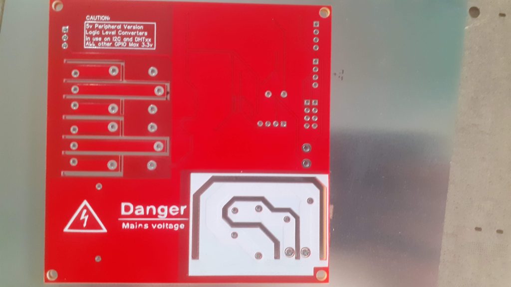
One of the first remarks by the students was that everything was so tiny… Having never seen SMD assembly, they wrongly assumed that they would be required to manually solder the components using traditional solder and a soldering iron… This feeling of “dismay” was greatly increased when we started laying out the small bags with components.
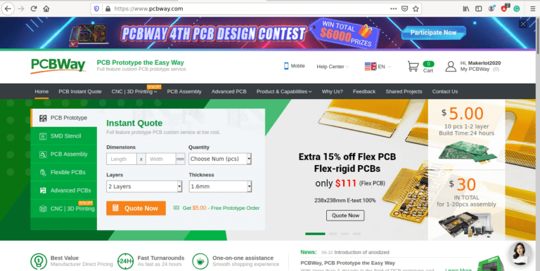
I choose PCBWay for my PCB manufacturing. Why? What makes them different from the rest?
PCBWay‘s business goal is to be the most professional PCB manufacturer for prototyping and low-volume production work in the world. With more than a decade in the business, they are committed to meeting the needs of their customers from different industries in terms of quality, delivery, cost-effectiveness and any other demanding requests. As one of the most experienced PCB manufacturers and SMT Assemblers in China, they pride themselves to be our (the Makers) best business partners, as well as good friends in every aspect of our PCB manufacturing needs. They strive to make our R&D work easy and hassle-free.
How do they do that?
PCBWay is NOT a broker. That means that they do all manufacturing and assembly themselves, cutting out all the middlemen, and saving us money.
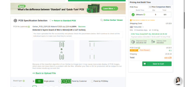
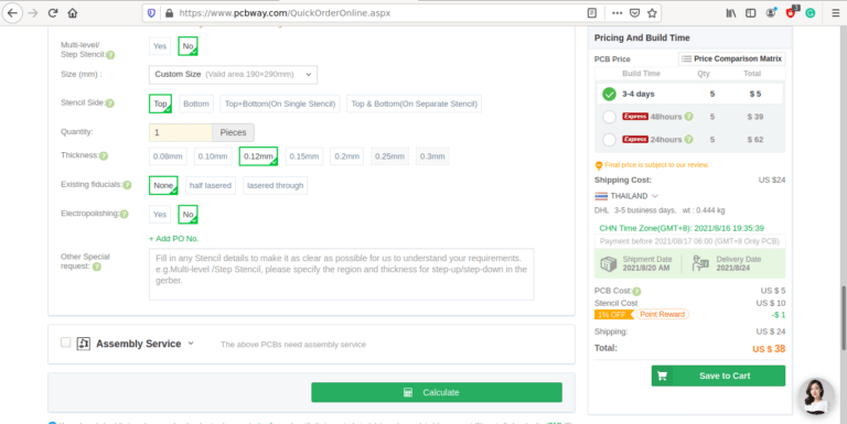
PCBWay’s online quoting system gives a very detailed and accurate picture of all costs upfront, including components and assembly costs. This saves a lot of time and hassle.
PCBWay gives you one-on-one customer support, that answers you in 5 minutes ( from the Website chat ), or by email within a few hours ( from your personal account manager). Issues are really resolved very quickly, not that there are many anyway, but, as we are all human, it is nice to know that when a gremlin rears its head, you have someone to talk to who will do his/her best to resolve your issue as soon as possible.
Find out more here


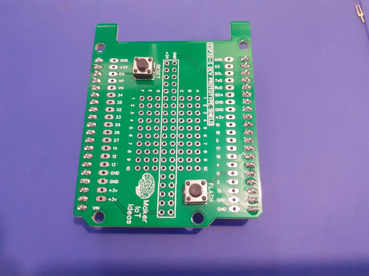
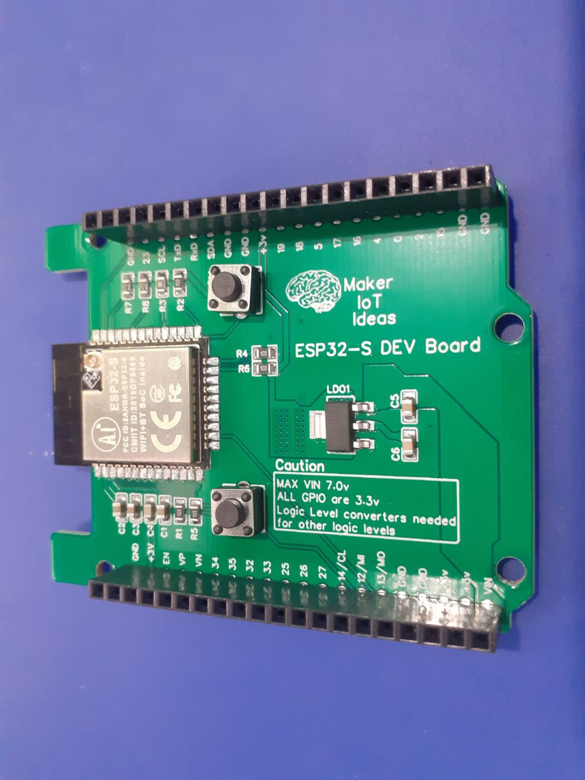
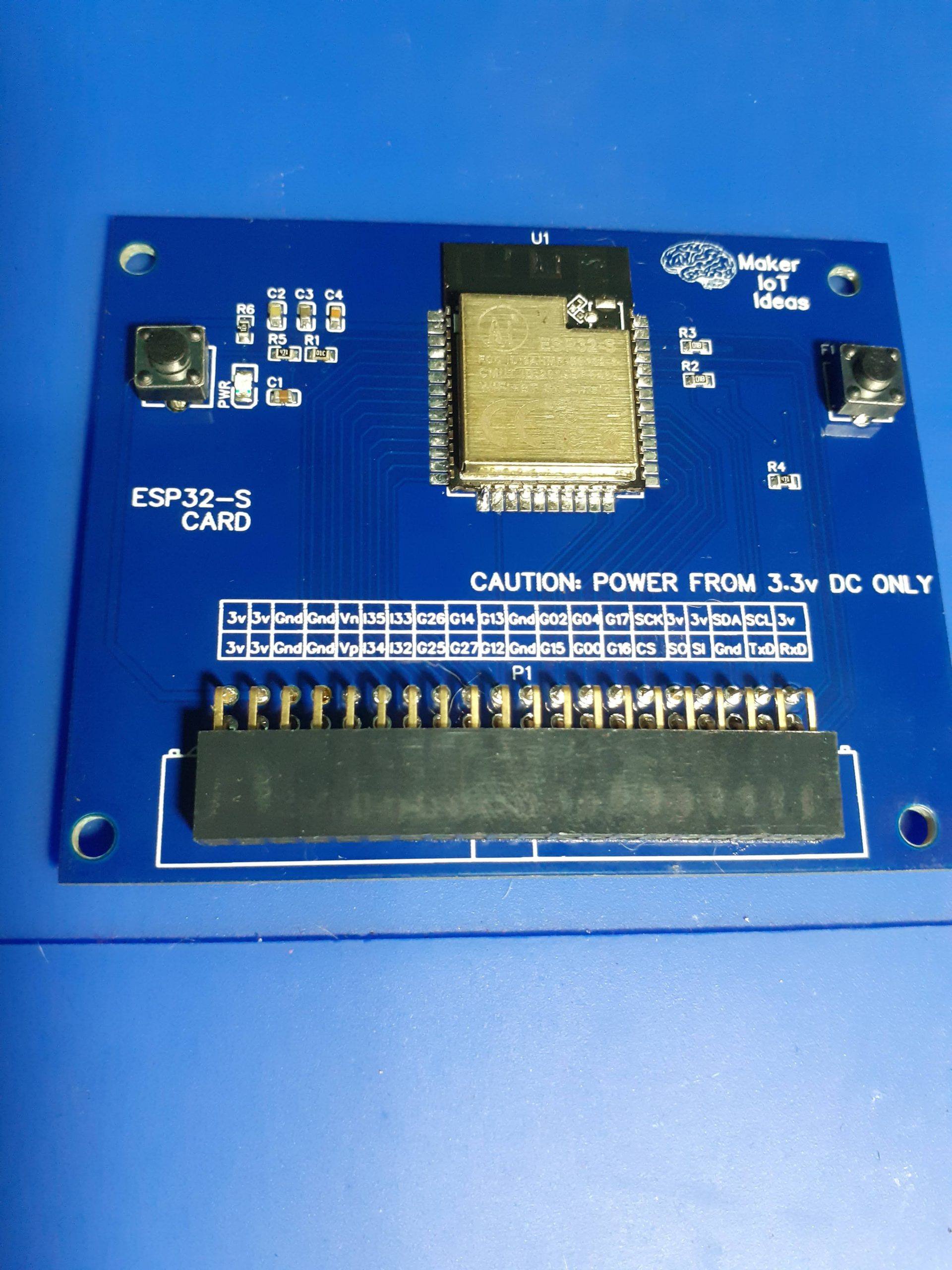
The Assembly
To make things easier for them, I had previously selected all components, and together with a label and component designators, placed each component into a separate anti-static plastic bag. This achieved two things – it shielded the students from having to handle reels of components, potentially resulting in a lot of wastage, and it make it almost impossible to place a wrong component in a wrong place, as each of the bags were clearly marked with the specific component designator of the component it contained.
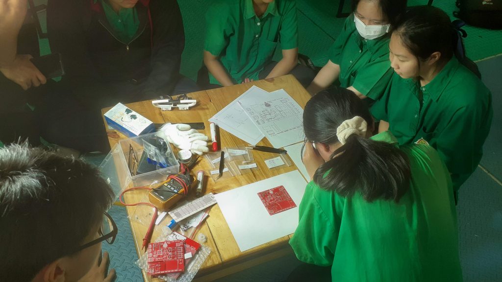
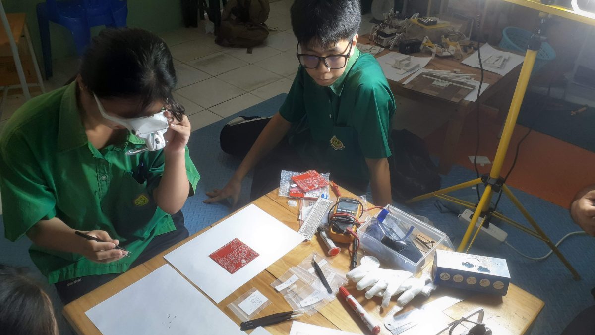
Their feelings of “dismay” were quickly replaced with wonder as I used a stencil to apply solder paste to the PCB. There were also confusing present, as they could not understand how the “sticky” solder would melt and keep the component in place. They were also quite worried about placing the components onto the PCB – that was until they saw that there was a selection of fine tweezers set out to use for exactly this purpose…
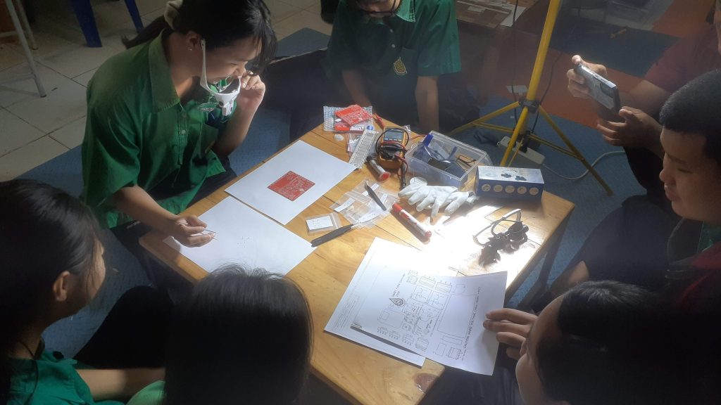
They now became very excited and took turns to each place a few components onto the PCB. I took special care to keep the diodes, optic isolators and microcontroller well away from them, at least until I explained that these components were polarised, or had to be placed in a specific orientation onto the board.
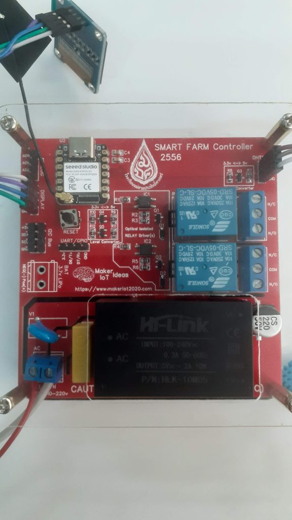
After a bit of struggling with the diodes, as well as the microcontroller, all the SMD components were eventually correctly placed onto the PCB. I now took over and used a hotplate to reflow the PCB.
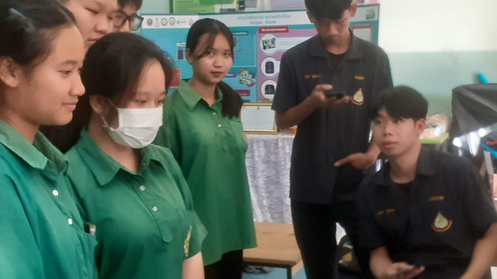
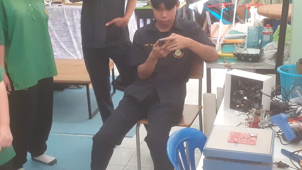
This process completely amazed them, or at least, most of them, as some took this opportunity to continue with the ever present interaction of students and mobile phones that are so common in SE Asia 🙂
The PCB was now reflowed, and after a short break to let things cool down, we continued with the soldering and assembly of the through-hole components.
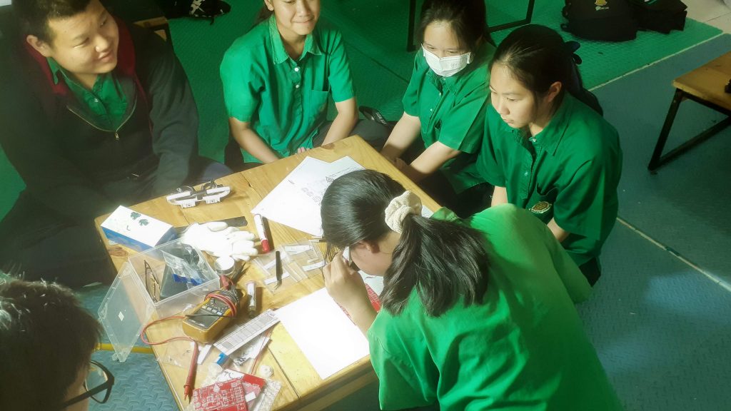
The proceedings would not be complete without a group photo of the students and the PCB that they assembled.
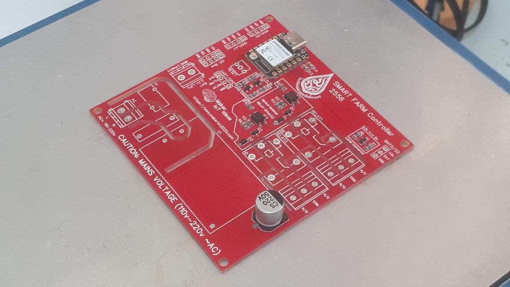
Conclusion of part 2
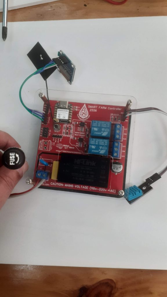
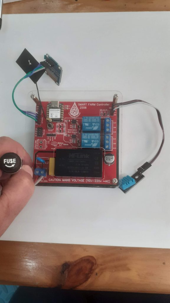
With the PCB now assembled, I used my desktop CNC machine to cut acrylic plastic to form a protective shell. The PCB will soon be installed at the remote site shown in part 1, and while it will be inside a IP65 electrical enclosure, I still felt the need for a little bit of added protection.
The firmware development is complete, and we are currently busy bringing the students up to date with the exact operation thereof. Our goal is that they would at least try to create their own version of the firmware for use in the electronics lab, as well as a comparison between my version of the firmware and theirs.
From the smiles on their faces during the entire process, it was quite obvious that they really enjoyed this project.