I2C between Maker Nano and Kid-Bright32 (Esp32)

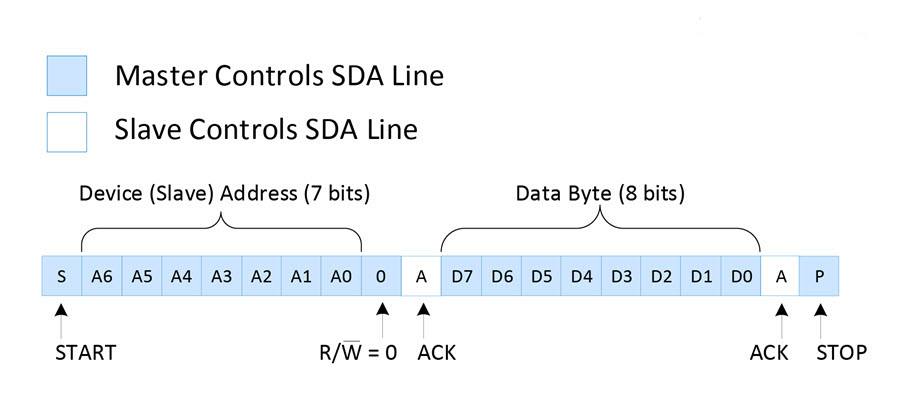
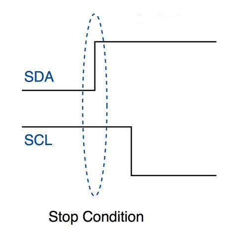
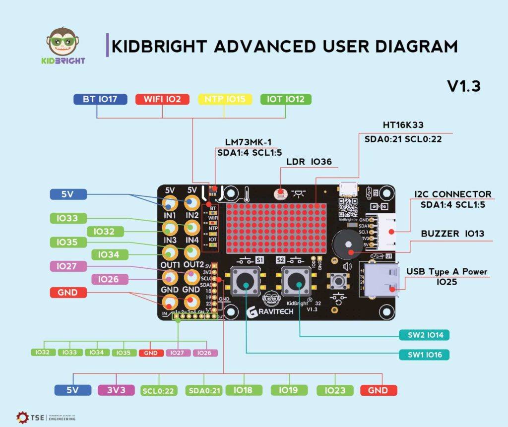
In our last post, we started looking at the workings of the I2C protocol. In case you missed that, you can read about that here. Today, I will continue with I2C by showing you how to implement the protocol between an Maker Nano (a Arduino Nano Clone) and Kid-Bright32 (a ESP32 based development and Education device).

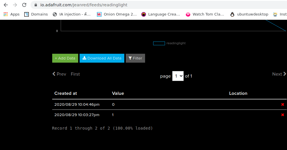
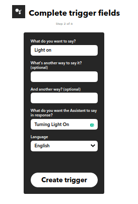
This project will eventually be turned into an IoT device, with Google Assistant voice control. The Kid-Bright have very limited IO pins, and the Maker Nano has no Network Connectivity unless we use an Ethernet Shield. Enough of that for now, let us start with today’s tutorial, we will get back to this project later…

The Code for the Master

/* I2C Master Code - Kid Bright 32 v 1.3
   Can be adapted to Arduino or NodeMCU or STM32
   As it uses no special libraries, only the standard Wire.h
   that is already included with the Arduino IDE
*/

#include <Wire.h>

#define button1 16 // Button 1
#define button2 14 // Button 2
#define led_blue 17 // Led 1
#define led_red 2 // Led 2
#define led_yellow 15 // Led 3


void setup() {
  Wire.begin(); // Start I2C, join bus as a Master
  pinMode(button1,INPUT_PULLUP); // Set as input
  pinMode(button2,INPUT_PULLUP); 
  pinMode(led_blue,OUTPUT); // Set as output
  pinMode(led_red,OUTPUT);
  pinMode(led_yellow,OUTPUT);
  digitalWrite(led_blue,HIGH); // LED is Active Low
  digitalWrite(led_red,HIGH); // LED is Active Low
  digitalWrite(led_yellow,HIGH); // LED is Active Low
  Serial.begin(115200); // Start Serial for debugging
}

byte Data = 0; // Variable for sending data to the slave
int SlaveData = 0; // Variable for receiving data from the slave

void loop() {
  Wire.beginTransmission(4); // Send data to Slave at address #4
  Wire.write(Data); // Transmit one byte ( 8 bits)
  Wire.endTransmission(); // End Transmission
  Wire.requestFrom(4,1); // Request one (1) byte of data from the      //slave at address$
  while (Wire.available()) { // If data received
    SlaveData = Wire.read(); // Save it into a variable
  }

// We will implement a simple latch in software, where a single 
// button latches or releases a bit with every press and release.  
// This code should ideally include debouncing as well. It was left
// out for clarity.

  if (digitalRead(button1) == LOW) { // If button 1 pressed
    if (bitRead(Data,0) == HIGH) { // test if bit 0 in variable is set
      bitClear(Data,0); // clear it if it is set
    } else {
      bitSet(Data,0) == HIGH; // set bit to high
    }
  } 
// Do the same for the second button

  if (digitalRead(button2) == LOW) {
    if (bitRead(Data,1) == HIGH) {
      bitClear(Data,1);
    } else {
      bitSet(Data,1) == HIGH;
    }
  } 
 
// We will test for a set bit in the transmitted byte, and invert it, 
// as the LED's are active LOW

  digitalWrite(led_blue,!bitRead(Data,0)); // Toggle Led 1
  digitalWrite(led_red,!bitRead(Data,1)); // Toggle Led 2

// Same with the data received from the slave

  digitalWrite(led_yellow,!bitRead(SlaveData,0)); // Toggle Led 3
  
// Print Debug info on serial port
  
  Serial.print("Send to Slave 0xb");
  Serial.println(Data,BIN);
  Serial.print("Received from Slave 0xb");
  Serial.println(SlaveData,BIN);
  
 // Small delay, should change to millis in production code

  delay(200);
       
}
The Master Device. Connections are +5v (red) SCL (brown) SDA (orange) Ground (blue)

Code for the Slave

/*
     I2C Slave
     Arduino Nano or Compatible, can be used with ESP32 or STM32
     as well as no special libraries used, only standard Wire.h
*/

#include <Wire.h>

#define button 2 // A user button
#define led1 3 // Led 1
#define led2 4 // Led 2

byte Data = 0; // Variable for sending data to the Master

void setup() 
{
  pinMode(button,INPUT_PULLUP); // Set as Input
  pinMode(led1,OUTPUT);
  pinMode(led2,OUTPUT);
  digitalWrite(led1,LOW); // Led is Active High, so switch it off
  digitalWrite(led2,LOW);
  Wire.begin(4); // Join I2C Bus as device #4
  Wire.onReceive(receiveEvent); // Register receive Event
  Wire.onRequest(requestEvent); // Register request event
  Serial.begin(115200); // start serial debugging
  
}

void loop() {
// implement a software bit latch, on bit 0 of the Data variable
// the latch is toggled by pressing and releasing the button
// should ideally be debounced as well

 if (digitalRead(button) == LOW) {
  if (bitRead(Data,0) == HIGH) {
    bitClear(Data,0);
  } else {
    bitSet(Data,0) == HIGH;
  }
 }
 delay(200); // small delay
}

// This event will be triggered when the master requests data

void requestEvent() 
{
  Wire.write(Data); // Send data to the master
  Serial.print("Sending to Master 0xb");
  Serial.println(Data,BIN);
}
// This event gets triggered when the master sends data

void receiveEvent(int Quantity)
{
  int x = Wire.read(); // read the data ( one byte in this case)
  digitalWrite(led1,bitRead(x,0)); // Toggle LED 1 on Bit 0 state
  digitalWrite(led2,bitRead(x,1)); // Toggle LED 2 on Bit 1 state
  Serial.print("Received from Master 0xb"); // Debugginh
  Serial.println(x,BIN);

}
Maker Nano on an IO Shield, Connections are +5v (red) SCL (brown) SDA (orange) Ground (blue)

How does this work.

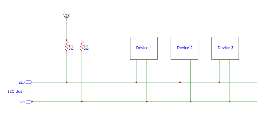
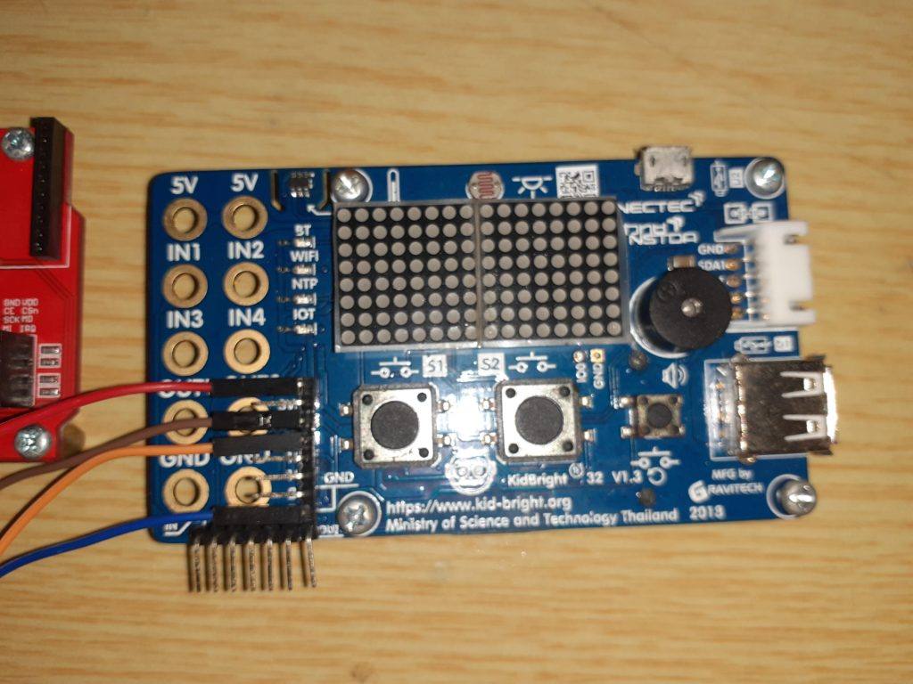
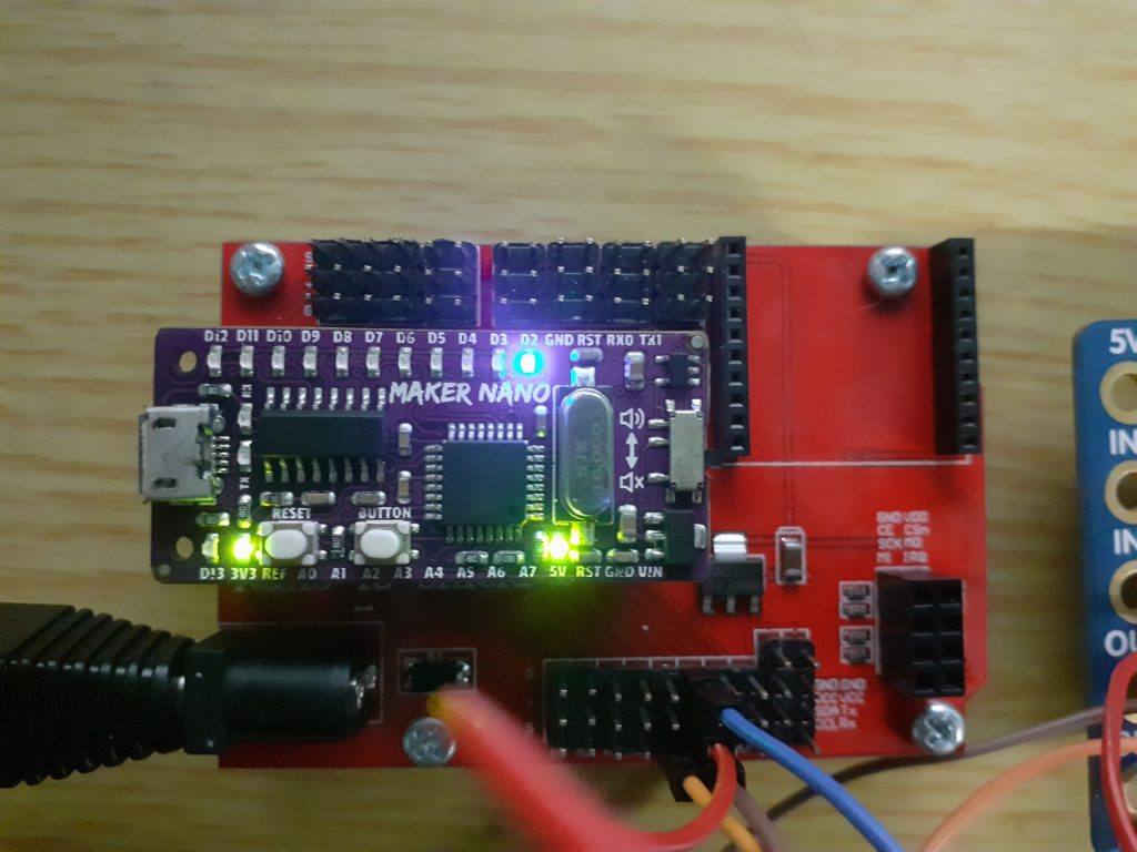
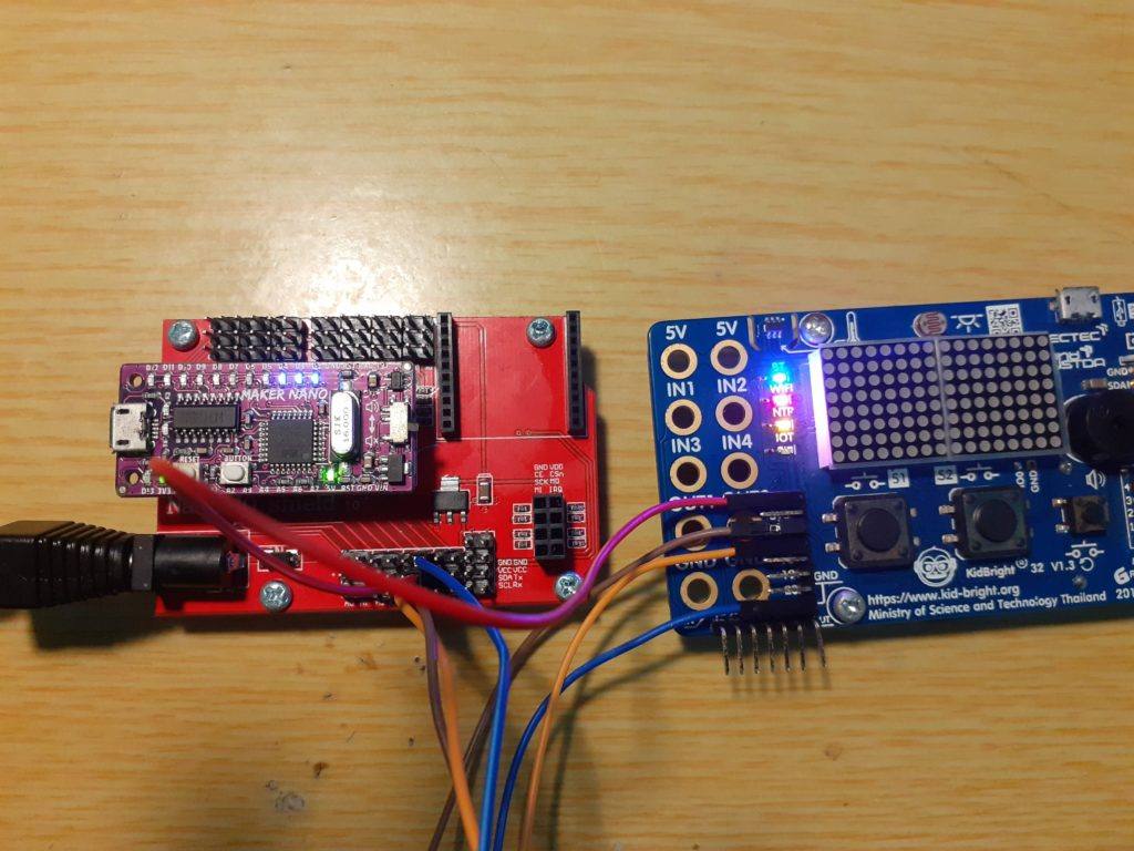
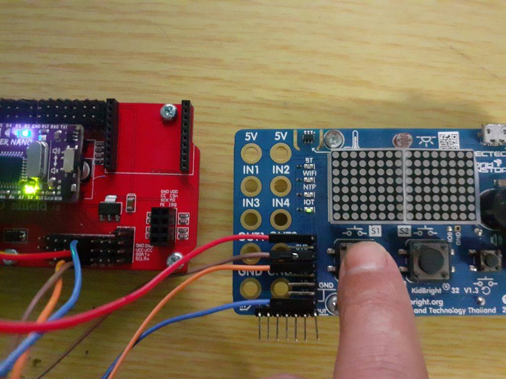
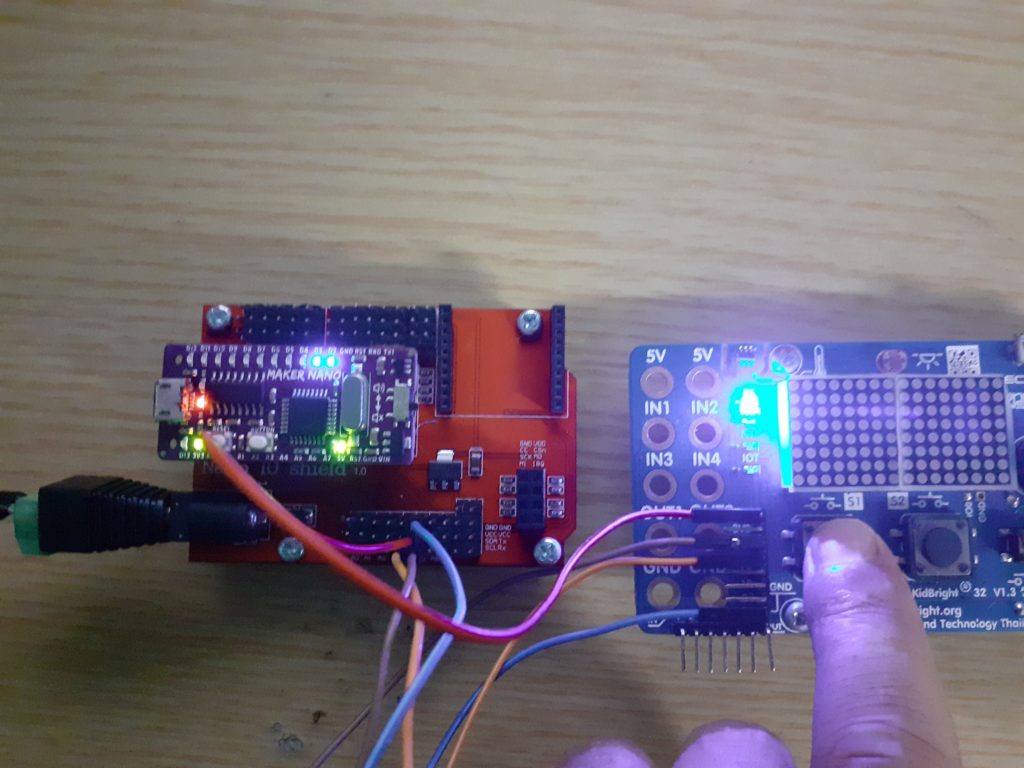
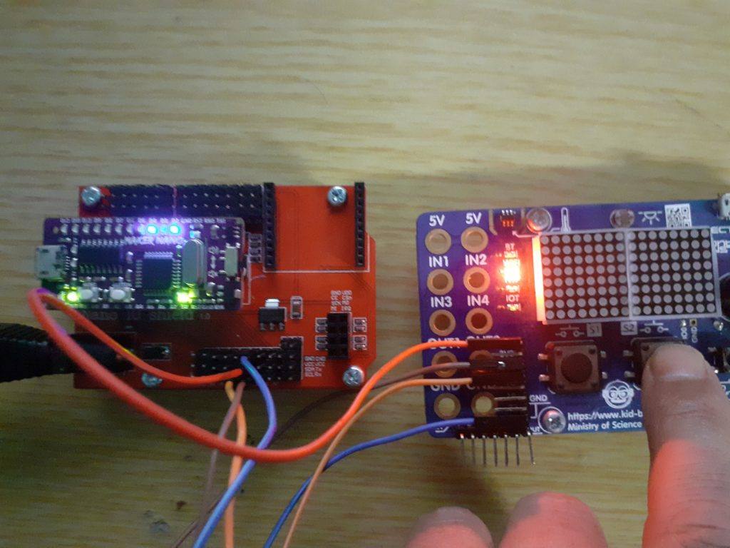
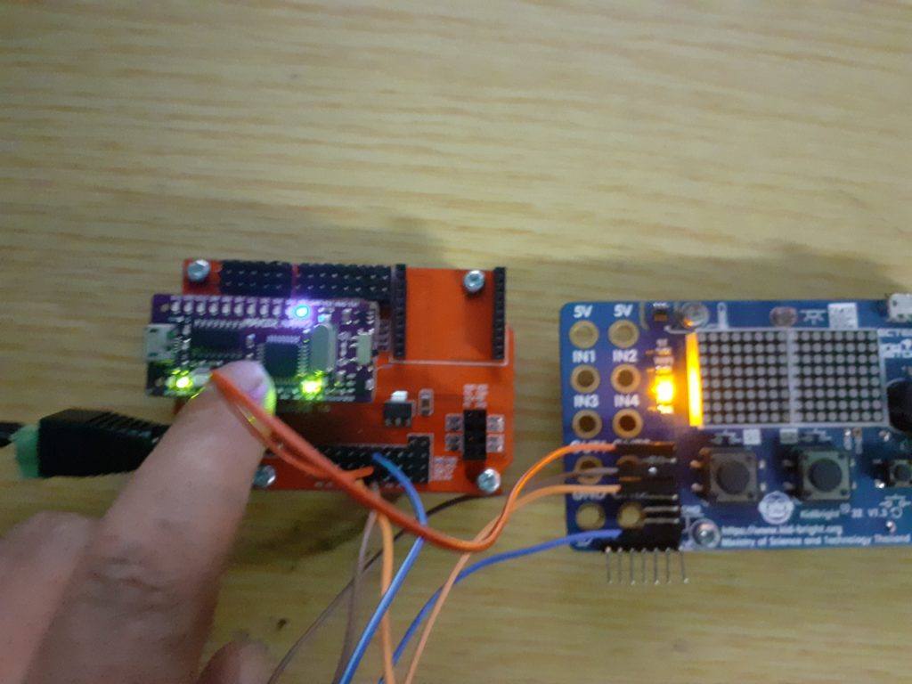
After uploading the code to the two boards, and connecting the boards to the I2C bus, we may power everything up. Please note that the boards MUST have a common ground. I have also powered both from the same supply. also make sure the SDA goes to SDA, and SCL to SCL… On a short distance like this, pull-up resistors are not required ( your milage may vary )

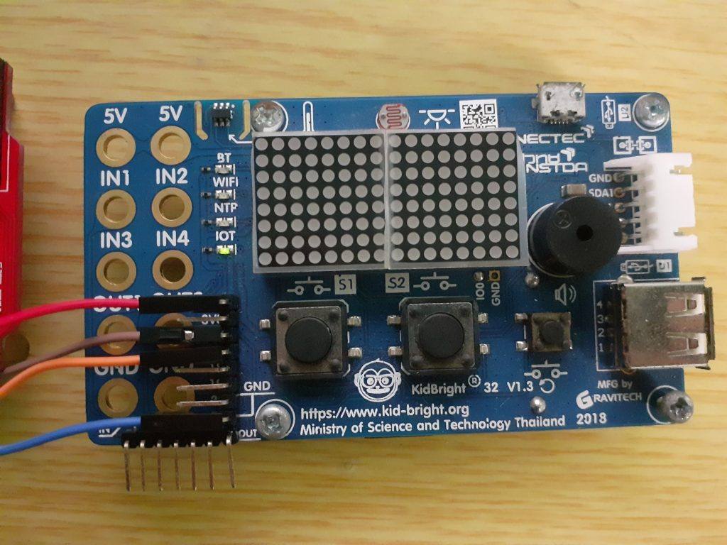
When we first power it up, is will seem as if nothing happened, but if you press and release one of the switches, the LED’s will light up, and stay lit until you press the switch again.

What next ?

In further parts of this, we will expand on this device, turning it into an IoT device, by combining many different skills that I have presented in previous tutorials.

What exactly is I2C?

In this post, I will tell you all the basics of the I2C protocol. What it is, where it comes from and also how it is configured and setup. We will also look at how data is transferred and received

Table of contents
1. Introduction
2. The Features of I2C
3. The Hardware
3.1 The physical I2C Bus
3.2 The Master and Slave devices on the bus
4. The data transfer protocol
4.1 The Start Condition
4.2 The Address Block
4.3 The Read/Write Bit
4.4 The ACK/NACK Bit
4.5 The Data Block
4.6 The Stop Condition
5. How does I2C work in practice
5.1 Sending data to a Slave Device
5.2 Reading data from a Slave Device
5.3 The Clock stretching concept

Introduction

I2C communication is the short form name for inter-integrated circuit protocol. It is a communication protocol developed by Philips Semiconductors for the transfer of data between a central processor and multiple integrated circuits on the same circuit board by using just two common wires.

Due to its simplicity, it is widely adopted for communication between microcontrollers and sensor arrays, displays, IoT devices, EEPROMs etc.

This is a synchronous serial communication protocol. It means that data bits are transferred one by one at regular intervals of time set by a reference clock line.

The Features of I2C

The I2C protocol has the following important features

  • Only two common bus lines (wires) are required to control any device/IC on the I2C network.
  • There is no need for a prior agreement on data transfer rate like in UART communications. The data transfer speed can thus be adjusted whenever it is required.
  • It has a simple mechanism for validating the transferred data.
  • It uses a 7-bit addressing system to target a specific device/IC on the I2C bus.
  • I2C networks are extremely easy to scale. New devices can simply be connected to the two common I2C bus lines.

The Hardware

The physical I2C Bus

The I2C Bus (Interface wires) consists of just two wires and are named Serial Clock Line (SCL) and Serial Data Line (SDA). The data to be transferred is sent through the SDA wire and is synchronized with the clock signal from SCL. All the devices/ICs on the I2C network are connected to the same SCL and SDA lines as shown in the image below:

The physical I2C Bus. All devices are connected to the same 2 wired on the bus, namely SDA and SCL

Both the I2C bus lines (SDA, SCL) are operated as in open-drain driver mode. It means that any device/IC on the I2C network can drive(pull) SDA and SCL low, but they cannot drive them high. So, a pull-up resistor is used on each bus line, to keep them high (at positive voltage) by default.

This is to prevent the bus from shorting, which might happen when one device tries to pull the line high and some other device tries to pull the line low.

The Master and Slave Devices on the I2C Bus

The devices connected to the I2C bus are categorized as either masters or slaves. At any instant of time, only a single master stays active on the I2C bus. It controls the SCL clock line and decides what operation is to be done on the SDA data line.

All the devices that respond to instructions from this master device are slaves. For differentiating between multiple slave devices connected to the same I2C bus, each slave device is physically assigned a permanent 7-bit address.

When a master device wants to transfer data to or from a slave device, it specifies this particular slave device address on the SDA line and then proceeds with the transfer. So effectively communication takes place between the master device and a particular slave device.

All the other slave devices don’t respond unless their address is specified by the master device on the SDA line.

The Master and Slave Devices on the I2C Bus. Note that each Slave device has it’s own address.

The Data Transfer Protocol

The protocol (set of rules) that is followed by the master device and slave devices for the transfer of data between them works as follows:

Data is transferred between the master device and slave devices through the SDA data line, via patterned sequences of 0’s and 1’s (bits). Each sequence of 0’s and 1’s is called a transaction and each data transaction is structured as in the image below:

The structure of an I2C Data transaction

The Start Condition

Whenever a master device/IC decides to start a transaction, it switches the SDA line from a high level to a low level before the SCL line switches from high to low.

Once a start condition is sent by the master device, all the slave devices get active even if they were in sleep mode, and wait for the address bits to see which device should respond.

The I2C Start Condition. Note that SDA Switches LOW before SCL. All slave devices on the bus will now listen for an address bit to decide which device should respond.

The Address Block

The Address block is comprised of 7 bits and are filled with the address of slave device (in binary) to/from which the master device needs to send/receive data. All the slave devices on the I2C bus will compare these address bits with their own address.

The Read/Write Bit

This bit specifies the direction that the data must be transferred in. If the master device/IC needs to send data to a slave device, this bit is set to ‘0’. If the master device/IC needs to receive data from the slave device, it is set to ‘1’.

The ACK/NACK Bit

This is the Acknowledged/Not-Acknowledged bit. If the physical address of any slave device is the same as the address that was broadcasted by the master device, that slave device will set the value of this bit to ‘0’ . If there are no slave device(s) with the broadcasted address, this bit will remain at logic ‘1’ (default). This will tell the master that the data/command has been received and/or acknowledged by a slave device.

The Data Block

The data block is comprised of 8 bits and they are set by the transmitter,wheather this be the master or the slave, depending on wheather a read or a write operation was requested, with the data bits that needs to transfered to the receiver. This block is followed by an ACK/NACK bit that is set to ‘0’ by the receiver if it successfully receives data. Otherwise it stays at logic ‘1’.

This combination of data blocks followed by an ACK/NACK bit is repeated until all the data is completely transferred.

The Stop Condition

After all the required data blocks are transferred through the SDA line, the master device switches the SDA line from low to high before the SCL line switches back from high to low.

The I2C Stop condition. This signals the end of a transaction. Note SDA returns to High BEFORE the SCL line is pulled High.

How does I2C work in practice

When an I2C transaction is initiated by a master device either to send or receive data to/from a slave device, all of the processes mentioned above will happen at least one.
Let us look at a typical scenario for each of the different type of scenarios.

Sending Data to a Slave Device

The following sequence of operations will take place when a master device tries to send data to a particular slave device through I2C bus:

  • The master device sends a start condition
  • The master device sends the 7 address bits which correspond to the slave device to be targeted
  • The master device sets the Read/Write bit to ‘0’, which signifies a write
  • Now two scenarios are possible:
    • If no slave device matches with the address sent by the master device, the next ACK/NACK bit stays at ‘1’ (default). This signals the master device that the slave device identification is unsuccessful. The master clock will end the current transaction by sending a Stop condition or a new Start condition
    • If a slave device exists with the same address as the one specified by the master device, the slave device sets the ACK/NACK bit to ‘0’, which signals the master device that a slave device is successfully targeted
  • If a slave device is successfully targeted, the master device now sends 8 bits of data which is only considered and received by the targeted slave device. This data means nothing to the remaining slave devices
  • If the data is successfully received by the slave device, it sets the ACK/NACK bit to ‘0’, which signals the master device to continue
  • The previous two steps are repeated until all the data is transferred
  • After all the data is sent to the slave device, the master device sends the Stop condition which signals all the slave devices that the current transaction has ended

The image below represents the transaction with the data bits sent on the SDA line and the device that controls each of them:

I2C Master sending data to a slave device

Reading Data from a Slave Device

The sequence of operations remain the same as in previous scenario except for the following:

  • The master device sets the Read/Write bit to ‘1’ instead of ‘0’ which signals the targeted slave device that the master device is expecting data from it
  • The 8 bits corresponding to the data block are sent by the slave device and the ACK/NACK bit is set by the master device
  • Once the required data is received by the master device, it sends a NACK bit. Then the slave device stops sending data and releases the SDA line

If the master device to read data from specific internal location of a slave device, it first sends the location data to the slave device using the steps in previous scenario. It then starts the process of reading data with a repeated start condition.

The below figure represents the overall data bits sent on the SDA line and the device that controls each of them:

Reading data from a Slave device on the I2C bus

The Clock Stretching concept

Let say the master device started a transaction and sent address bits of a particular slave device followed by a Read bit of ‘1’. The specific slave device needs to send an ACK bit, immediately followed by data.

But if the slave device needs some time to fetch and send data to master device, during this gap, the master device will think that the slave device is sending some data.

To prevent this, the slave device holds the SCL clock line low until it is ready to transfer data bits. By doing this, the slave device signals the master device to wait for data bits until the clock line is released

Conclusion

This concludes this tutorial. In a future post, I will show you how to use I2C to transfer data between two micro-controllers.


ESP32 (Kid Bright v 1.3) Voice-Activated IoT Relay Control using IFTTT and Adafruit IO

Today I will show you how to do a very quick IoT relay controller using IFTTT and Adafruit IO. I will be using the Kid Bright v 1.3 Development board, from Gravitec in Thailand. These boards sell for about $USD 25 to 35 each, quite expensive as far as I am concerned, for the amount of functionality that you get.

I will also post a link to the Video Tutorial at the bottom of this tutorial.

Kid Bright v 1,3 Development Board, Advanced user Diagram
Kid Bright 32 Schematic

You can find out more about this board on the Kid Bright Website. Please note that you will need Google Translate, as the site is in the Thai Language.

We will use IFTTT to connect Google Assistant to Adafruit IO in order to control our IoT Relay controller with voice commands.

Let us start our project.

Start the Arduino IDE, and make sure that you have enabled support for NodeMCU or other ESP32 based processors.
You also need to load the libraries for Adafruit IO.

After you have done that, open the “adafruitio_07_digital_out” sketch from the Examples folder for Adafruit IO. We will modify this example to suit our needs, as well as save some time on coding.

Change the Example to the following:
Remember to change the pins to reflect your particular setup.

include “config.h”

define LED_PIN 17
define Relay 27

// set up the ‘readinglight’ feed
AdafruitIO_Feed *readinglight = io.feed(“readinglight”);

void setup() {

pinMode(LED_PIN, OUTPUT);
pinMode(Relay, OUTPUT);

// start the serial connection
Serial.begin(115200);

// wait for serial monitor to open
while(! Serial);

// connect to io.adafruit.com
Serial.print(“Connecting to Adafruit IO”);
io.connect();

// set up a message handler for the ‘readinglight’ feed.
// the handleMessage function (defined below)
// will be called whenever a message is
// received from adafruit io.
readinglight->onMessage(handleMessage); // Handler for our FEED

// wait for a connection
while(io.status() < AIO_CONNECTED) {
Serial.print(“.”);
delay(500);
}

// we are connected
Serial.println();
Serial.println(io.statusText());
readinglight->get();

}

void loop() {

// io.run(); is required for all sketches.
// it should always be present at the top of your loop
// function. it keeps the client connected to
// io.adafruit.com, and processes any incoming data.
io.run();

}

// this function is called whenever an ‘readinglight’ feed message
// is received from Adafruit IO. it was attached to
// the ‘digital’ feed in the setup() function above.
void handleMessage(AdafruitIO_Data *data) {

Serial.print(“received <- “);

if(data->toPinLevel() == HIGH)
Serial.println(“HIGH”);
else
Serial.println(“LOW”);

digitalWrite(LED_PIN, !data->toPinLevel()); // We inverse the logic on the LED, we want it on //when the relay is on, and off when the relay is off
digitalWrite(Relay, data->toPinLevel()); // My Relay Module is Active LOW, so this is correct.
//reverse the logic if your module is Active High
}

Another very important step is that you need to set your Adafruit IO IO-Key in the config.h file. Your Wifi SSID and Password also needs to be supplied here, to enable your ESP32 based processor to connect to Adafruit through your WiFi connection.

Config.h

/ Adafruit IO Config */
define IO_USERNAME “your AdafruitIO username”
define IO_KEY “your AdafruitIO IO Key”
define WIFI_SSID “your wifi ssid”
define WIFI_PASS “your wifi password”

Leave everything else as is in the config.h file

Now login to Adafruit IO, or create a new account if you have not done so already.
Create a new feed, in my case called readinglight, under your feeds.

Click on the Adafruit IO Key button ( top right corner ) and copy your IO Key and Username into the config.h file in the Arduino IDE. Don’t upload your code yet.

Now go to IFTTT, and login or create a new account if you don’t have one already.
After you have logged in, in a new window, go to https://www.ifttt.com/adafruit

Make sure to connect Adafruit and IFTTT, and allow IFTTT to send messages to Adafruit IO.

Then, follow the pictures, and create your first applet.

Select “Say a Simple phrase”
Configure it with what you want to say to activate the relay, Then Click “Create Trigger”
Click on :Adafruit”
Click Send Data to Adafruit IO
Select you feed from the drop-down box. IMPORTANT, USE A 1 to switch something ON, or a 0 to switch it OFF. HIGH AND LOW, or ON and OFF DOES NOT WORK ! Then Click on Create Action
Review your applet, Switch OFF notifications, and Click on Finish.

Now create another Applet, Doing exactly the same, but change your wording to “Light OFF” and the Adafruit IO Data to 0. This applet will be used to switch off the Relay.

Go back to the Feed window in Adafruit IO, and then test Google Assistant by saying your command, like “Hey Google, Light On” and “Hey Google, Light Off”

You should see data arriving in your feed window after each command. A 1 for On and a 0 for Off.

Now go back to your Arduino IDE, Open the Serial Monitor, and Compile and Upload your Code. Test it again, but now you should see data arriving in the Serial Monitor as well.

If all of this is working, You can connect your Relay to the board, and test it again.
When you are happy that all is working as it should, Connect a load to the relay, and enjoy your new Voice-Activated IoT Relay Controller.

It is also easy to add another feed to the existing code. Ask me how if you don’t understand, but it should be quite easy to figure out from the code as well 🙂

https://youtu.be/Q-uwU55VAF4
Voice Controlled IoT Relay controller using Google Assistant, IFTTT and Adafruit IO

Extending Arduino/Esp32/STM32 GPIO Pins – PART 2

In the first part of this series, I showed you how to extend the available output pins on your microprocessor by using a SIPO (Serial In, Parallel Out) Shift Register. These work great to extend your outputs, but they do tend to involve a bit of extra work and organisation in your code. They are also a bit slower than the normal GPIO pins, because data has to be serially shifted into them, and then latched out onto the parallel port.

I have also mentioned that there are I2C devices available that can make this much easier… In today’s article, I will show you how to use one of these I2C devices, the PCF8574.

These little modules have some quite impressive features, for one, allowing you to cascade up to 8 of them together, giving you a quite impressive 64 GPIO ports ! I am also happy to tell you, that if you can find the PCF8574A variant, as well, you can increase the total amount of ports to 128! ( If you chain 8x PCF8574 as well as 8x PCF8574A together) This is possible because the I2C addresses of the two series of chips are different. Thus allowing us to add a total of 16 of them to the I2C bus.

It must however be said that you should calculate your bus resistance very carefully if you plan on doing that. For most of us, I do not believe we will need that much GPIO on a single microprocessor!

Enough introduction, let us start by looking closely at the chip, as well as the modules that you can purchase for around 1 USD each…

A word of caution, there is also another version of these available, which is specifically designed to be used with LCD screens. You should thus be careful when you buy a premade module, that you choose the io-extender version, and not the LCD controller version.

PCF8574 I2C IO Extender module – Front View
PCF8574 I2C IO Extender – Back View

As we can see, the GPIO ports are clearly labeled, from P0 to P7, with the INT (Interrupt Pin) on the very right.

As I have said before, you can cascade up to 8 of these onto the I2C bus. This is done by setting the I2C address of the module. This is done by setting the jumpers as seen in the picture below.

Address Jumpers on the PCF8574 I2C IO Extender Module

The Address can be set by using the following table to lookup the address and set the jumpers accordingly.

A2A1A0I2C Device Address
0000x20
0010x21
0100x22
0110x23
1000x24
1010x25
1100x26
1110x27
Available I2C Addresses for PCF8574 selected by setting the jumpers

Connecting the device is very easy. You only have to supply 5v and Ground, as well as connect it to the SCL and SDA Pins on your microprocessor. For Arduino Uno / Nano that is A4 (SDA) and A5 (SCL)

As far as the coding is concerned, you have two options. You can either use the built-in Wire library, or you can download a special library. Both works equally well, but I do believe that the built-in Wire library might be a little bit faster.

Another point to make is that there are a lot of “fake” modules on the market these days. These modules work, but some of them have extremely weak current sourcing abilities. ( I recently bought a pair online, and they are unable to properly light an LED even without a current limiting resistor. I fixed that issue by driving the LED through a small BJT transistor, like the 2n2222a.

You should also take note that the ports will start up in a weak HIGH state when the module is powered up. This should be taken into consideration when designing your circuit to drive external devices through the outputs. In other words, you should take precautions to prevent the devices from switching on before the microprocessor takes control of the module.

Let us start to look at the coding that you will need to do to use this device.
I will start with the built-in wire Library that is included with the Arduino IDE.

#include <Wire.h> // Wire.h provide access to I2C functions

void setup()
{
Wire.begin(); // Start I2C
}

void loop()
{

Wire.beginTransmission(0x20); // Our device is on Address 0x20
Wire.write(0x0F); // This is equal to 0b00001111, meaning it will switch ports P0 to P3 High
Wire.endTransmission();
delay(1000);
Wire.beginTransmission(0x20);
Wire.write(0xF0); // This is equal to 0b11110000, meaning it will switch ports P4 to P7 High
Wire.endTransmission();
delay(1000);
}

The code above will alternate between switching 4 ports high and low every one second.
You can observe this by connecting 8 LEDs through 330ohm resistors to ports P0 through P7


Reading the status of a port (meaning that you configured it as an input) can be done using the following code

#include<Wire.h>

void setup()
{
  Serial.begin(9600);
  Wire.begin();
  Wire.beginTransmission(0x20);
  Wire.write(0x00);  //LED1 is OFF
  Wire.endTransmission();
}

void loop()
{
  Wire.requestFrom(0x20, 4); // Read the state of P4
  byte x = Wire.read();
  if (bitRead(x, 4) == LOW)
  {
    Wire.beginTransmission(0x20);
    Wire.write(0x01);  //LED1 is ON
    Wire.endTransmission();
  }
  else
  {
    Wire.beginTransmission(0x20);
    Wire.write(0x00);  //LED1 is OFF
    Wire.endTransmission();
  }
  delay(1000);
}

This code assumes that you have connected a LED throught a resistor to P0, and that you have connected a pullup resistor of 10k to P4, with a pushbutton to GROUND.

The LED should switch on when you press the switch, and go off again once you release it.

If you want to use the special library, you can download it below:

Install this into your Arduino Libraries, and use the following code:

include “Arduino.h”

include “PCF8574.h

// Set i2c address
PCF8574 pcf8574(0x20);

void setup()
{
Serial.begin(115200);

// Set pinMode to OUTPUT

pcf8574.pinMode(P0, OUTPUT);

pcf8574.begin();

}

void loop()
{
pcf8574.digitalWrite(P0, HIGH);
delay(1000);
pcf8574.digitalWrite(P0, LOW);
delay(1000);
}

Reading the status of an Input can be done like this:

include “Arduino.h”

include “PCF8574.h”

// Set i2c address
PCF8574 pcf8574(0x20);

void setup()
{
Serial.begin(115200);

pcf8574.pinMode(P0, OUTPUT);
pcf8574.pinMode(P1, INPUT);
pcf8574.begin();

}

void loop()
{
uint8_t val = pcf8574.digitalRead(P1);
if (val==HIGH) Serial.println(“KEY PRESSED”);
delay(50);

}

There are also excellent examples included with the library. These include using the interrupt pin.

I hope that this will be useful to somebody.

Extending the Inputs and Outputs of your Arduino/ESP32/STM32

There will come a time that you will run out of available input or output pins on your Arduino/ESP32 or STM32 device. Today, I will show you one way to work around this problem and how to add additional input and/or outputs to your device.

There are many ways to do this, the easiest of them being adding some sort of i2c
chip (the Waveshare PCF8574 IO Expansion Board is a good example).

This particular device can be cascaded to provide up to 64 IO ports on the i2c bus.

At Maker and IoT Ideas, we would however like to show you electronics that you can build yourself, or stuff that have not already been made up into some kind of commercial project.

So, keeping this DIY attitude going, I will teach you how to use a shift register today.

Before we do that, we have to look at what a shift register is, and how they work…

A shift register, at its basic level, is actually just a series of D Type Flip-Flops.

D Type Flip Flop

These flip flops are connected together to give this

Parallel in, Serial out Shift Register

There are three basic types of Shift Register
– Serial In, Serial Out (SISO)
– Serial In, Parallel Out (SIPO) and
– Parallel In, Serial Out (PISO)

We can see that they these type of shift registers are mainly used to convert between an serial and parallel data interface.

Serial In, Serial Out ( SISO)

This is the easiest configuration for a shift register. It is basically just a row of flip flops, with the output of the first, connected to the input of the next… and so on. This type of shift register is mainly used to introduce a delay into the data stream. This means that for a 8 bit SISO Shift register, the first data will only appear at the output after 8 clock cycles !

Serial In, Parallel Out (SIPO)

This kind of Shift Register has the same configuration as the SISO type, but it differs in that there is output after every flip-flop. That makes this type of shift register a good choice to use to extend the outputs on a microcontroller like Arduino or ESP32. The downside of using a shift register as a parallel output device is that the outputs will be slightly slower than if you used the native outputs on the microcontroller.

Parallel In, Serial Out (PISO)

A Parallel In, Serial out shift register can be used to read inputs from buttons or other digital devices. These inputs are then serially shifted into a serial pin on the microcontroller to be processed. It is also slightly slower than if you used the native inputs on the microcontroller.

Universal Shift register

You are also able to use a universal shift register. These chips can be used as both inputs and outputs. They are however only available in a 4 bit configuration.

The Chips (IC’s)

TYPELOGICCHIP NUMBERBITS
SISO / SIPOTTL74HC5958 bit
SIPOTTL74LS1648 bit
PISOTTL74HC1668 bit
UNIVERSALTTL74LS1944 bit
UNIVERSALTTL74LS1954 bit
UNIVERSALCMOSCD40354 bit
Some common Shift Register Chips

Example using Arduino with 74HC595n SIPO Shift Register

We will look at an example to connect the 74HC5959N to Arduino to drive eight (8) LEDs.
This example can be adapted to drive other loads as well by using a small BJT transistor and current limiting resistor instead of the LED

74hc595n Pin NumberDescription and Connection
Q0…Q7 (15,1,2,3,4,5,6,7)Parallel outputs of the shift register to write up to 8 signals with only 3 pins on your Arduino or ESP32 microcontroller
GND (8)Connect to the ground on the microcontroller
VCC (16)Connect to 3.3V or 5V on the microcontroller
DS (14)Serial data input has to be connected to the microcontroller (in this example D4)
OE (13)Output enable input do we not need and connected to ground
STCP (Latch) (12)Storage register clock input has to be connected to the microcontroller (in this example D5)
SHCP (11)Shift register clock input has to be connected to the microcontroller (in this example D6)
MR (10)Master reset connected to VCC because is active with LOW and we do not want to reset the register
Q7S (9)Serial data output not needed and therefore not connected
Connections for 74HC595n to Arduino

The operation of the 74hc595n SIPO Shift Register can easily be explained in three steps:

  1. The latch (STCP pin) is pulled LOW because the data is only stored in the register on a LOW to HIGH transition of this pin.
  2. Data is shifted out to the register with the data pin (DS) and with a LOW to HIGH transition of the clock signal (SHCP).
  3. The latch (STCP pin) is pulled HIGH to save the data in the register.

Make the following connections to your Arduino and Breadboard ( we will use Arduino Nano today, but you can use the same pins and code for Arduino Uno )

Breadboard Layout for 74HC595 Shift Register as Output Extender with Arduino Nano
Schematic Diagram for using 74HC595 Shift Register as Output Extender with Arduino Nano

Double-check all your connections, and then you can start the coding. The code will be much easier than you may think, as there is already a builtin function in the Arduino C language that we will use to shift the data out to the register.

// Define the Control Pins for the register
int latch-Pin = 5;
int clock-Pin = 7;
int data-Pin = 6;

void setup()
{
pinMode(latch-Pin, OUTPUT);
pinMode(data-Pin, OUTPUT);
pinMode(clock-Pin, OUTPUT);

Serial.begin(9600);
}

void loop()
{
byte leds = 0;
updateShiftRegister();
delay(1000);
for (int i = 0; i < 8; i++)
{
bitSet(leds, i);
updateShiftRegister();
for (int i = 7; i >= 0; i–)
{
bool b = bitRead(leds, i);
Serial.print(b);
}
delay(1000);
Serial.println(” “);
}
}

void updateShiftRegister()
{
digitalWrite(latch-Pin, LOW);
shiftOut(data-Pin, clock-Pin, LSBFIRST, less);
digitalWrite(latch-Pin, HIGH);
}

In this example, we output a HIGH to each led in turn, shifting from 0 to 7.

I hope that this will make sense to everybody, and be useful.
Questions and comments are welcome. Next time, we will look as using a PISO Shift register to extend the inputs on you Arduino/ESP32/STM32

Thank you.

Using MQTT with IoT Devices – A Short Summary

You are excited, you have just finished your new IoT device, and have many excellent ideas on how you will use it remotely, on your smartphone, or even from your computer at the office. You now start thinking about how you will send and receive data to this new device of yours…

There are many ways that you can do this, but today, I would like to suggest a very easy and lightweight data transfer protocol. It is called MQTT. Some of you may already be using it, or you may at least have heard about it. Read on if you would like to know more about what it is, as well as how it works.

The History of MQTT

MQTT was designed by Andy Stanford-Clark (IBM) and Arlen Nipper (Cirrus Link, then Eurotech) in 1999. It was first used to monitor an oil pipeline running through the desert. The goal was to design and implement a protocol that is bandwidth-efficient, lightweight and uses very little battery power, because the devices were connected via satellite link which, at that time, was extremely expensive.

In 2013, IBM submitted the MQTT v3.1 protocol to the OASIS specification body with a charter that ensured that only minor changes to the specification could be accepted.MQTT-SN is a variation of the main protocol aimed at embedded devices on non-TCP/IP networks, such as Zigbee.

Historically, the “MQ” in “MQTT” came from the IBM MQ (then ‘MQSeries’) MQ product line. The protocol, however, provides publish-and-subscribe messaging (no queues, in spite of the name) and was specifically designed for resource-constrained devices and low bandwidth, high latency networks. This makes it an excellent candidate for data transmission on IoT and other low resource devices.

The Protocol Architecture (How does it work)

MQTT uses a client-server architecture, where the server is called the broker, and the client, called a client. The broker typically functions like a post office, in the sense that it doesn’t use the client’s address, but rather the subject of the topic that a client is subscribed to, to determine which client should receive a certain message.

This enables many clients to subscribe to the same subject, with each receiving the same message. Clients can also publish a topic, thus transmitting or sending a message to other clients. This concept make bidirectional communication possible between clients, and it also ensures that it is extremely easy to use.

What do theses topics look like?

An MQTT Topic is a text string, delimited by a /
for example, let us say you have a device in your kitchen, that monitors the temperature, and controls the lights and microwave oven.

This device may use the following topics to publish (send data) or subscribe to (receive data)

@msg/myhouse/kitchen/temp
@msg/myhouse/kitchen/microwave
@msg/myhouse/kitchen/lights
@msg/myhouse/livingroom/lights
@msg/myhouse/bedroom/lights

As you can see, we can easily group topics by their location. It would thus be very easy for a smart home controller, like OpenHab or similar to get status or set a particular state in a certain room or area.

This can be done by using wildcard operators, of which there are two, the + and #

If we want to subscribe to all the lights in the house, we can subscribe to the following topic:

@msg/myhouse/+/lights

This will give us the data from the following topics:
@msg/myhouse/kitchen/lights
@msg/myhouse/livingroom/lights
@msg/myhouse/bedroom/lights

You can also subscribe to a multilevel wildcard topic, for example:

@msg/myhouse/kitchen/#

This will subscribe you to all the topics related to the kitchen.

How do I get access to MQTT

There are quite a few online MQTT brokers available that allow you to apply for a free account. These services have many limits on the amounts of messages you may send or receive, but generally, they are quite useful.

Adafruit.io should be well known. It is stable, and easy to use. They do however have a few limitations on how many devices and messages you can add to the service.

NetPie.io is a fairly unknown provider outside of Thailand. They limit you to 3 Projects, with 10 devices per project, but their messaging limits are extremely liberal and permissive. This service will also always be free (or at least that is according to NetPie themselves). On the negative side, all the configuration is available in English, but all the documentation is in Thai. You can however use Google Translate to translate it into a language that you can understand.

If you are not comfortable with running your data on an online broker, you can also download and install one of the many MQTT brokers that are available for installation on Linux and MS-Windows. This will, however, mean that you should also have permanent Internet access, as well as a public IP address, to enable your devices to connect to your broker.

Microprocessor and other Device support

MQTT Libraries are available for use on Arduino, STM32, ESP32 as well as Raspberry PI and Python. You can also get clients and brokers for the Linux and MS-Windows platforms.

Smartphone Access

Various applications exist on the google playstore, as well as the Apple App Store, that allow you to connect to an MQTT broker, subscribe to topics, and also publish topics. Many of these are free to use, and also provide you with a nice user interface.

You can also write your own smartphone app, if you are skilled enough, to do exactly what you want it do do.