When we are working on a prototype, we always need access to pushbuttons, encoders and even displays to test our ideas in the real world. This Multi-Purpose IO Card was designed to help me do just that…

What is on the PCB?
This PCB was designed with my particular work style in mind. I use a lot of I2C devices, IO Expanders, Displays and sensors. It would thus make sense to have I2C on the PCB, to control an OLED display, as well as a PCF8574 IO expander, that is used to drive a 4×4 Matrix Keypad. Two Rotary encoders, as well as another 4 standard push buttons completes the PCB…
The features, summarised is as follows:
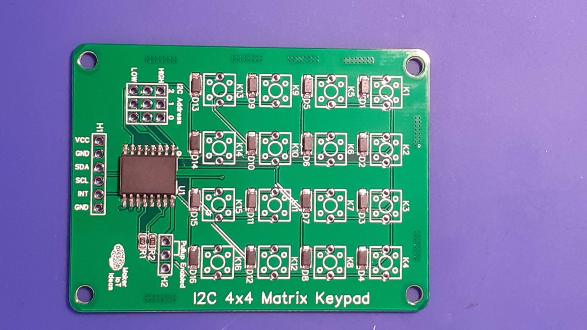
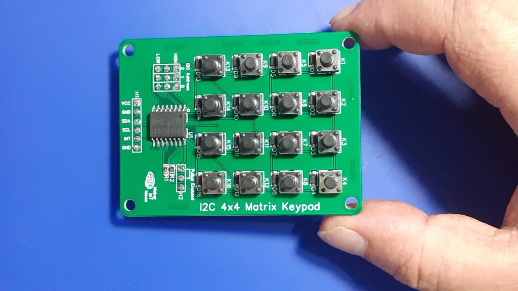
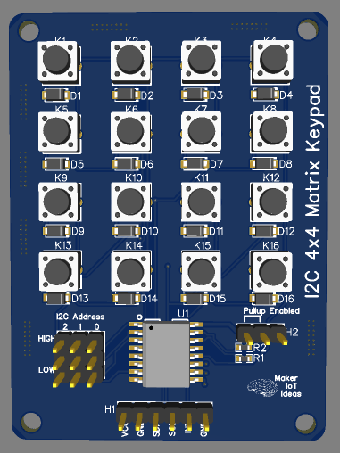
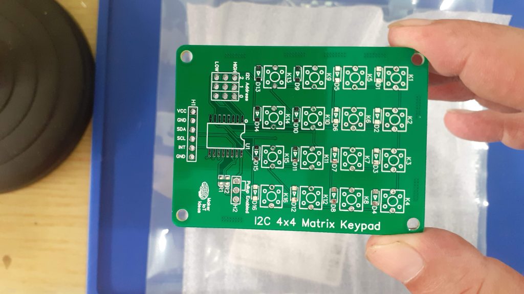
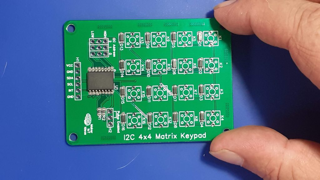
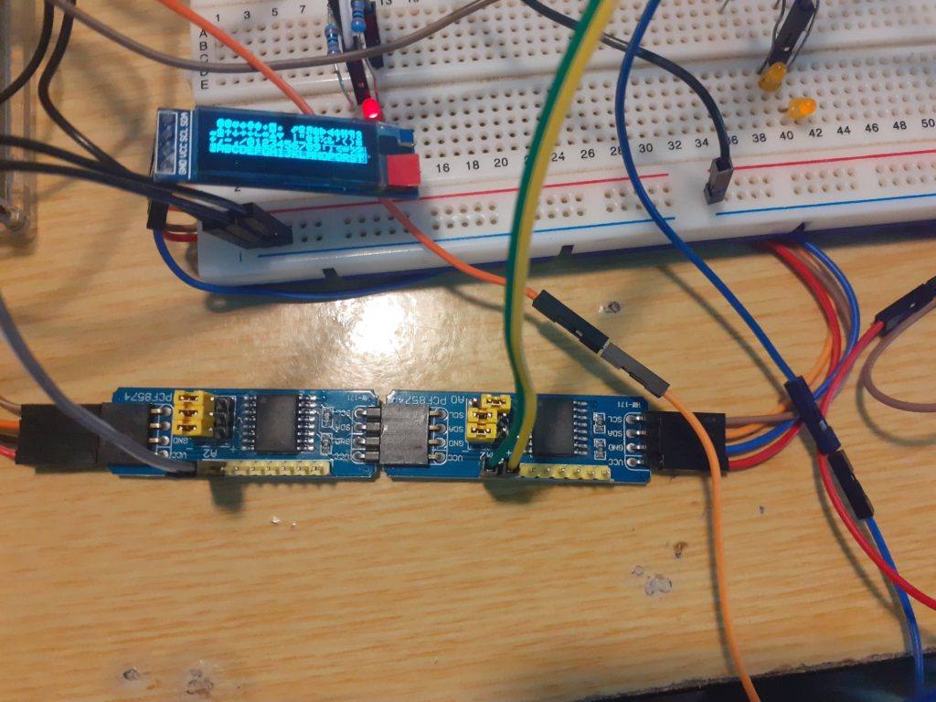
1x Matrix Keypad (4×4) Controlled via an PCF8574 IO expander with selectable addressing.
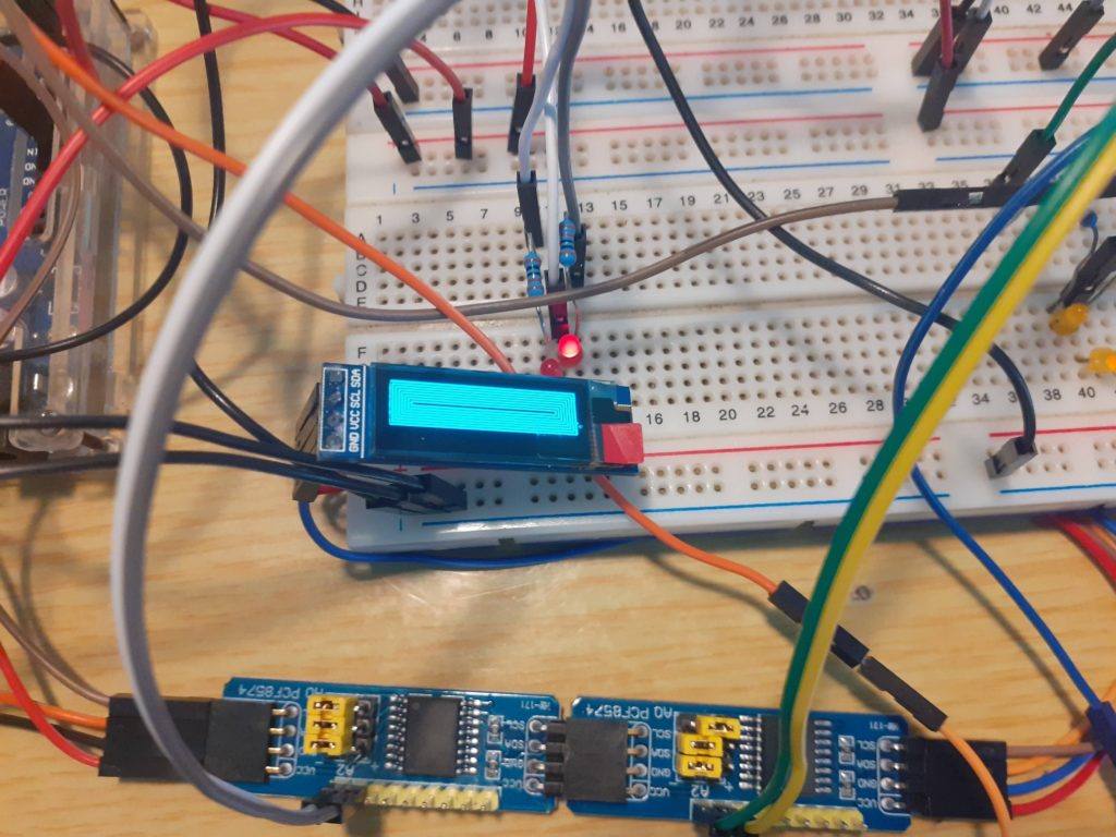
1x SSD1306 OLED I2C Display
4x Momentary pushbuttons, configured to be used with internal pullups – i.e pushing the button pulls the GPIO LOW
2x Rotary Encoders, with integrated Pushbutton, also configured as Active LOW
The board has all of the connectors and jumpers on the back, making it possible to mount it to an enclosure as a control panel.
I have also provided an additional I2C header to make it possible to add additional devices to the I2C bus easily
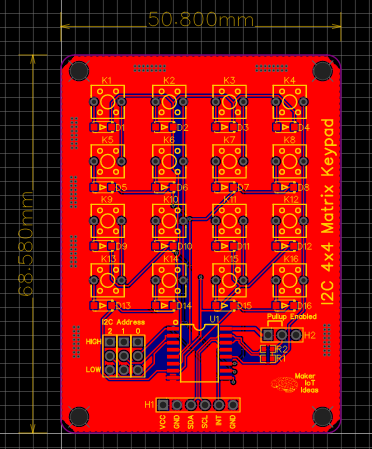
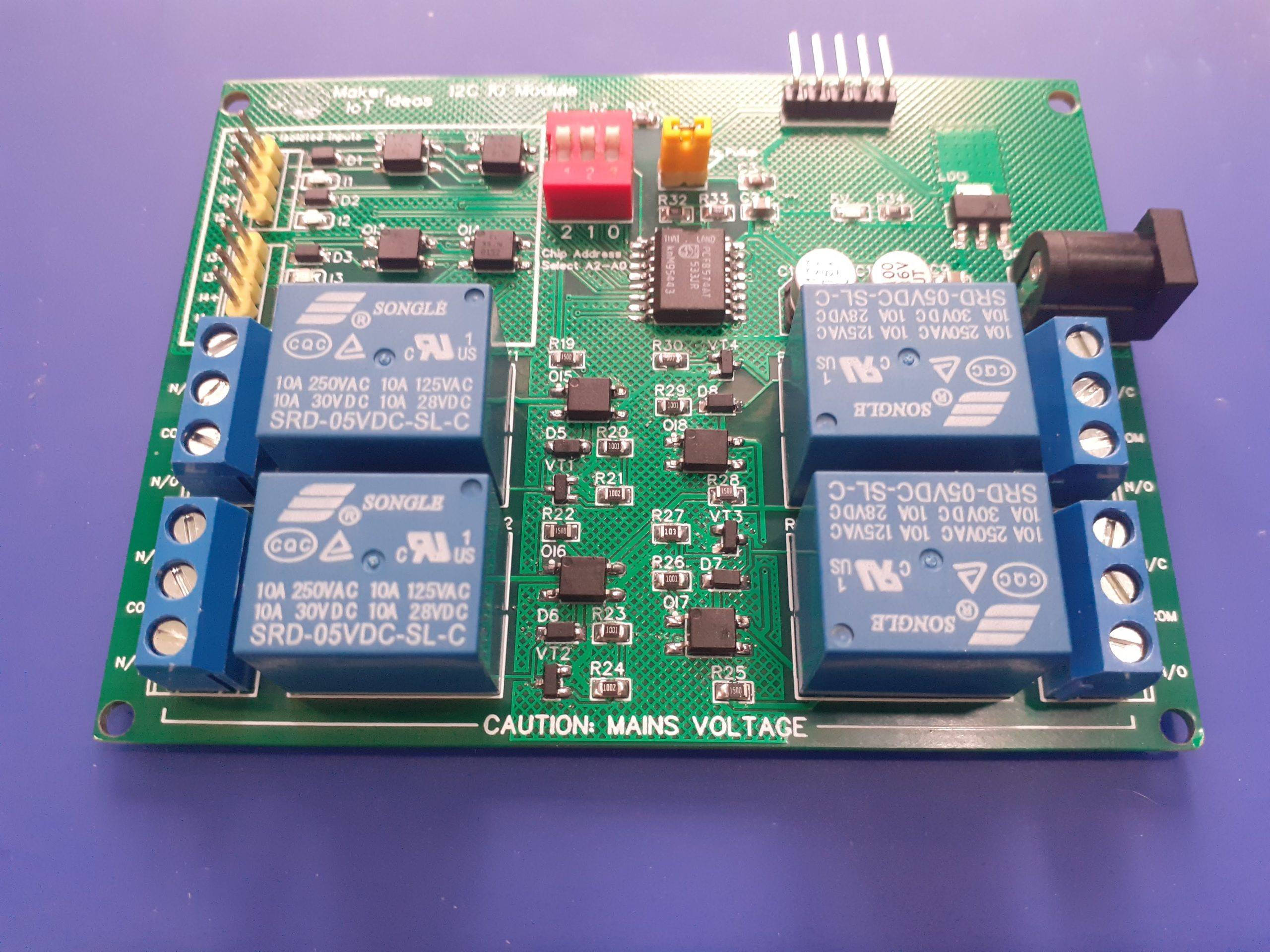
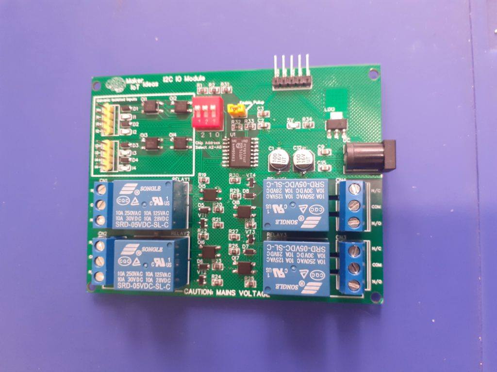
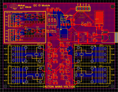
The PCB in Detail

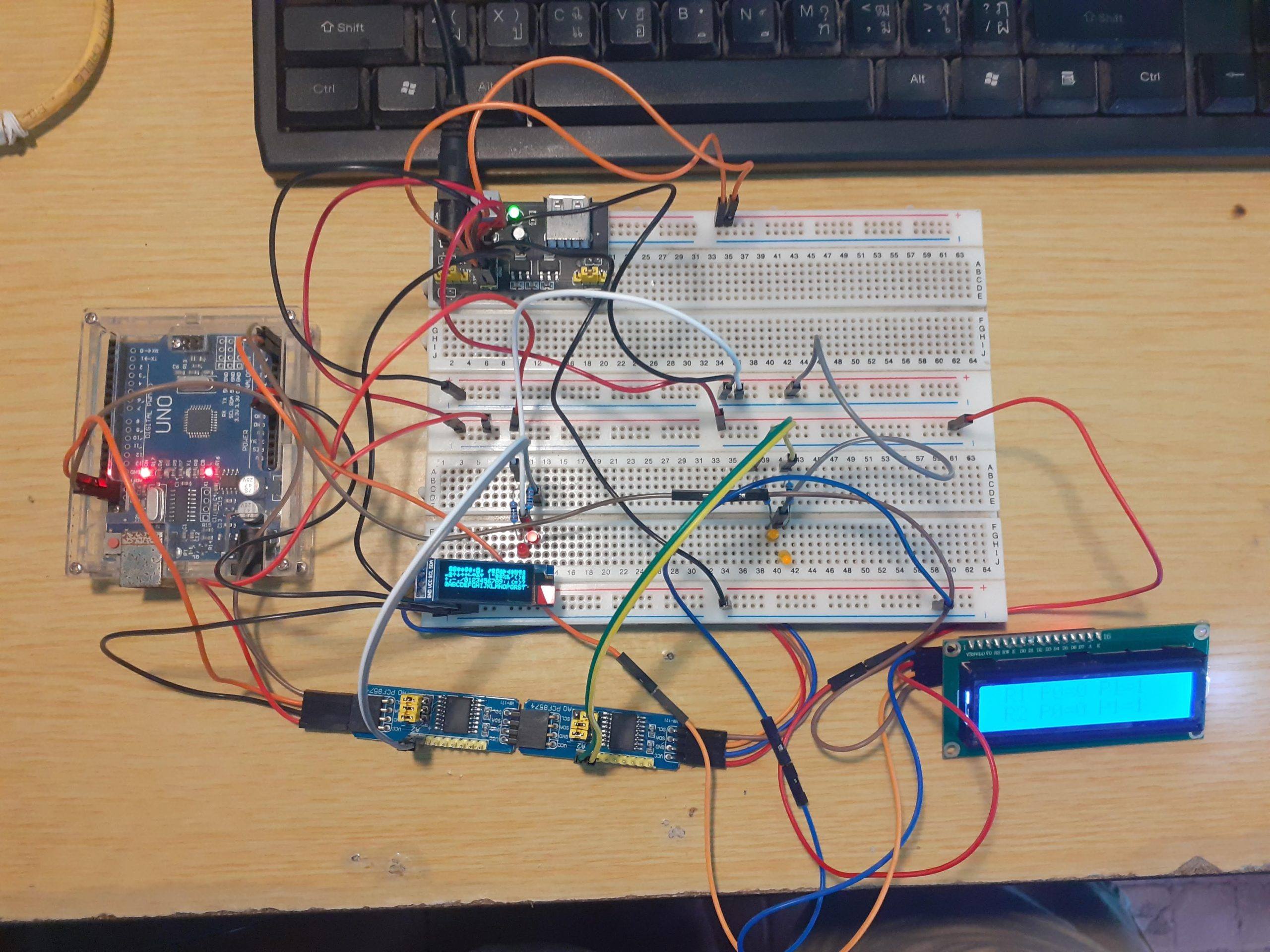
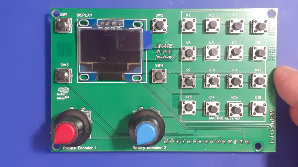
Starting from left to right, we have two push-buttons, an OLED display, with two rotary encoders below the display, and another two momentary push buttons. On the Right, we have a 4×4 matrix keypad, and various pin headers for connection to a microcontroller of your choice.

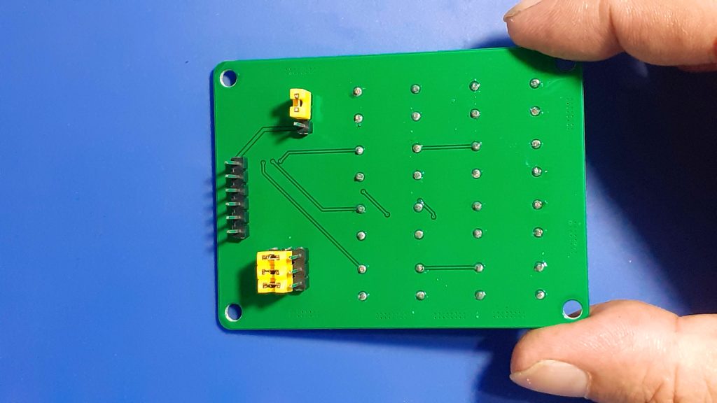
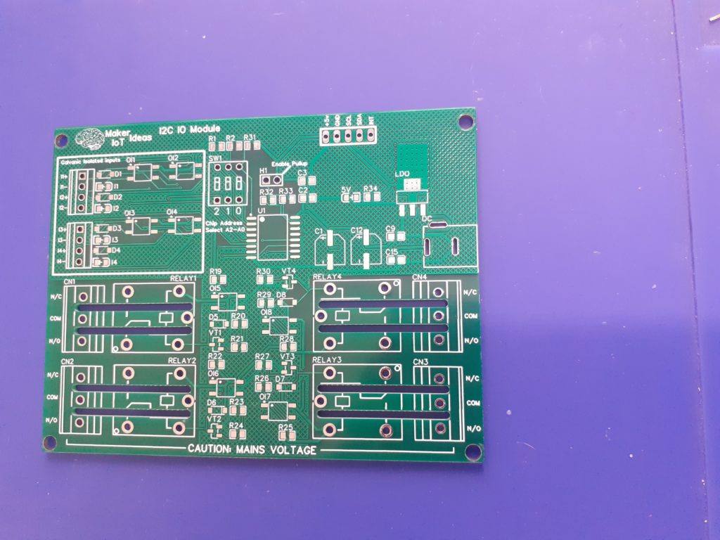
On the back, we have the PCF8574 IO expander for the Matric keypad, addressing Jumpers for the IO expander, as well as the two pin headers for connections to and from a microcontroller…
The Pinouts of these are as follows:
Horizontal 15 pin 2.54mm connector
SDA I2C Data
SCA I2C Clock
GND
SW4 Momentary Push Button 4
SW3 Momentary Push Button 3
SW2 Momentary Push Button 2
SW1 Momentary Push Button 1
RE2-D Rotary Encoder 2 Push Button
RE2-B Rotary Encoder 2 Pin B
RE2-A Rotary Encoder 2 Pin A
RE1-D Rotary Encoder 1 Push Button
RE1-B Rotary Encoder 1 Pin B
RE1-A Rotary Encoder 1 Pin A
GND
VCC 3.3v to 5v DC
The Expansion header extends the I2C Bus, as well as proved access to the interrupt pin on the PCF8574. VCC and GND are also provided.
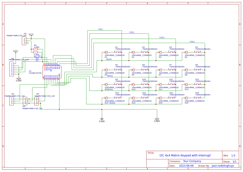
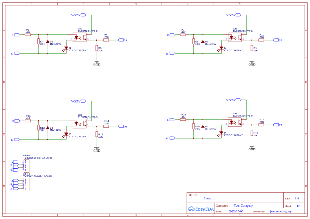
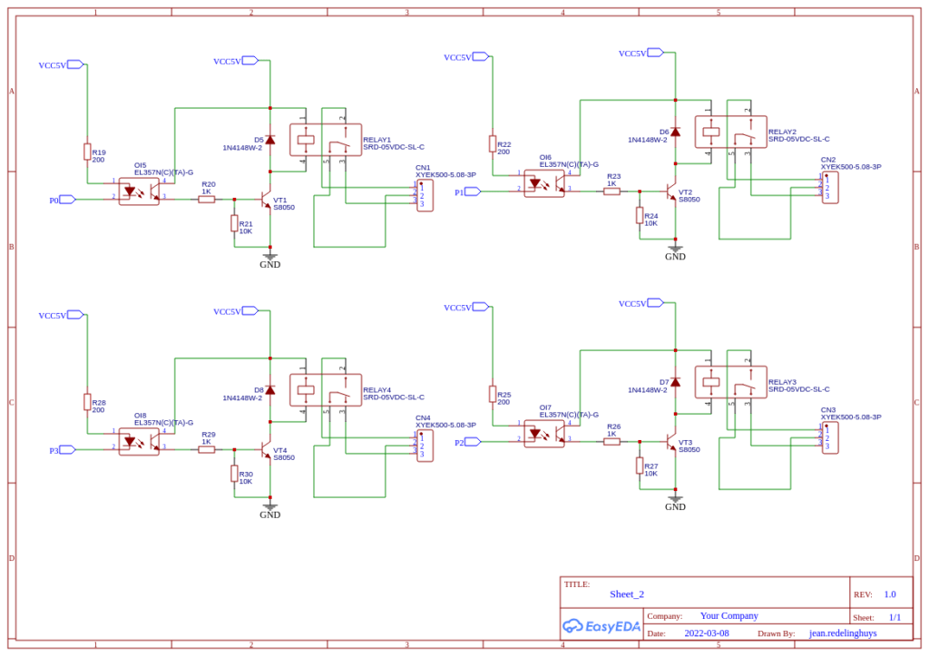
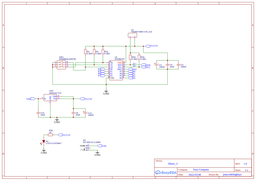
The Schematic

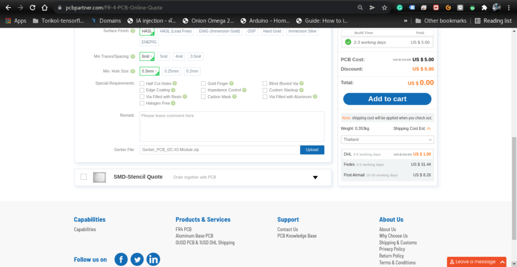
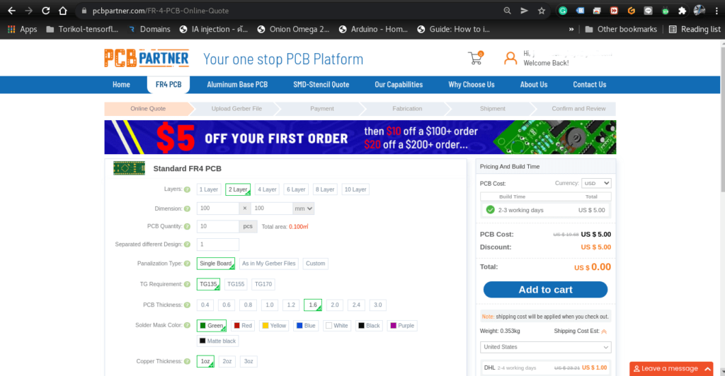
Manufacturing the PCB
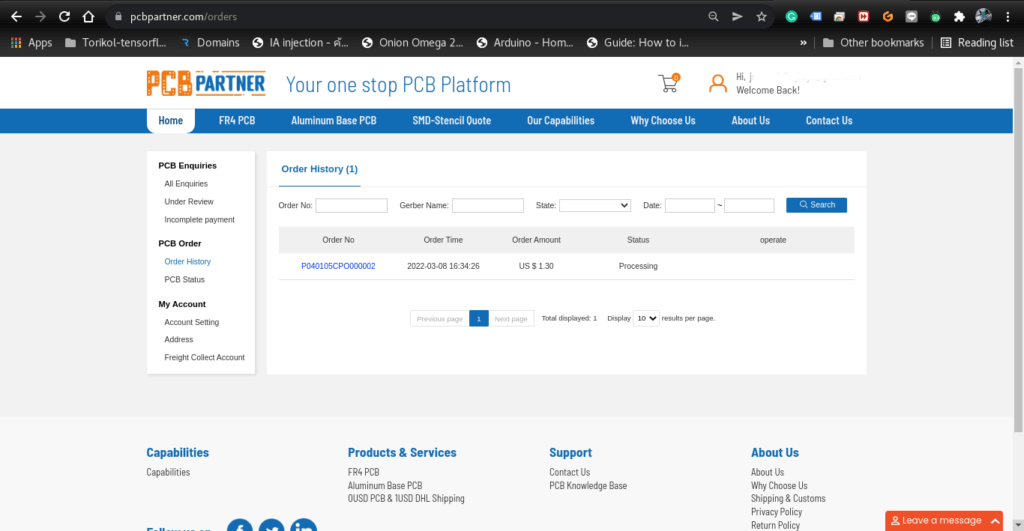
I choose PCBWay for my PCB manufacturing. Why? What makes them different from the rest?
PCBWay‘s business goal is to be the most professional PCB manufacturer for prototyping and low-volume production work in the world. With more than a decade in the business, they are committed to meeting the needs of their customers from different industries in terms of quality, delivery, cost-effectiveness and any other demanding requests. As one of the most experienced PCB manufacturers and SMT Assemblers in China, they pride themselves to be our (the Makers) best business partners, as well as good friends in every aspect of our PCB manufacturing needs. They strive to make our R&D work easy and hassle-free.
How do they do that?
PCBWay is NOT a broker. That means that they do all manufacturing and assembly themselves, cutting out all the middlemen, and saving us money.
PCBWay’s online quoting system gives a very detailed and accurate picture of all costs upfront, including components and assembly costs. This saves a lot of time and hassle.
PCBWay gives you one-on-one customer support, that answers you in 5 minutes ( from the Website chat ), or by email within a few hours ( from your personal account manager). Issues are really resolved very quickly, not that there are many anyway, but, as we are all human, it is nice to know that when a gremlin rears its head, you have someone to talk to that will do his/her best to resolve your issue as soon as possible.
Find out more here

Assembly and Testing
The assembly of this PCB was relatively easy, as it contains only a single SMD component. I do however have to alert you to a certain caveat…
On the PCB, the I2C OLED display pinout is, from left to right,
VCC GND SDC SDA
I have however come across similar displays that swap the GND and VCC pins… and some that even have SCL and SDA swapped…
It is thus quite important that you check your display BEFORE soldering it to this PCB…
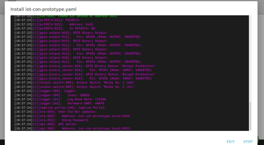
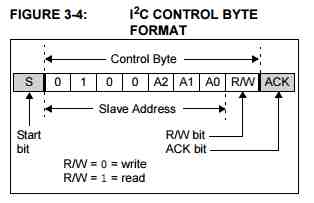
Addressing the PCF8574 is also quite easy, with the jumper towards the top is a high, and towards the bottom is a low… They are marked A2 A1 A0 and thus, counting in binary, all low will be 0x20h and all high will be ox27h
Also, note that there are NO I2C Pullup resistors on the board. My microcontroller PCB’s usually have these already, and most I2C Sensors, including the OLED Display that we use, already include as well…
You should thus check what you have on your own hardware, as it is quite impossible to cater for every situation… In a future version, I may add selectable pullup resistors onto this board as well…
Coding and Firmware
The possible uses of this board is quite broad, and the code possibilities are thus also quite extensive. Since I mainly use ESPHome or the Arduino IDE with most of my projects, I wont be including any specialised code here. I think it is enough to say that almost all of the available PCF8574 Matrix Keypad libraries available for the Arduino IDE will fork with this board…
The pinouts are important, and thus :
Row 0 – P0
Row 1 – P1
Row 2 – P2
Row 4 – P3
Col 0 – P7
Col 1 – P6
Col 2 – P5
Col 3 – P4
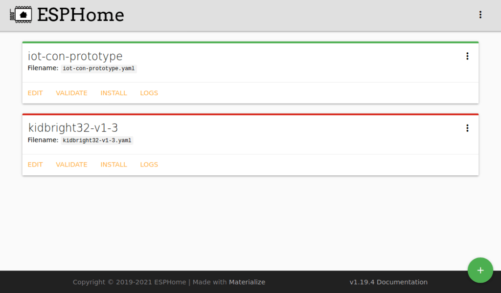
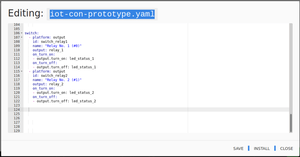
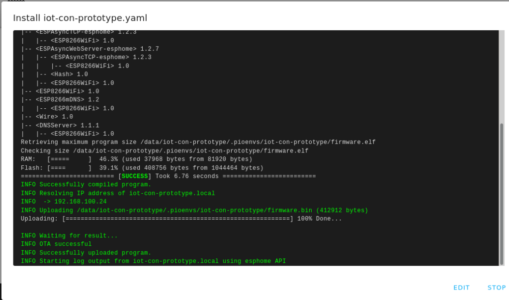
As far as ESPHome goes, you will need to
1) Add an I2c bus for your device
2)Add a PCF8574 component
3)Add a Matrix Keypad component, and refer the rows and columns to the pins on the PCF8574 – See below for an example of how I have done that in a previous project.
#I2C bus

i2c:

sda: 4

scl: 5

scan: true

id: I2C_Bus

#
# In my case, SDA is on GPIO4 and SCL is on GPIO5
# This is similar to the standard configuration on a NodeMCU v2 Dev board
#

#
# The next step is to configure the actual IO Expander, which in my case is located
# at address 0x27
#

#PCF8574

pcf8574:

- id: 'pcf8574_hub'

address: 0x27

pcf8575: false


#
# Now we can add the actual keypad interface to the YAML file
# Take note of the difference from the ESP32 file above.
#
#

#KEYPAD

matrix_keypad:

id: mykeypad

rows:

- pin:

pcf8574: pcf8574_hub

# Use pin number 0

number: 0

# In the ESP32 file, we wHereould specify a pin directly like:
#
# -pin: 17
#
# That approach will not work for us.
# The reason for that is that we have to redirect the GPIO to a
# physical pin on the PCF8574 IO expander.
#
# That is done with the following syntax
#
# - pin:
#pcf8574: pcf8574_hub -- This is the ID of the PCF8574 device -
#number: 0 -- The actual pin number

- pin:

pcf8574: pcf8574_hub

# Use pin number 0

number: 1

- pin:

pcf8574: pcf8574_hub

# Use pin number 0

number: 2

- pin:

pcf8574: pcf8574_hub

# Use pin number 0

number: 3

columns:

- pin:

pcf8574: pcf8574_hub

# Use pin number 0

number: 7

- pin:

pcf8574: pcf8574_hub

# Use pin number 0

number: 6

- pin:

pcf8574: pcf8574_hub

# Use pin number 0

number: 5

- pin:

pcf8574: pcf8574_hub

# Use pin number 0

number: 4

keys: "123A456B789C*0#D"

has_diodes: false
The Rotary encoders and momentary push-buttons can be handled in the same manner, using standard libraries in the Arduino IDE, or a rotary encoder component in ESPHome…
The OLED display would also be handled as above, with a DISPLAY component in ESPHome…
Summary and next steps
The next steps, for me at least, would be to design and CNC cut a suitable enclosure for the IO panel/Control panel in order to make it easier to use…
The panel was designed to be a tool to aid me while designing, and part of my never-ending battle getting rid of breadboards.
It does its job well, at least so far, and works as I have intended it to.