

MakerIot2020.com is usually about my creations, or at least my attempts to create something. Today we shall change that, and publish a Review of the Elecrow Crowpanel PICO HMI 4.3″ Display.
While I usually do not do any sponsored reviews of products, I decided to make an exception in this case. Why? Well, when I received the product documentation for this module from Elecrow, I was immediately interested, since the module fit in perfectly with a project that I was working on, and while it was quite obvious that there would be a huge learning curve involved, with many hours spent chasing documentation and other resources, I believed that the potential functionality and thus gain for my project would make all of this worth-while.
What is this module exactly?
CrowPanel Pico Display is an HMI module series that utilizes the powerful Raspberry Pi RP2040 (ARM Cortex-M0+) as its main controller. It is equipped with a 32-bit dual-core chip running at a clock frequency of up to 133 MHz. With 264kb of built-in SRAM and a 2MB flash memory chip, it integrates power supply, voltage regulation, and counter functions into a single microcontroller. This series of touch screens incorporate high performance, low cost, and user-friendly features.
The Pico 4.3” Display has a 320*240 resolution and capacitive touch for more sensitive control. It has flexible I/O peripherals and a unique programmable input/output (PIO) subsystem, including practical communication interfaces such as I2C, UART, common IO ports, and USB. It also has a built-in BW16 wireless network module, dual-band Wi-Fi (2.4GHz or 5GHz) + low-power Bluetooth 5.0, supports remote monitoring and network management functions, and easily accesses IoT devices and systems. It is also equipped with functions such as a lithium battery interface and a buzzer alarm and can communicate with almost any external device, providing professional users with excellent flexibility and scalability, and achieving seamless connection with the physical world and smart home control.
The module comes with abundant resources, including development SDK, and documentation. It has a very low entry barrier, making it suitable for beginners and hobbyist users. It not only can use Arduino IDE and CircuitPython to program, but also supports the LVGL graphics library and Squareline Studio to customize the desired UI interface. It serves as an excellent platform for machine learning applications and is the preferred solution for Pico-like HMI interaction terminals.
- 4.3 inch Pico Display: 320*240 resolution, IPS Panel, capacitive touch and support multi-touch
- RP2040 Microcontroller: Equipped with a 32-bit dual-core chip, it achieves a maximum clock frequency of 133 MHz.
- Wireless connection: Support 4GHz IEEE 802.11b/g/n and 5GHz spectrum range, support Bluetooth 5.0 and BLE
- Energy Efficiency: Supports low-power sleep and hibernation modes, promoting energy conservation and environmental consciousness.
- Exceptional Extensibility: A wealth of interfaces, including I2C, UART, IO ports, USB, a lithium battery interface, and a buzzer alarm, ensures remarkable extensibility.
- Ease of Use: A user-friendly experience is guaranteed with the provision of a detailed development SDK, and comprehensive documentation, ensuring a smooth learning curve.
Specification
- Main Chip: RP2040
- Processor: Dual-core 32-bit ARM Cortex-M0+ @ 133MHz
- Memory: 264kB on-chip SRAM (supports up to 16MB of off-chip flash memory)
- Screen Size: 4.3 inch
- Resolution: 320*240
- Signal Interface: SPI
- Touch Type: Capacitive Touch
- Panel Type: IPS
- Power Input: 5V-2A
- Active Area: 95.04*53.856mm(W * H)
- Dimensions: 124.7 * 76 * 14.2mm(W * H * D)
Unboxing and initial thoughts
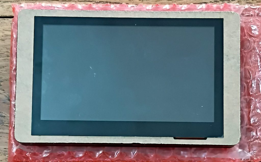
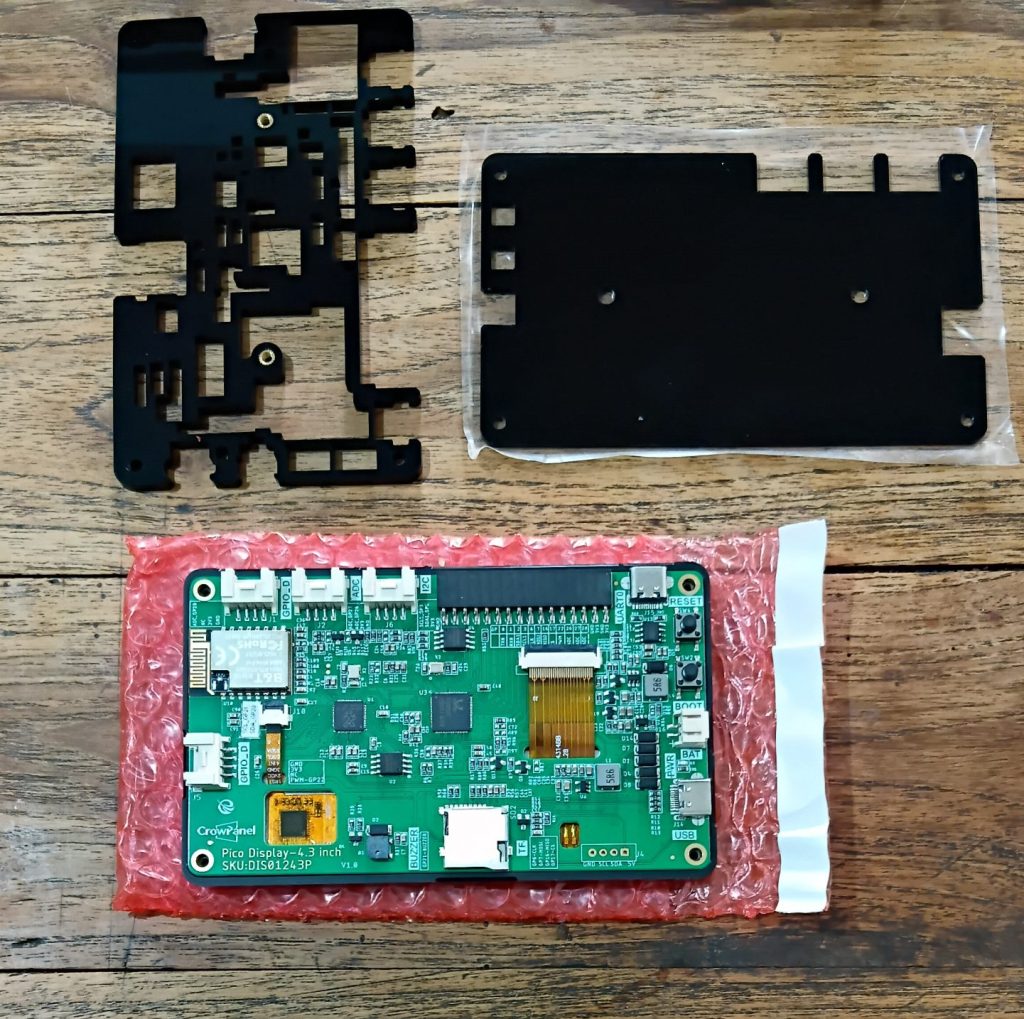
The display module came very well packaged.
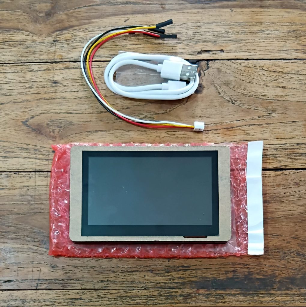
and includes the display module, a USB-C programming cable and a single 4 way io cable
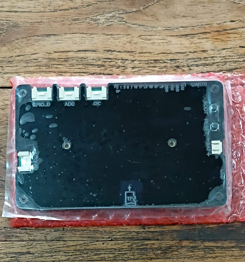
All the GPIO breakout headers, as well as the Reset and Boot buttons are located on the back of the module. This may be a double edged sword though, as I am still unable to find a way to gain access to these pins without the buttons, while soldering wires directly to them is definitely possible, I really don’t want to do that. Access to these buttons are quite essential, as they are needed to program the device, and once mounted into an enclosure, access to them will be quite difficult, without completely disassembling the enclosure. Time will however tell if this is really a problem or not.
Dissasembly – Looking at the stuff inside
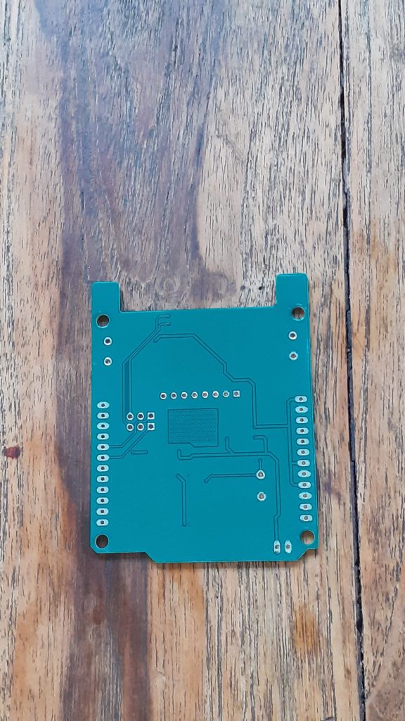
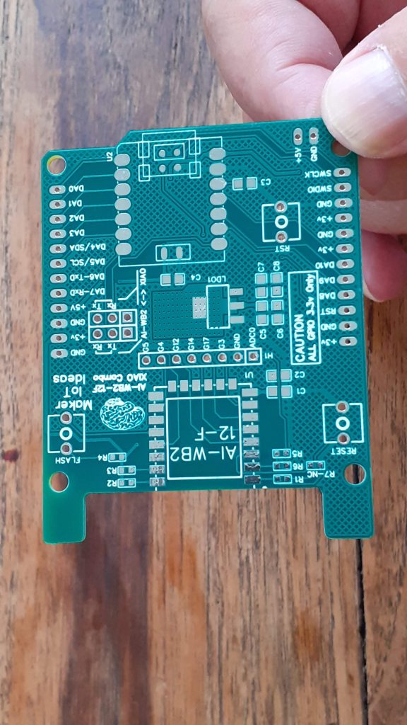
I disassembled the unit because we must look at what is inside – otherwise, we would not be makers, would we? The quality of the PCB seems to be very high, with detailed silkscreen legends everywhere.
Let us take a closer look at a closeup
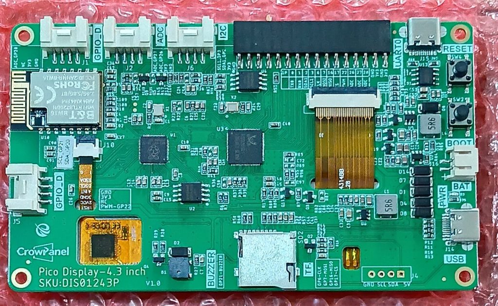
From what I can see, everything seems well organised, with all relevant circuitry in blocks. The Wifi and Bluetooth module is correctly placed on the right-hand edge of the board, ensuring that we shall have no issues with signal strength, also note that the antenna area is free of tracks and copper pours.
My initial thoughts – about the hardware
The PCB seems to be of very high quality, and the layout of the board clearly required a lot of thought. The unit has a very solid “feel” to it.
However, I do not like the choice of gpio connectors on the board. Screw-type terminals may have been better, at least in my opinion. The Reset and Boot buttons, as previously mentioned are at the back of the board, this may present issues if the panel is mounted into an enclosure. Additional header pins, to enable the installation of external buttons would maybe have been a good idea – time shall however tell if this is really a problem or not.
Supplying power to the board is another issue. Using a USB-C connector is in my view appropriate for bench use. Installing and using this module in a “real-life environment” would require a different type of connector, like a screw-terminal type, that would make it easy to connect power to the unit from more types of power supply units – I am specifically thinking of using it in an Automotive environment, where USB ports are not necessarily always available
Gui Generation – the LVGL graphics library and Squareline Studio
Squareline Studio seems quite sufficient to generate basic GUIs for the display module. The interface is relatively easy to use, and the widgets available is sufficient for a functional, although fairly basic GUI interface. It is possible to code directly in LVGL and add any advanced or customised widgets that way – although this should be done directly in your programming IDE of choice.
It is possible to export your generated GUI directly to Arduino code, and from there make changes to get things working – but with a few very important caveats.
1) It seems that SquareLine Studio suffers from version creep, with new versions popping up in incredibly short timeframes. This means that the latest version does not generate all the required Arduino files anymore – the main .ino file seems to always be missing, with only .c and .h files being generated.
This makes it necessary to perform a few extra steps to get things going ie.
– Copy the example project from Elecrow into a folder – this includes a .ino file
– Remove example Gui related files
– Rename the .Ino to <xxxxxx>.ino (as required by your project )
– export the GUI code into this folder
– edit the .ino file to include you custom code etc…
This results in a successful upload to the board, with a fully functioning Gui… but is a bit of a roundabout way to get things done. Let us see what happens in the future, maybe this will be repaired in future?
Documentation and other Resources
Elecrow has made a lot of written documentation available on their website, here. There are links to all the different RP2040-based Crowpanel modules.
It is however VERY VERY important to note that some of the documentation presented here seems to be incomplete, especially the 4.3″ display module, which uses a completely different display driver than the other members of the RP2040 Crowpanel devices…
I would thus recommend that potential users take a VERY close and detailed look at Elecrow’s YouTube tutorial on these boards, available here. These videos
highlight all the differences, and gets you up and running in a few minutes – with the unfortunate issue of using video to teach technical things – you will have to pause and continue quite a few times… It is however completely worth it in the end, as the information presented is perfect, and invaluable to get started with this module…
Pinout

| Pin Name | Description | Connect Type |
|---|---|---|
| PWR | Power LED. | |
| RST | Reset button. Press it to reset the system. | |
| BOOT | Hold the BOOT button and press RST button to make the RP2040 enter flash mode. | |
| TF | Provide offline save and extra storage space. | |
| UART0 | Build the communication among Logic modules, including serial communication module and print module. | |
| GPIO_D | Connect with external hardware devices to realize communication, control, or data acquisition with external devices. | HY2.0-4P |
| I2C | Connecting microcontrollers and other peripheral devices. | HY2.0-4P |
| BAT | Connect with the lithium battery. Connect USB-C port to charge the battery. | PH2.0-2P |
| ADC | By analyzing and processing the input signal, the control system can realize the precise control of the controlled object. | HY2.0-4P |
| PICO 4.3-inch HMI Port | Pin Number |
|---|---|
| I2C | GP2(SDA), GP3(SCL) |
| UART0 | RX(GP1); TX(GP0) |
| UART1 | RX(GP5); TX(GP4) |
| GPIO Pins | GP0~GP3, GP6,GP7, GP16,GP17,GP22,GP26~28 |
| ADC | GP26(SDA),GP27(SCL) |
Conclusion – and next steps – for me at least
I am pleasantly surprised with this module. yes, the learning curve is steep, and there are a few very uncomfortable runarounds that has to be performed to use Squareline Studio together with the Arduino IDE to generate GUIs for the module.
We do however have to remember that Squareline Studio and Elecrow are two different companies. The GUI generator has to cater for many different hardware devices. It would thus be unfair to say that the Elecrow Crowpanel module has a problem, just because Squareline Studio requires you to jump through a few hoops to get things working with the Arduino IDE.
I am thus giving the module a thumbs-up and saying all is good. However, I would like to see some improvements in connectors, especially for powering the device, as well as connecting a battery to it, screw-terminals would be much more convenient.
Externally accessible headers for at least the Reset button would also be a very good idea.
Performance-wise, I received a 16mb flash version from Elecrow, and it is snappy, to say the least… the graphics are well-defined and clear, and the touch interface is very responsive.
As mentioned before, the learning curve is steep. This is not a device that you can pick up and start running within a few minutes – You will have to invest some time to get familiar with it – believe me, it will be worth all of that effort!
As for my future projects, I am currently busy interfacing the 4.3″ Crowpanel HIM module with one of my custom PCB projects and will report back more on that once the project is completed.


