An Easy RP2040 Logic Analyzer Shield – Scoppy Scope Part 2

Scoppy Scope Logic analyser Shield with Logic Probes

As part two out of a series of three articles (part 1), This is the Scoppy RP2040 Logic analyzer shield, for use with our Raspberry Pi Pico Carrier board and the Scoppy Oscilloscope firmware for the RP2040.

In Part one, we took a very quick look at the installation of the firmware, as well as the basic limitations for use of this very useful project.

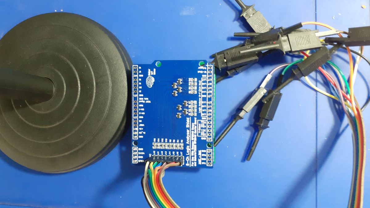
In this part, I want to take a quick look at my Logic Analyser shield, for use with this project, as well as the Raspberry Pi Pico Carrier Board. In part one, we saw that the logic analyzer inputs are limited to 3.3v by the RP2040 GPIO pins. This shield is a prototype attempt to overcome those limitations by using logic-level conversion.

What is on the PCB ?

The PCB is designed to be an add-on shield for the Makeriot2020 Raspberry Pi Pico Carrier Board. (Get your own here) It is in the same form factor as the Arduino Uno shields, but with pinputs specific to the RP2040 and Raspberry Pi Pico.

8 Ch Logic analyser Shield for use with Scoppy and MakerIOT2020 Pico Carrier Board

All Raspberry Pi Pico pins are broken out and labelled, as well as all of the pins specific to the Scoppy App have been clearly labelled. The board are stackable onto the Pico Carrier board, via standard 2.54mm Male Headers, or extra long, stackable female 2.45mm headers, similar to those found on common Arduino shields.

The use of stackable headers will allow simultaneous use of the logic analyser shield and the Analog frontend shield, introduced in part 3 of this series.

In addition to that, a 2×8-way 2.54mm Male header provides access to the 8 logic converted logic analyser inputs.

Logic conversion is done with a simple circuit, comprising a Bss138 N-Channel Mosfet and two 10K resistors per channel.

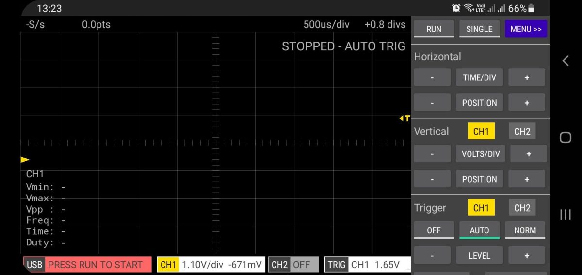
The shield is powered directly from the Pico Carrier board, which is in turn powered from the OTG cable to the Android Phone or tablet used to display the captured data. ( see Part 1 for installation instructions and other details regarding the Scoppy Project)

The logic level converters allow the use of a 5v logic signal, which is an improvement over the original design, which allowed only 3.3v inputs.

The Schematic and PCB Layout

Logic analyser shield schematic


PCB Layout

Manufacturing

The PCB for this project has been manufactured at PCBWay.
Please consider supporting them if you would like your own copy of this PCB, or if you have any PCB of your own that you need to have manufactured.

PCBWay

Some more pictures of the device

Installation instructions (repeated from Part 1)

Scoppy Scope Installation

All credits for the development of the Scoppy firmware goes to fhdm-dev. This shield is a modification made by MakerIOT2020, and thus belongs to me. In the spirit of the original project, It will however be released to the public as a free open-source project ( free as in free download, free schematic, free design ). The PCB manufacturing files will be made available for free at a later stage, or can be ordered from PCBWay from this link

RP2040 Oscilloscope and Logic Analyser

Oscilloscopes and Logic analysers are essential instruments for every serious electronics hobbyist. They are however quite expensive, and thus beyond the reach of many people starting out with electronics. Today, I will show you a cheap solution, an RP2040 Oscilloscope and Logic analyser…

Before we get started, we need to clear up a few things first:
1). This is not my own project. It was designed and built by someone else.
2). This is not a professional grade Oscilloscope or Logic analyser
3). The range of input voltages, as well as the frequencies that you can measure, are limited.

What is this, and why do I bother with it?

This post is about the Scoppy Occiloscope Firmware, designed by fhdm-dev. I have no affiliation with him/her, I came across this recently and found it useful in the sense that it may help others gain access to instrumentation to greatly help them with electronics.

I did design some derived pcb components that works with this project, in order to take care of some limitations that I saw in the original project. More on that in two follow-up posts, in which I will show you two PCB’s that I designed to use with this project, and analog Frontend ( based on a public design by fhdm-dev, as well as a Logic analyser shield, of my own design

before we do this, we need to look at the basic Scoppy design and its firmware.

Getting Started

You will need a few things to make use of this project, the most important will be the Scoppy App ( available from the Google Playstore ), and an Android Phone.
You will also need a USB OTG Cable/hub for the phone, as well as a Raspberry Pi Pico or Pico W

The Installation and Getting Started Guide is very well documented, and as such, I will not spend a lot of time on that.

My own Setup

I have decided to use my own Raspberry Pi Pico Carrier board for this project, as it will allow me to get away from the breadboard, as well as serve as a platform for easily expanding on the project via expansion shields, as you will see in later articles.

Makeriot2020 Raspberry Pi Pico Carrier Board

This PCB, in Arduino Uno form Factor, will make putting the entire project into a case quite easy, as well as hopefully keep the number of floating hookup wires to a minimum. ( hopefully reducing some notice and other stray signals from interfering too much with our signals)

After installing the application, which is quite easy, we need to load the firmware onto the RP2040. This is also extremely easy is you follow the guide at the top.

Please note that the Android app has two modes, a freeware mode, limited to one channel, and a paid version, with no limitations. I recommend that you consider buying the paid version, as it only costs a few dollars ( I paid $USD2), and will motivate the developer to keep working on the project, and improving it.

Scoppy Application, Main Interface – Oscilloscope
Scoppy Menu
Scoppy Logic Analyser Screen

As we can see, the interface is quite clean, and easy to use.

What are the limitations?

There are quite a few limitations, namely frequency and voltage input.
From what I can understand, the frequency limit seems to be around 25Khz, with the voltage level limit being 0.0v to 3.3v ( as per the limit of the RP2040 ADC

Please make sure that you follow all instructions on the original page, as you can very easily damage your Android device as well as the Pico if you apply a voltage outside of the allowed range.

On the logic analyser side, It is also important to note that you should stay in the 0.0v to 3.3v range of the Pico GPIO’s.

While these limited ranges will definitely limit what you can do and measure, It will still be a very useful project. In the next part of this article, I will show you how I have solved the logic analyser voltage range issue… Allowing you to analyse 5v signals as well.