A Soft Start Circuit Experiment

Every single project that we build needs an On/Off switch. Hardware switches are big and clumsy and can be quite expensive. Most of them also don’t look very good.

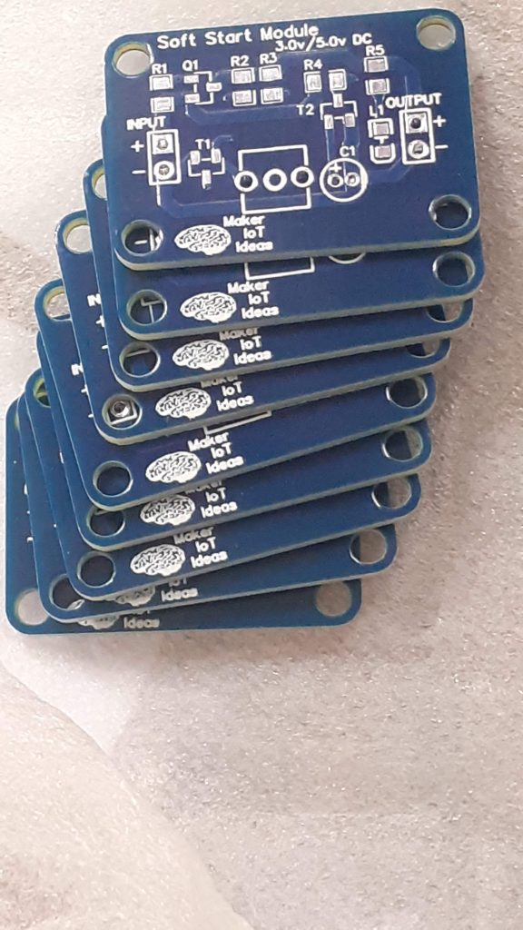
This post will be about an experiment that I recently performed, building a reliable soft start circuit, or latching circuit.

Full disclosure: I did not design this circuit. Full credit to the designer, who shall be mentioned later.

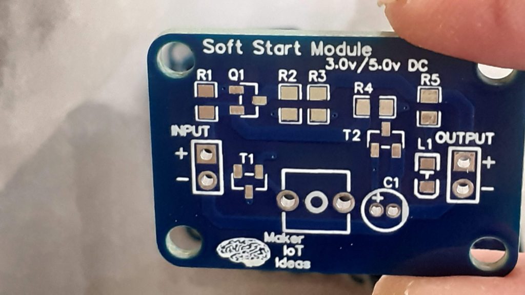
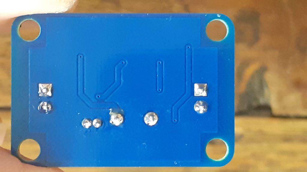
As such, This shall be about my experiences with this great little circuit, and also to show off the neat little prototype PCB that I designed and had manufactured for this experiment. It only took a few minutes to design, and even less to assemble.
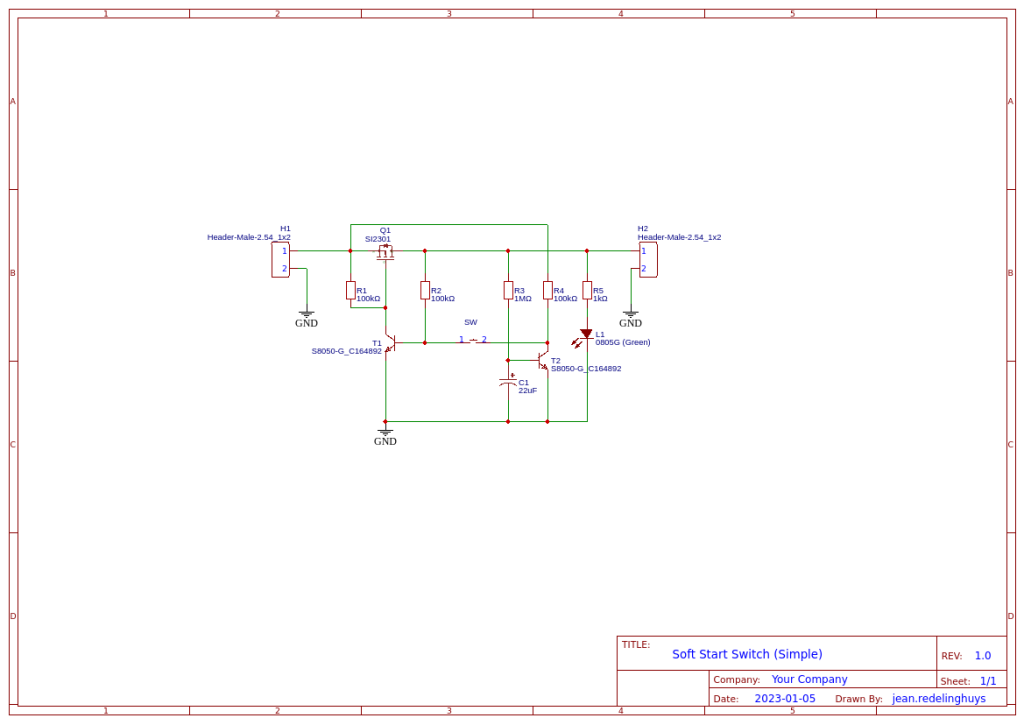
The Schematic

Schematic

How does it work?

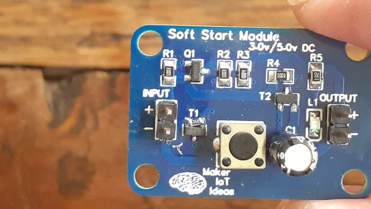
To answer this, let us look at what components are in the circuit first.
Q1 is a P-Channel Mosfet. I chose the SI2301, because that is what I had lying around.
T1 and T2 are NPN BJT transistors, I chose S8050’s here, and also tested 2n2222a’s with great success.
Other components are 3 100k pullup resistors, 1 1M pullup and an 1k dropper resistor for the indicator LED.

In the off state, R1 (100k) keeps the gate of Q1 tied to the supply voltage, thus keeping the MOSFET switched off.
T1’s collector, also connected to the MOSFET Gate, are thus pulled High, with the Base of T1, although pulled High, connected to the Drain of Q1.

Q1 is still off, so that base will be low, for now at least.

The collector of T2, is pulled up to the supply voltage via R4, and also, through the push button, to the base of T1.

The base of T2, is pulled up via a 1M resistor to the drain of Q1, and a 22uf to 47uf electrolytic capacitor to ground.

The emitters of both T1 and T2 are grounded.

When you press the switch, the base of T1 goes high, and this switches T1 on, pulling the gate of Q1 to ground, switching it on. This now pulls the base of T1 high through R2, latching it on, and keeping Q1 switched on. This also pulls the base of T2 high through R3. As T2 is now also switched on, the junction between the collector of T2 and the switch is now for all purposes a ground.

Now, when you push the switch again, the base of T1 is pulled down to ground via T2. This switched off Q1. As the capacitor on the base of T2 can now discharge, the circuit is reset, and the next press of the switch will turn it on again.

How big a load can be switched?

Obviously this depends on the rating of the MOSFET at Q1. In my experiments, a load of about 150mA was easily controlled, but more than that, started to somehow drain the cap at C1 too fast, and the circuit would reset.

This is not a problem to me, as the circuit is ideal to switch a relay, which in return can switch the main load.

What other issues did I encounter?

The SI2301 seems to have a small amount of leakage, which allowed a few millivolts to activate T1 or T2. I solved that with the addition of a 10k pulldown to ground, on the base of T1.

This does not seem to be the case with other MOSFETS, and I believe changing the value of R1 to provide a stronger pullup, might solve this issue.

Where does the circuit come from?

I found the circuit, and explanation on the excellent Youtube channel EEVBlog.
The owner, Dave, does an excellent job of explaining how this works. All credit to Dave for this excellent circuit!

It has zero current consumption in the off-state, and very little when on.

Manufacturing

The PCB for this project has been manufactured at PCBWay.
Please consider supporting them if you would like your own copy of this PCB, or if you have any PCB of your own that you need to have manufactured.

PCBWay

Conclusion

I believe this is a great little circuit to keep around, with many excellent use scenarios. It does need a bit of fiddling to get to work perfectly every time ( as you can use many different P Channel Mosfets and NPN BJT transistors)

It provides an excellent alternative to a mechanical switch, and for my own use, the PCB Module is small enough to be mounted into an enclosure with another project with ease.

8Ch NMOS Breakout Module

As a companion module to my recently published 8Ch PMOD breakout board,
I decided to do a similar PCB, but with NMOS devices instead. This opens up more possibilities for proper testing and prototyping, as PMOS and NMOS devices has different use applications, and most importantly, can sometimes even be combined for a particular purpose, like an H-Bridge motor driver, for example.

8Ch NMOS Breakout

What is on the PCB?

As NMOS devices function quite differently from their PMOS counterparts, it did not make sense to reuse the PMOS board, and just change the devices… although some people may be tempted to think you could…

The N Channel Mosfet basically “works in mirrored mode” from a P Channel one, and is used to do so-called ” LOW Side switching” which means that your load connects to the positive power rail, and then to the DRAIN pin of the MOSFET, with the source being connected to ground… ( It can sometimes also be used the other way around… but lets not go there now….

The current prototype PCB contains 8 BSS138 NMOS Mosfets, in my case, with is capable of about 800mA of current… All source pins are internally connected to ground. This forces you to use this module as a low side switch…

Two 10-way 2.54mm headers are provided, with a ground pin on Pin 1 and 10 of each of these.

The Drain pins of each NMOS device is available on the top header, labeled D1 through D8, and the Gate pins of each respective NMOS device is available on the bottom header, labelled G1 through G8.

Each gate has a pull-down resistor to ground, to keep it from flapping around, as well as a gate resistor. In my case, I selected to use a 10k pulldown, and a 1k gate resistor, as that is sufficient for my general needs…

Each NMOS device also has a LED signal indicator, to assist in visual confirmation of a specific channel’s state.

PCB Top Side

The Schematic

Schematic

Using the breakout

The module is very easy to use, and as briefly mentioned above, you are only required to connect one side of your load to the positive supply rail, and the other side to the drain pin of your choice.

Connect the ground pins of the module to your ground rail.

The Gate pin, with a corresponding number to the drain you have selected, can now be connected to your GPIO of choice on a microcontroller.

Drive the pin High to switch on the load, drive it log to switch off. Easy.

Please note: While the NMOS devices used on the board can handle quite a lot of current, (800mA in the case of the BSS138), it is not recommended to try and pull too much current through a single channel. The PCB traces can safely handle about a maximum of 300 to 400mA per channel.

PCB Bottom

Manufacturing

The PCB for this project has been manufactured at PCBWay.
Please consider supporting them if you would like your own copy of this PCB, or if you have any PCB of your own that you need to have manufactured.

PCBWay

Example code for using the breakout (Arduino)

// Example code for 8Ch NMOS breakout
int Gate1 9;
int Gate2 10;

void setup() {
  // drive the two gate pins low to ensure NMOS devices
  // are in a positively known state at startup
  digitalWrite(Gate1,LOW);
  digitalWrite(Gate2,LOW);
  // Set gpio to output mode
  pinMode(Gate1,OUTPUT);
  pinMode(Gate2,OUTPUT);

}

void loop() {
  // Toggle the two channels in an alternating pattern
  digitalWrite(Gate1,!digitalRead(Gate1));
  digitalWrite(Gate2,!digitalRead(Gate1));
  delay(1000);  

}

8-Ch P-Mos Breakout

While prototyping our projects, we Makers often need to interface devices with a higher current draw, like motors, or RGB lights, to our microcontrollers. These typically are unsuitable for connecting directly to an Arduino, ESP32 or Raspberry Pi’s GPIO pins. This is usually the time when we start grabbing transistors or MOSFETs.

While I normally keep a few leaded transistors and MOSFETs in the lab, These are not always convenient to use, as they may be in big packages or have the wrong specifications for the task that we are trying to perform.

SMD versions are more common in my lab, but they come with the problem of being small, and also completely unfriendly to the breadboard environment.


I have thus been playing with an idea to make a series of dedicated breakout boards for just this purpose. Having an easy way to test a specific MOSFET for a design, and having more than one of them handy, without all the wiring issues, and using the bare minimum of those DuPont wires!

I came up with the following prototype, which, while not completely optimised yet, already makes things easier. The breakout board provides 8 P-Channel Mosfets, with a single source connection, and individually broken-out Drain and Gate pins.

LED indicators on each channel provide a visual indication of the status of each P-Mos device, and the breakout can also be mounted directly into an enclosure if needed.

What is on the PCB?

Each channel comprises a P-Channel Mosfet, in this case, a SI2301, which has a suitably low gate voltage, a pullup resistor on the gate, to keep it from floating, a status-indicating LED and a current-limiting resistor for the LED.

No gate resistor was added, as this would change depending on the actual MOSFET, as well as the microcontroller that you use. The Gate pullup resistor can also be left unpopulated, in case you need to do something specific there.

Two rows of 10-way, 2.54 header pins are at the top and bottom of the PCB, to make using the breakout on a breadboard possible.

The Pinouts are as follows

H2 – Top V+ D1 D2 D3 D4 D5 D6 D7 D8 GND
with Dx corresponding to the Drain pin of each MOSFET. All the Source pins are internally connected together, as I assumed that I will use the same source voltage on each channel anyway.

H1 – Bottom V+ G1 G2 G3 G4 G5 G6 G7 G8 GND
with Gx corresponding to the gate pin of each MOSFET.

V+ and GND for each header is internally connected, to make it possible to supply V+ and Gnd on any of the two headers.

PCB Top Layer

The Schematic

Schematic

Using the Breakout

Using the breakout is straightforward. Connect a source voltage to either of the V+ pins and Ground to either of the GND pins. ( the ground is used internally for the status LEDs)

Connect your load, with the positive to a drain pin, let us say D1, and the load ground to your breadboard, or power supply ground. Connect the corresponding gate pin, in our case G1, to the microcontroller pin of your choice, through a suitable gate resistor, and pull it high at setup, to ensure that the MOSFET stays off. Pull low to activate as needed.

Please note that you should not try to switch excessively large currents through a single MOSFET Channel, as the PCB traces can realistically only handle approximately 300 to 400mA per channel.

Note 2: If you are driving an inductive load, it is considered good practice to add a flywheel diode on the load as well. This will protect the MOSFET from back EMF when the MOSFET is switched off.

PCB Back

Manufacturing

The PCB for this project has been manufactured at PCBWay.
Please consider supporting them if you would like your own copy of this PCB, or if you have any PCB of your own that you need to have manufactured.

PCBWay

Example code for using the breakout (Arduino)

// Declare Gate driving GPIO pins
int gate1 = 10; 
int gate2 = 11;


void setup() {
// Set the GPIO pins as outputs and drive them HIGH
// This keeps the channels switched "OFF"
  digitalWrite(gate1,HIGH);
  digitalWrite(gate2,HIGH);
  pinMode(gate1,OUTPUT);
  pinMode(gate2,OUTPUT);

// Writing to the GPIO's before setting their pin Mode,ensures that the
// GPIO's are in fact initiated in a know correct state.

  Serial.begin(115200);

}

void loop() {
// In the loop, we just toggle the GPIOs, thus
// alternatively switching the channels on or off
  digitalWrite(gate1,!digitalRead(gate1));
  digitalWrite(gate2,!digitalRead(gate1));
  delay(1000);
  }

Redesigning my MCP23017 breakout

In a previous post, I designed a breadboard-friendly MCP23017 breakout module. A few months have passed, and after using the module for a while, some issues came to light…

In this post, I will show you how I have fixed those issues, and then I can continue testing/using the new generation prototype, and hopefully, it can become the final revision of this project.

Old Versus New

Let us start by looking at the old and new PCB designs…

Old style MCP23017 Breakout – Top view
New style MCP23017 Breakout – Top view

There will not be a lot of obvious differences at first, but if we look closely, here are the changes:
– In the old version, due to the size of the SOIC28 footprint, I had to place the bypass capacitors, as well as I2C pullup resistors on the bottom layer of the PCB.

  • The new design, using the more readily available ( at least where I live) SSOP28 footprint, leaves enough space for these components on the top layer, thus resulting in a mostly single-layer layout, with only a few tracks on the bottom layer.
  • I2C pull-up resistors can now be controlled by a jumper, enabling or disabling them completely… This helps when adding a few devices to the I2C bus, and rather having the pull-up’s close to the MCU ( as is generally recommended anyway )
  • Other cosmetic changes involve the separation of the data ports (A and B) from the interrupts, reset, Vcc and ground pins. On initial testing of this on a breadboard, it makes using the device a bit easier, and access to the io pins faster. ( In my biased opinion anyway )
MCP23017 Breakout Module
MCP23017 Breakout – New version

Pinouts and connections

I have tried to make all the connections easy to find and use, with the IO ports ( A and B) on opposite sides of the breakout, Numbered A7 to A0 on the top, and B7 to B0 on the bottom.
VCC, GND, SCL and SDA are on a separate 4-way header pin, with the two interrupt pins (I-A and I-B) together with the reset (RST) pin on a 3-way header opposite the power and signal header..

Addressing pins are in the centre of the PCB, marked with a 2 1 0 ( for AD2, AD1, and AD0 respectively), Jumpers to the bottom ( towards port B) pull the pins to ground, where the opposite side will pull the address pins high.

To the right of that, another 3-way jumper enables or disables the I2C pull-resistors on the module, which in this case is set at 4k7.

Manufacturing

The PCB for this project has been manufactured at PCBWay.
Please consider supporting them if you would like your own copy of this PCB, or if you have any PCB of your own that you need to have manufactured.

PCBWay

Some More Pictures