I designed this breakout to assist me during prototyping my next version of the “RP2040 Emergency Mouse“. In that project, I used the SEEED Studio Xiao RP2040, along with a few other components to create a simple but effective computer mouse-type device.
While the “mouse” works quite well, I have quite early on discovered that it could be better. More on that in a follow-up article, but let us just say that I needed more GPIO pins than that were available on the XIAO RP2040 and that the layout can be improved a bit – especially If I want to get it into an enclosure.
I am still quite neutral about CircuitPython and Micropython on microcontrollers, and Python in general, but since the above-mentioned project runs completely on CircuitPython, it made a lot of good sense to get more into it.
What is on the PCB?
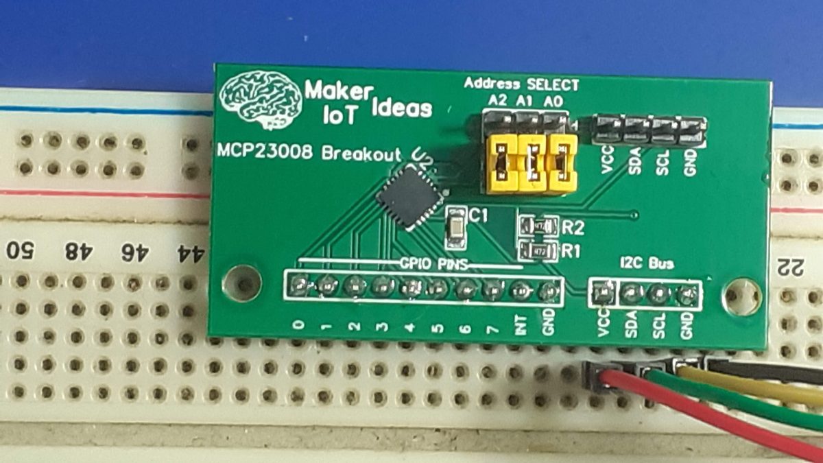
I wanted something as small as possible, and that meant that I chose a QFN package for the MCP23008 IO expander chip. At only 4mm x 4mm, and not being bothered to try and find a DIP version, a breakout board became a much-needed necessity.
Address Selection Jumpers, Two I2C bus headers, and of course the all-important GPIO pins make up all of the user accessible interfacing. Note that the chip reset line is permanently tied to Vcc to make things a bit less cluttered, and easier to use while prototyping.
A decoupling capacitor, as well as pullup resistors on the I2c lines, were also included. Another note here, I did not provide my usual selection jumper to disable these on this particular board.
The Schematic
Manufacturing the PCB
I choose PCBWay for my PCB manufacturing. Why? What makes them different from the rest?
PCBWay‘s business goal is to be the most professional PCB manufacturer for prototyping and low-volume production work in the world. With more than a decade in the business, they are committed to meeting the needs of their customers from different industries in terms of quality, delivery, cost-effectiveness and any other demanding requests. As one of the most experienced PCB manufacturers and SMT Assemblers in China, they pride themselves to be our (the Makers) best business partners, as well as good friends in every aspect of our PCB manufacturing needs. They strive to make our R&D work easy and hassle-free.
How do they do that?
PCBWay is NOT a broker. That means that they do all manufacturing and assembly themselves, cutting out all the middlemen, and saving us money.
PCBWay’s online quoting system gives a very detailed and accurate picture of all costs upfront, including components and assembly costs. This saves a lot of time and hassle.
PCBWay gives you one-on-one customer support, that answers you in 5 minutes ( from the Website chat ), or by email within a few hours ( from your personal account manager). Issues are really resolved very quickly, not that there are many anyway, but, as we are all human, it is nice to know that when a gremlin rears its head, you have someone to talk to that will do his/her best to resolve your issue as soon as possible.
Due to the small size of the QFN package, I strongly recommend that you either have this assembled professionally, or at least consider buying a stencil for applying the solder paste to this board. Maybe those with excellent eyesight can do without that?
Assembly took only a few minutes, with the help of an extremely accurate stencil, followed by a few minutes on a hotplate, and manually soldering on the header pins.
Using the MCP23008 with CircuitPython
I2C devices are very easy to use with the Arduino IDE or similar, and as such, I will not be covering that here.
Circuitpython, however, is gaining popularity, and I am slowly starting to see what the hype is about myself…
So, to get started, you need a microcontroller running CircuitPython – See Adafruit for excellent tutorials. You will also need a few libraries from Adafruit See this link
I will give a very simple example below, showing how to set a pin as an output, as well as an input with internal pullup resistors enabled. Note that the MCP23008 DOES NOT SUPPORT pull-down resistors internally. You need to add those by yourself externally.
# Initialising all the required libraries
import board
import busio
from digitalio import Direction
from adafruit_mcp230xx.mcp23008 import MCP23008
i2c = busio.I2C(board.SCL, board.SDA)
# Adding the MCP23008
mcp = MCP23008(i2c)
# This assumes that you are using the default address [ i.e. all address
# pins are grounded]
#
#
#
# Defining two outputs on pins 0 and 1
pin0 = mcp.get_pin(0)
pin0.direction = Direction.OUTPUT
pin1 = mcp.get_pin(1)
pin1.direction = Direction.OUTPUT
#
#
# We can now control the pins by setting them to true or false, true being
# high
pin0.value = True
pin1.value = True
#
# and switch them off again by using
pin0.value = False
pin1.value = False
#
#
# We can also use the pins as inputs.
# We will activate the internal pullup as well
#
# first , we need another library
import digitalio
pin2 = mcp.get_pin(2)
pin2.direction = digitalio.Direction.INPUT
pin2.pull = digitalio.Pull.UP
#
#
# Reading the pin value is now as easy as
pin2.value
#
# This will return True if the pin is high ( its default state with pullups # activated, of False if pulled low, by for example a switch of button )
Conclusion
The breakout works as expected, and it is very easy to use with CircuitPython. I can now continue with the actual integration and Software for the RP2040 Mouse Rev 2.0 project.
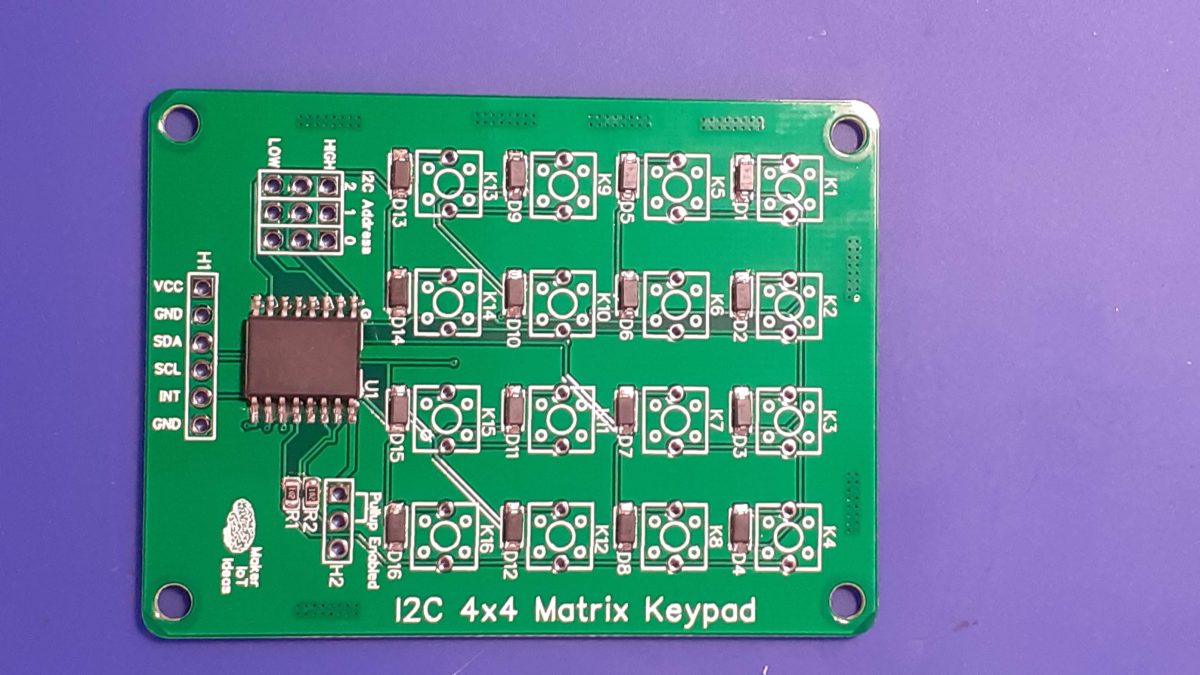
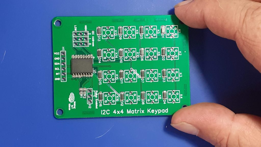
In a previous post this month I introduced my 4×4 matrix keypad. That keypad was designed to be directly interfaced to a microcontroller’s GPIO pins or alternatively to an IO expander chip like the PCF8574. That design, while working very well had the problem of requiring 8 GPIO pins to function correctly.
GPIO pins on a microcontroller can be considered very precious resources, and it should then be logical to assume that we should find a way to use these GPIO pins in a more conservative way, to allow us to interface more peripherals.
I solved this problem by integrating the keypad with an IO Expander on the same PCB. That will allow us to get away with using only 2 GPIO pins, and also open up the option of adding more keypads to the I2C bus, in the event that we need that many keys for a particular project.
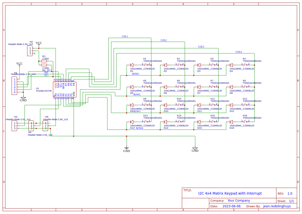
The Schematic
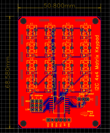
I2C 4×4 Matrix Keypad Schematic
Looking closely at the schematic, we can see that it is exactly the same basic keypad circuit that I used in the initial design. The only difference is that in this design, I have integrated a PCF8574 directly onto the PCB.
Some additional features include selectable I2C Pullup resistors ( usually my microcontroller development boards already include those) that can be activated with a jumper when needed. There are also a set of address selection jumpers, making it possible to stack keypads together into a bigger keyboard if you require something like that. Note that, in this version of the hardware, I did not include headers for stacking.
The keypad can be powered by a DC power source of 3.3v to 5v.
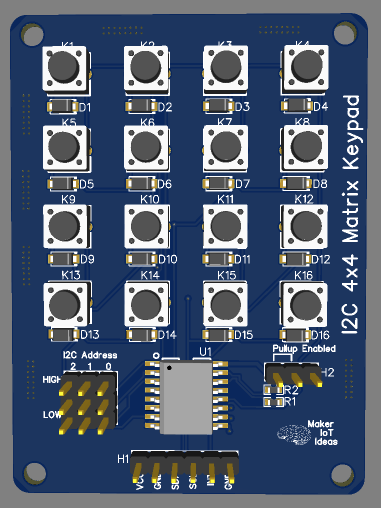
The PCB
I2C Keypad PCB
3D Render of the I2C Keypad
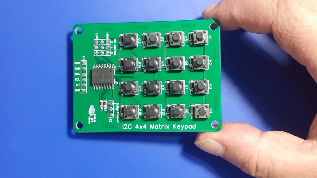
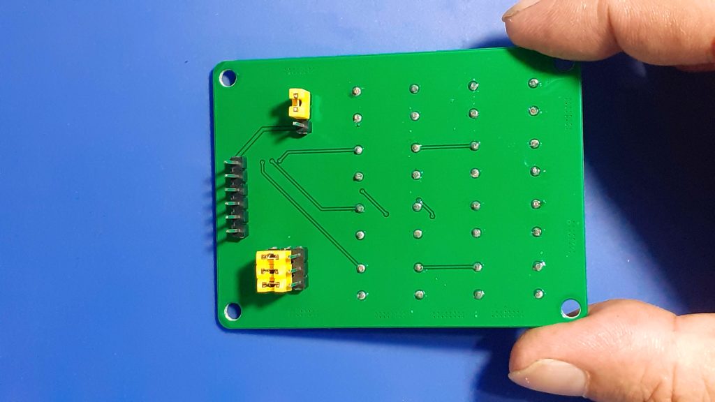
The PCB is a double-layer board of 68.8mm x 50.8mm. Male header pins provide access to the connections as well as address and pullup resistor jumpers. In my build, I have mounted these male headers on the back of the PCB. That makes it possible to mount the Keypad in an enclosure without having the jumpers “stick out” and get in the way.
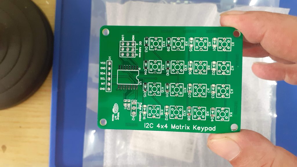
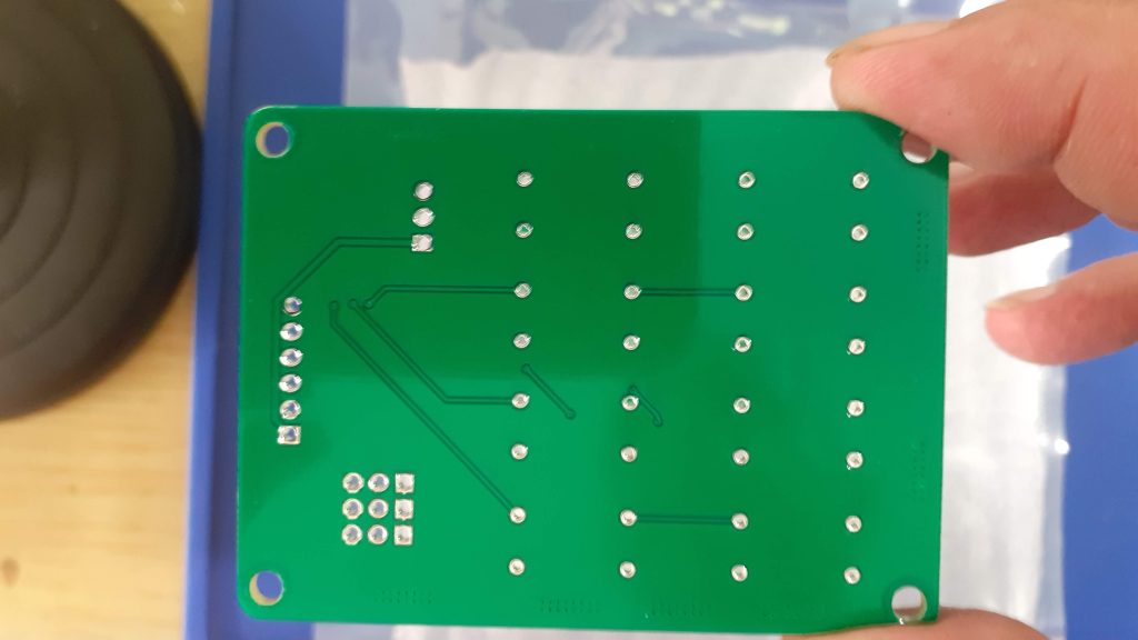
The top layer of the I2C Keypad PCBBottom Layer
Manufacturing
I choose PCBWay for my PCB manufacturing. This month, PCBWay is also celebrating its 9th anniversary, and that means that there are quite a lot of very special offers available.
Why? What makes them different from the rest?
PCBWay‘s business goal is to be the most professional PCB manufacturer for prototyping and low-volume production work in the world. With more than a decade in the business, they are committed to meeting the needs of their customers from different industries in terms of quality, delivery, cost-effectiveness and any other demanding requests. As one of the most experienced PCB manufacturers and SMT Assemblers in China, they pride themselves to be our (the Makers) best business partners, as well as good friends in every aspect of our PCB manufacturing needs. They strive to make our R&D work easy and hassle-free.
How do they do that?
PCBWay is NOT a broker. That means that they do all manufacturing and assembly themselves, cutting out all the middlemen, and saving us money.
PCBWay’s online quoting system gives a very detailed and accurate picture of all costs upfront, including components and assembly costs. This saves a lot of time and hassle.
PCBWay gives you one-on-one customer support, that answers you in 5 minutes ( from the Website chat ), or by email within a few hours ( from your personal account manager). Issues are really resolved very quickly, not that there are many anyway, but, as we are all human, it is nice to know that when a gremlin rears its head, you have someone to talk to that will do his/her best to resolve your issue as soon as possible.
The assembly of this PCB was quite easy and quick. A stencil is not required. All SMD components are 0805 or bigger. It would thus be quite easy to solder them all by hand with a fine-tipped soldering iron.
I have however used soldering paste and hot air to reflow the components, as it is the fastest, in my opinion, and definitely looks neater than hand soldering.
After placing SMD components onto solder paste – ready for reflow solderingAfter Reflow soldering with Hot Air
The board is now ready to solder the switches and header pins in place. As already mentioned above, I chose to assemble the headers on the back of the PCB to prevent them from interfering with any enclosure that I may later use with the keypad.
Final AssemblyNote that I assembled the headers onto the back of the PCB.
Testing and Coding
Testing the keypad consisted of a few steps, the first of which was ensuring that there were no short circuits, as well as that all the momentary switches worked. This was done with a multimeter in continuity as well as diode mode, with probes alternatively on each column and row in turn, while pressing the buttons.
The next stage was testing the I2C IO Expander. This was done with a simple I2C Scanning sketch on an Arduino Uno. It did not do a lot, but, I could see that the PCF8574 is responding to its address and that the pullup resistors work when enabled. This test was repeated with my own ESP8266 and ESP32 boards, this time with pullup resistors disabled, as these boards already have them onboard.
Coding came next, and it was another case of perspectives. It seems like all commercial keypads do not have diodes. This affects the way that they work with a given library. It seems that software developers and hardware developers have different understandings of what a row and a column is.
This meant that, due to the fact that I have diodes on each switch, and the way that the library work – which pins are pulled high and which are set as inputs -, I had to swap around my rows and columns in the software to get everything to work. On a keypad with the diodes replaced with 0-ohm links, that was not needed.
A short test sketch follows below:
Note that with was run on an ESP8266-12E, therefore the Wire.begin() function was changed to Wire.begin(4,5); in order to use GPIO 4 and GPIO 5 for I2C
Another point to note is that the keypad Layout will seem strange. Remember that this is due to the diodes in series on each switch. That forces us to swap around the Rows and the Columns in the software, resulting in a mirrored and rotated left representation of the keypad. It looks funny, but believe me, it actually still works perfectly.
#include <Wire.h>
#include "Keypad.h"
#include <Keypad_I2C.h>

const byte n_rows = 4;
const byte n_cols = 4;

char keys[n_rows][n_cols] = {
    {'1', '4', '7', '*'},
    {'2', '5', '8', '0'},
    {'3', '6', '9', '#'},
    {'A', 'B', 'C', 'D'}};

byte rowPins[n_rows] = {4, 5, 6, 7};
byte colPins[n_cols] = {0, 1, 2, 3};

Keypad_I2C myKeypad = Keypad_I2C(makeKeymap(keys), rowPins, colPins, n_rows, n_cols, 0x20);

String swOnState(KeyState kpadState)
{
    switch (kpadState)
    {
    case IDLE:
        return "IDLE";
        break;
    case PRESSED:
        return "PRESSED";
        break;
    case HOLD:
        return "HOLD";
        break;
    case RELEASED:
        return "RELEASED";
        break;
    } // end switch-case
    return "";
} // end switch on state function

void setup()
{
    // This will be called by App.setup()
    Serial.begin(115200);
    while (!Serial)
    { /*wait*/
    }
    Serial.println("Press any key...");
    Wire.begin(4,5);
    myKeypad.begin(makeKeymap(keys));
}

char myKeyp = NO_KEY;
KeyState myKSp = IDLE;
auto myHold = false;

void loop()
{

    char myKey = myKeypad.getKey();
    KeyState myKS = myKeypad.getState();

    if (myKSp != myKS && myKS != IDLE)
    {
        Serial.print("myKS: ");
        Serial.println(swOnState(myKS));
        myKSp = myKS;
        if (myKey != NULL)
            myKeyp = myKey;
        String r;
        r = myKeyp;
        Serial.println("myKey: " + String(r));
        if (myKS == HOLD)
            myHold = true;
        if (myKS == RELEASED)
        {
            if (myHold)
                r = r + "+";
            Serial.println(r.c_str());
            myHold = false;
        }
        Serial.println(swOnState(myKS));
        myKey == NULL;
        myKS = IDLE;
    }
}
Conclusion
This project once again delivered what I set out to achieve. It has some quirks, but nothing serious. Everything works as expected, both in the Arduino IDE/platform IO realm, as well as in ESPHome. It is worth noting that in ESPHome, we do not need to swap the rows and columns to use the Keypad component. Do remember to leave the has_diodes flag to false though…
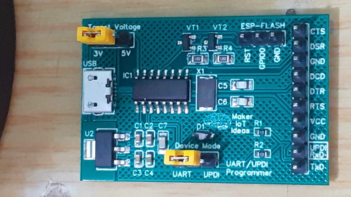
USB-to-Serial converters are some of the most used modules on my bench. I have quite a few of them, most of them are the cheap online type that can be had for a few dollars.
As part of my new project, where I am seriously looking for an alternative chip to replace the ATMEGA328, which has become almost impossible to get, and super expensive when you do get it, I needed to get hold of a UPDI programmer.
There are many available online, from cheap to more expensive, but I wanted to build my own, as it did not seem too difficult to do.
As another part of my daily tasks, I also use a lot of ESP-type chips, which have a particular procedure to upload code via an external serial adapter.
The idea was thus to design a USB UART module that has multiple purposes, as well as being easy and cheap to assemble.
Be able to program ATMEGA328 Chips via Serial
Be able to be used as a standard USB-to-UART adapter
Be a UPDI programmer
Have a selectable target voltage between 3.3v and 5v
Have all modem signals (RTS, CTS, DSR, DTR) broken out.
Be able to auto-flash and reset an ESP32 or ESP8266 device, or similar
The PCB is powered by the PC USB port. The target device voltage is selectable between 3.3v and 5v. The device mode can be changed from UART to UPDI mode with a jumper. An additional header specifically for ESP32/ESP8266 devices is provided, giving access to the FLASH and reset signals for the ESP device.
The USB to serial conversion is taken care of by a CH340G Chip, which provides all the relevant modem signals as well.
All signals, with the exception of the “RING” signal, are broken out onto the main header.
Note that there are NO status or POWER LEDs on the board. This was on purpose, as these sometimes interfere with the UPDI programming mode.
Prototype PCB – Assembled
PCB – TopPCB – Bottom
Connecting to different devices
ESP32 or ESP8266 Devices
When in UART mode, the device can be used to upload code to an ESP32/ESP8266 automatically, similar to a standard dev board, without requiring you to press and flash and reset buttons.
This is achieved by connecting the device as follows:
UART MODULE SET to 3v UART VCC to ESP 3v UART GND to ESP GND UART RX to ESP TX UART TX to ESP RX
(Connections for Auto Upload/Reset) UART RST ( on ESP-Flash Header) to ESP RST UART GPIO0 ( on ESP-Flash Header) to ESP GPIO0
It will now be possible to flash and auto reset the connected ESP device from the Arduino IDE, and possibly others as well…
Arduino (Atmega 328P)
In the current version of the prototype, you have to connect it as follows:
UART Target voltage set to 3v or 5v depending on what type of board you are uploading
UART Tx to Arduino Rx UART Rx to Arduino Tx UART VCC to Arduino 3v or 5v ( depending on the target voltage required by the board you are flashing) UART GND to Arduino GND
To allow for auto flash/reset on the Arduino, a 100nf capacitor is required between the UART DTR line and the Arduino Reset pin. This capacitor has NOT yet been fitted onto the PCB, as I usually use ICSP to upload these. Future versions of the PCB shall have this included.
ATMEGA4808/4809 and or ATTiny with UPDI Interface
This device is currently an LV-only UPDI programmer. Connections are as follows:
Set Target voltage on J1 of the UART/UPDI programmer. Set The Device mode on J2 to UPDI mode
Connect VCC and GND from the Programmer to the target chip/board Connect Programmer UPDI pin( shared with RxD) to Target UPDI pin.
General use UART for use as Serial monitor/Terminal
Set target voltage on J1 Set device mode to UART on J2
Connect VCC, GND from UART to the target device, UART Tx to Target Rx Uart Rx to Target Tx
Optionally connect required modem signals, RTS, CTS, DTR, and DSR as needed
Manufacturing
The PCB for this project has been manufactured at PCBWay. Please consider supporting them if you would like your own copy of this PCB, or if you have any PCB of your own that you need to have manufactured.
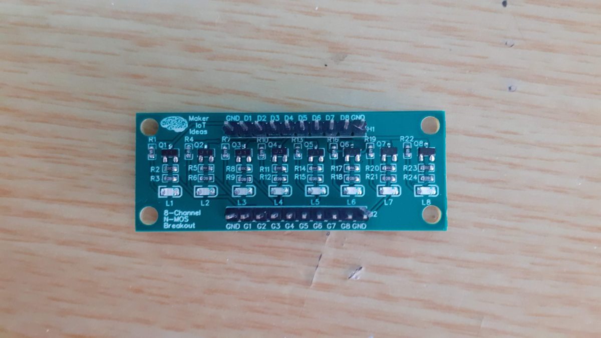
As a companion module to my recently published 8Ch PMOD breakout board, I decided to do a similar PCB, but with NMOS devices instead. This opens up more possibilities for proper testing and prototyping, as PMOS and NMOS devices has different use applications, and most importantly, can sometimes even be combined for a particular purpose, like an H-Bridge motor driver, for example.
8Ch NMOS Breakout
What is on the PCB?
As NMOS devices function quite differently from their PMOS counterparts, it did not make sense to reuse the PMOS board, and just change the devices… although some people may be tempted to think you could…
The N Channel Mosfet basically “works in mirrored mode” from a P Channel one, and is used to do so-called ” LOW Side switching” which means that your load connects to the positive power rail, and then to the DRAIN pin of the MOSFET, with the source being connected to ground… ( It can sometimes also be used the other way around… but lets not go there now….
The current prototype PCB contains 8 BSS138 NMOS Mosfets, in my case, with is capable of about 800mA of current… All source pins are internally connected to ground. This forces you to use this module as a low side switch…
Two 10-way 2.54mm headers are provided, with a ground pin on Pin 1 and 10 of each of these.
The Drain pins of each NMOS device is available on the top header, labeled D1 through D8, and the Gate pins of each respective NMOS device is available on the bottom header, labelled G1 through G8.
Each gate has a pull-down resistor to ground, to keep it from flapping around, as well as a gate resistor. In my case, I selected to use a 10k pulldown, and a 1k gate resistor, as that is sufficient for my general needs…
Each NMOS device also has a LED signal indicator, to assist in visual confirmation of a specific channel’s state.
PCB Top Side
The Schematic
Schematic
Using the breakout
The module is very easy to use, and as briefly mentioned above, you are only required to connect one side of your load to the positive supply rail, and the other side to the drain pin of your choice.
Connect the ground pins of the module to your ground rail.
The Gate pin, with a corresponding number to the drain you have selected, can now be connected to your GPIO of choice on a microcontroller.
Drive the pin High to switch on the load, drive it log to switch off. Easy.
Please note: While the NMOS devices used on the board can handle quite a lot of current, (800mA in the case of the BSS138), it is not recommended to try and pull too much current through a single channel. The PCB traces can safely handle about a maximum of 300 to 400mA per channel.
PCB Bottom
Manufacturing
The PCB for this project has been manufactured at PCBWay. Please consider supporting them if you would like your own copy of this PCB, or if you have any PCB of your own that you need to have manufactured.
Example code for using the breakout (Arduino)
// Example code for 8Ch NMOS breakout
int Gate1 9;
int Gate2 10;

void setup() {
  // drive the two gate pins low to ensure NMOS devices
  // are in a positively known state at startup
  digitalWrite(Gate1,LOW);
  digitalWrite(Gate2,LOW);
  // Set gpio to output mode
  pinMode(Gate1,OUTPUT);
  pinMode(Gate2,OUTPUT);

}

void loop() {
  // Toggle the two channels in an alternating pattern
  digitalWrite(Gate1,!digitalRead(Gate1));
  digitalWrite(Gate2,!digitalRead(Gate1));
  delay(1000);

}
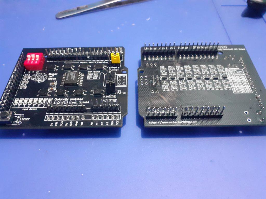
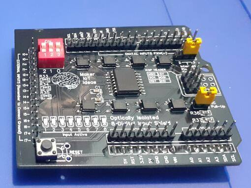
Welcome to the final instalment of my 8 DI Optically Isolated Arduino Shield. Today I will show you some of the assembly pictures, as well as look at the coding to use this shield. I will also provide you with a link to the manufacturing files, in case you want to make your own.
You can order your own version of this board for just $5 USD if you click here
PCBWay makes it quite easy to order prototypes for your PCB’s… Just upload the Gerber files on their website, select your desired options for the PCB and order. The turn-around time is great. I received these boards, ordered together with a stencil for SMD assembly, in exactly 5 days, shipping from China to Thailand 🙂 That is super fast, as it arrived 4 days faster than the components that were ordered locally from Bangkok! Be sure to consider using their services next time you need a PBC made…
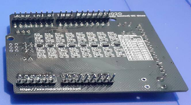
Top and bottom layout of completed Shield
Bottom of Shield
Top Layout
Some notes on assembly: The reset switch will seem misplaced, and indeed, it is 🙂 The reason for this is that I could not get any 4 pin tactile switches 🙁 So I had to either leave it unpopulated or use a two-pin tactile switch. As I will be using these shields myself, I decided that although it doesn’t look perfect, the two pin switch will still provide me with the functionality that I want.
On the bottom of the board, you can still see some blobs of flux, as the pictures were taken right after assembly, and have not been cleaned up yet. Some solder joints have also not been cleaned up yet.
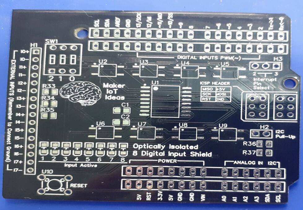
The top of the unpopulated PCBThe bottom of the PCB
Testing and Coding
The testing of the board is quite straightforward. I first checked all the power rails with a multimeter to make sure there are no open circuits of shorts. Then I checked connections to all the chips and other components, yes, it takes a while to do that, but rather safe than sorry. After assembly, I repeated this process, making sure that all the components receive the correct power level, and that all switches ( like for addressing and the reset button ) actually do what I intended them to do. The next tests were the individual inputs with the optocouplers. This is done by connecting an input source (between 5.5v and 32v) to each individual input and then physically testing on the pins of the optocoupler in question, for the correct voltage input.
The shield is then powered from 5v and the input test is repeated while checking with a multimeter that the input signal does indeed get transferred by the optocoupler to the PCF8574 chip. I found that with the particular batch of PCF8574 chips that I got, that the IC would only respond reliably with a voltage between 5.5v and 32v. The original design was for 3.0v to 32v. I found that the Optocoupler EL357N seems to be unable to switch itself on at the low current allowed through the resistor divider at the input. This can be fixed by lowering the value of R1, R5, R9, R13, R17, R21, R25, R27 from 4k7 to whatever value you need. Note that that will reduce the top-level input voltage that you can safely use. For my application, however, 5.5v to 24v will be perfect, so I will leave it as is.
The shield is now connected to an Arduino with DuPont Wires, to test the I2C addressing of the PCF8574. The chip address is changed with the 3-way dip switch at SW1. All eight addresses are available. It should be noted that I have used a pull-up configuration on the address lines. That will reverse your logic.. Switching the dip switch on will pull the pin to GND, not to VCC as you would normally expect. Thus as an example, all switches off will give an address 0f 0x3f, while all on will give 0x38.
Coding
You can use the standard Arduino IDE with the Wire.h library to code the shield, or you can use one of the many PCF8574 libraries that are available. I coded my tests with the Embeetle IDE, as it gives me much better control over my code. I will show you a short, interrupt enabled sketch, in Arduino C++ below
#include <Wire.h>

byte _portStatus = 0b00000000;
boolean _readI2C = false;

void MyISR() { // Interrupt service routine
  //Serial.println("Interrupt Occured on Pin2");
  if (_readI2C != true) {
    _readI2C = true;
  }
}

void setup() {
  // put your setup code here, to run once:
  pinMode(2,INPUT_PULLUP);
  attachInterrupt(digitalPinToInterrupt(2),MyISR,FALLING);
  Serial.begin(115200);
  Wire.begin();
  Wire.beginTransmission(0x20);
  Wire.write(0xFF); // set all pins to 1, needed to make them inputs
  Wire.endTransmission();
}

void loop() {
  // put your main code here, to run repeatedly:

  byte _data;
  if (_readI2C == true) {
    _readI2C = false;
    Wire.requestFrom(0x20,1);
    if (Wire.available()) {
      _data = Wire.read();
    }
  }
  if (_portStatus != _data) {
    Serial.print("Port Data Changed : 0xb");
    Serial.print(_portStatus,BIN);
    Serial.print(" changed to : 0xb");
    Serial.println(_data,BIN);
    _portStatus = _data;
    delay(50);
  } else {
    _portStatus = _portStatus;
  }

}
Conclusion
This turned out to be a very interesting and fun project to do. From designing the circuit to getting it manufactured and hand assembling it myself was a very satisfying experience. I would like to take this opportunity to thank Wendy Wu, from PCBWay‘s Marketing department, for her assistance with the manufacturing of the board. The speed and efficiency with which she handled this project were fantastic.
Today I will show you another useful IO Expander chip, The MCP23017. This chip, although similar to the PCF8475, which I have already covered in a previous article, has many additional features that may make it a very attractive solution when you need some more extra GPIO pins for a big project…
Features
Let us look at some of the features of this chip
16-Bit Remote Bidirectional I/O Port:
I/O pins default to input • High-Speed I2C Interface (MCP23017):
100 kHz
400 kHz
1.7 MHz • High-Speed SPI Interface (MCP23S17):
10 MHz (maximum) • Three Hardware Address Pins to Allow Up to Eight Devices On the Bus • Configurable Interrupt Output Pins:
Configurable as active-high, active-low or open-drain • INTA and INTB Can Be Configured to Operate Independently or Together • Configurable Interrupt Source:
Interrupt-on-change from configured register defaults or pin changes • Polarity Inversion Register to Configure the Polarity of the Input Port Data • External Reset Input • Low Standby Current: 1 µA (max.) • Operating Voltage:
1.8V to 5.5V @ -40°C to +85°C
2.7V to 5.5V @ -40°C to +85°C
4.5V to 5.5V @ -40°C to +125°C
MCP23017 Pinout Diagram
The sixteen I/O ports are separated into two ‘ports’ – A (on the right) and B (on the left. Pin 9 connects to 5V, 10 to GND, 11 isn’t used, 12 is the I2C bus clock line (Arduino Uno/Duemilanove analogue pin 5, Mega pin 21), and 13 is the I2C bus data line (Arduino Uno/Duemailnove analogue pin 4, Mega pin 20).
External pull-up resistors should be used on the I2C bus – in our examples we use 4.7k ohm values. Pin 14 is unused, and we won’t be looking at interrupts, so ignore pins 19 and 20. Pin 18 is the reset pin, which is normally high – therefore you ground it to reset the IC. So connect it to 5V!
Finally we have the three hardware address pins 15~17. These are used to determine the I2C bus address for the chip. If you connect them all to GND, the address is 0x20. If you have other devices with that address or need to use multiple MCP23017s, see figure 1-2 in the datasheet.
You can alter the address by connecting a combination of pins 15~17 to 5V (1) or GND (0). For example, if you connect 15~17 all to 5V, the control byte becomes 0100111 in binary, or 0x27 in hexadecimal.
It is also available on a convenient breakout PCB, for about $USD0.80 from AliExpress
MCP23017 on Breakout PCB – Back
MCP23017 on Breakout PCB – Front
Please Note: THIS BREAKOUT PCB IS NOT SUITED FOR USE ON A BREADBOARD. YOU WILL SHORT OUT VCC AND GROUND AS WELL AS ALL THE IO PINS IF YOU TRY TO USE IT ON A BREADBOARD.
As you can see, the pins are however very clearly labelled, and thus easy to use. I have also purposely soldered my header pins “the wrong way round” to prevent using it on a breadboard, as this will short out Vcc to Ground!
Having interrupt outputs is one of the most important features of the MCP23017, since the microcontroller does not have to continuously poll the device to detect an input change. Instead an interrupt service routine can be used to react quickly to an input change such a key press…
To make life even easier each GPIO input pin can be configured with an internal pullup (~100k) and that means you won’t have to wire up external pull up resistors for keyboard input. You can also mix and match inputs and outputs the same as any standard microcontroller 8 bit port.
Addressing
The 23017 has three input pins to allow you to set a different address for each attached MCP23017.
The above corresponds to a hardware address for the three lines A0, A1, A2 corresponding to the input pin values at the IC. You must set the value of these hardware inputs as 0V or (high) volts and not leave them floating otherwise they will get random values from electrical noise and the chip will do nothing!
The four left most bits are fixed a 0100 (specified by a consortium who doles out address ranges to manufacturers).
So the MCP23017 I2C address range is 32 decimal to 37 decimal or 0x20 to 0x27 for the MCP23017.
Please note: The addresses are the same as those for the PCF8475. You must thus be careful if you use these two devices on the same i2c bus!
MCP23017 Non interrupt registers
IODIR I/O direction register
For controlling I/O direction of each pin, register IODIR (A/B) lets you set the pin to an output when a zero is written and to an input when a ‘1’ is written to the register bit. This is the same scheme for most microcontrollers – the key is to remember that zero (‘0’) equates to the ‘O’ in Output.
GPPU Pullup register
Setting a bit high sets the pullup active for the corresponding I/O pin.
OLAT Output Latch register
This is exactly the same as the I/O port in 18F series PIC chips where you can read back the “desired” output of a port pin whether or not the actual state of that pin is reached. i.e. consider a strong current LED attached to the pin – it is easily possible to pull down the output voltage at the pin to below the logic threshold i.e. you would read back a zero if reading from the pin itself when in fact it should be a one. Reading the OLAT register bit returns a ‘one’ as you would expect from a software engineering point of view.
IPOL pin inversion register
The IPOL(A/B) register allows you to selectively invert any input pin. This reduces the glue logic needed to interface other devices to the MCP23017 since you won’t need to add inverter logic chips to get the correct signal polarity into the MCP23017.
It is also very handy for getting the signals the right way up e.g. it is common to use a pull up resistor for an input so when a user presses an input key the voltage input is zero, so in software you have to remember to test for zero.
Using the MCP23017 you could invert that input and test for a 1 (in my mind a key press is more equivalent to an on state i.e. a ‘1’) however I use pullups all the time (and uCs in general use internal pullups when enabled) so have to put up with a zero as ‘pressed’. Using this device would allow you to correct this easily.Note: The reason that active low signals are used everywhere is a historical one: TTL (Transistor Transistor Logic) devices draw more power in the active low state due to the internal circuitry, and it was important to reduce unnecessary power consumption – therefore signals that are inactive most of the time e.g. a chip select signal – were defined to be high. With CMOS devices either state causes the same power usage so it now does not matter – however active low is used because everyone uses it now and used it in the past.
SEQOP polling mode : register bit : (Within IOCON register)
If you have a design that has critical interrupt code e.g. for performing a timing critical measurement you may not want non critical inputs to generate an interrupt i.e. you reserve the interrupt for the most important input data.
In this case, it may make more sense to allow polling of some of the device inputs. To facilitate this “Byte mode” is provided. In this mode, you can read the same set of GPIOs using clocks but not needling to provide other control information. i.e. it stays on the same set of GPIO bits, and you can continuously read it without the register-address updating itself. In non-byte mode, you either have to set the address you read from (A or B bank) as control input data.
Now to examine how to use the IC in our sketches.
As you should know by now most I2C devices have several registers that can be addressed. Each address holds one byte of data that determines various options. So before using we need to set whether each port is an input or an output. First, we’ll examine setting them as outputs. So to set port A to outputs, we use:
Wire.beginTransmission(0x20);
Wire.write(0x00); // IODIRA register
Wire.write(0x00); // set all of port A to outputs
Wire.endTransmission();
Then to set port B to outputs, we use:
Wire.beginTransmission(0x20);
Wire.write(0x01); // IODIRB register
Wire.write(0x00); // set all of port B to outputs
Wire.endTransmission();
So now we are in void loop() or a function of your own creation and want to control some output pins. To control port A, we use:
Wire.beginTransmission(0x20);
Wire.write(0x12); // address port A
Wire.write(??);  // value to send
Wire.endTransmission();
To control port B, we use:
Wire.beginTransmission(0x20);
Wire.write(0x13); // address port B
Wire.write(??);  // value to send
Wire.endTransmission();
… replacing ?? with the binary or equivalent hexadecimal or decimal value to send to the register.
To calculate the required number, consider each I/O pin from 7 to 0 matches one bit of a binary number – 1 for on, 0 for off. So you can insert a binary number representing the status of each output pin. Or if binary does your head in, convert it to hexadecimal. Or a decimal number.
So for example, you want pins 7 and 1 on. In binary that would be 10000010, in hexadecimal that is 0x82, or 130 decimal. (Using decimals is convenient if you want to display values from an incrementing value or function result).
For example, we want port A to be 11001100 and port B to be 10001000 – so we send the following (note we converted the binary values to decimal):
Wire.beginTransmission(0x20);
Wire.write(0x12); // address port A
Wire.write(204); // value to send
Wire.endTransmission();
Wire.beginTransmission(0x20);
Wire.write(0x13); // address port B
Wire.write(136);     // value to send
Wire.endTransmission();
A complete Example
// pins 15~17 to GND, I2C bus address is 0x20
#include "Wire.h"
void setup()
{
 Wire.begin(); // wake up I2C bus
// set I/O pins to outputs
 Wire.beginTransmission(0x20);
 Wire.write(0x00); // IODIRA register
 Wire.write(0x00); // set all of port A to outputs
 Wire.endTransmission();
Wire.beginTransmission(0x20);
 Wire.write(0x01); // IODIRB register
 Wire.write(0x00); // set all of port B to outputs
 Wire.endTransmission();
}
void binaryCount()
{
 for (byte a=0; a<256; a++)
 {
 Wire.beginTransmission(0x20);
 Wire.write(0x12); // GPIOA
 Wire.write(a); // port A
 Wire.endTransmission();
Wire.beginTransmission(0x20);
 Wire.write(0x13); // GPIOB
 Wire.write(a); // port B
 Wire.endTransmission();
 }
}
void loop()
{
 binaryCount();
 delay(500);
}
Using the pins as inputs
Although that may have seemed like a simple demonstration, it was created show how the outputs can be used. So now you know how to control the I/O pins set as outputs. Note that you can’t source more than 25 mA of current from each pin, so if switching higher current loads use a transistor and an external power supply and so on.
Now let’s turn the tables and work on using the I/O pins as digital inputs. The MCP23017 I/O pins default to input mode, so we just need to initiate the I2C bus. Then in the void loop() or other function all we do is set the address of the register to read and receive one byte of data.
// pins 15~17 to GND, I2C bus address is 0x20
#include "Wire.h"
byte inputs=0;
void setup()
{
 Serial.begin(9600);
 Wire.begin(); // wake up I2C bus
}
void loop()
{
 Wire.beginTransmission(0x20);
 Wire.write(0x13); // set MCP23017 memory pointer to GPIOB address
 Wire.endTransmission();
 Wire.requestFrom(0x20, 1); // request one byte of data from MCP20317
 inputs=Wire.read(); // store the incoming byte into "inputs"
 if (inputs>0) // if a button was pressed
 {
 Serial.println(inputs, BIN); // display the contents of the GPIOB register in binary
 delay(200); // for debounce
 }
}
Other Libraries
You can also download and install the MCP23017 Library from Adafruit for the Arduino IDE. This library will make using this chip even easier… I will discuss this library in another post
The Serial Peripheral Interface is a synchronous serial communication interface for short-distance communication, it is typically used in embedded systems. The interface was developed by Motorola in the mid 1980’s and has become a very popular standard.
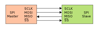
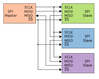
It is used with many kinds of sensors, LCD’s and also SD-Cards. SPI operates in a Master-Slave model, with a possibility of multiple slave devices, each selected in turn by a SS (slave select) or CS (chip select) pin that is usually pulled low by the master.
Typical connection between two SPI devices
Typical configuration
SPI is a four-wire interface, with the different lines being – MOSI [Master Out Slave In] -MISO [Master In Slave Out] -SCLK [Serial Clock OUT – generated by the master] -SS/CS [Slave Select or Chip Select, sometimes also labelled CE – Chip Enable]
SPI is a FULL DUPLEX interface, where the master initiates the communication frames between the various slave devices. This is usually done by pulling the particular device’s SS/CS pin low. Data is then shifted simultaneously into and out of the devices by means of the MOSI and MISO lines on the bus. The frequency of the serially shifted data is controlled by the SCLK line. This clock signal is generated by the master device.
It is important to note that MOST of the slave devices have a tri-state (HIGH IMPEDANCE) mode on their MISO pins. This electrically disconnects the MISO pin from the bus when the device is not selected via the SS/CS pin.
You should also note the SPI slave devices that do not have a tri-state mode on their MISO pins, should not be used on the same bus as devices that have without using an external tri-state buffer circuit between the non-tristate device and the rest of the devices on the MISO bus.
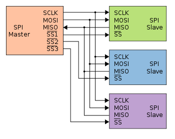
Typical connection between an SPI Master and three Slave devices
It is possible to connect multiple SPI slave devices to on Master device if you remember that each slave device will need its own dedicated SS/CS pin on the master. This can however quickly use a lot of IO pins on a microcontroller, thus being one of the disadvantages of SPI versus I2C. SPI is however quite a bit faster than I2C.
Data Transmission
To begin communication, the bus master configures the clock, using a frequency supported by the slave device, typically up to a few MHz. The master then selects the slave device with a logic level 0 on the select line. If a waiting period is required, such as for an analog-to-digital conversion, the master must wait for at least that period of time before issuing clock cycles.
During each SPI clock cycle, full-duplex data transmission occurs. The master sends a bit on the MOSI line and the slave reads it, while the slave sends a bit on the MISO line and the master reads it. This sequence is maintained even when only one-directional data transfer is intended.
A typical hardware setup using two shift registers to form an inter-chip circular buffer
Transmissions normally involve two shift registers of some given word-size, such as eight bits, one in the master and one in the slave; they are connected in a virtual ring topology. Data is usually shifted out with the most significant bit first. On the clock edge, both master and slave shift out a bit and output it on the transmission line to the counterpart. On the next clock edge, at each receiver the bit is sampled from the transmission line and set as a new least-significant bit of the shift register. After the register bits have been shifted out and in, the master and slave have exchanged register values. If more data needs to be exchanged, the shift registers are reloaded and the process repeats. Transmission may continue for any number of clock cycles. When complete, the master stops toggling the clock signal, and typically deselects the slave.
Transmissions often consist of eight-bit words. However, other word-sizes are also common, for example, sixteen-bit words for touch-screen controllers or audio codecs, such as the TSC2101 by Texas Instruments, or twelve-bit words for many digital-to-analogue or analogue-to-digital converters.
Every slave on the bus that has not been activated using its chip select line must disregard the input clock and MOSI signals and should not drive MISO (I.E. must have a tri-state output) although some devices need external tri-state buffers to implement this.
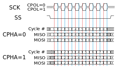
Clock polarity and phasing
In addition to setting the clock frequency, the master must also configure the clock polarity and phase with respect to the data. Motorola SPI Block Guide names these two options as CPOL and CPHA (for clock polarity and phase) respectively, a convention most vendors have also adopted.
The timing diagram is shown below. The timing is further described below and applies to both the master and the slave device.
CPOL determines the polarity of the clock. The polarities can be converted with a simple inverter.
CPOL=0 is a clock which idles at 0, and each cycle consists of a pulse of 1. That is, the leading edge is a rising edge, and the trailing edge is a falling edge.
CPOL=1 is a clock which idles at 1, and each cycle consists of a pulse of 0. That is, the leading edge is a falling edge, and the trailing edge is a rising edge.
CPHA determines the timing (i.e. phase) of the data bits relative to the clock pulses. Conversion between these two forms is non-trivial.
For CPHA=0, the “out” side changes the data on the trailing edge of the preceding clock cycle, while the “in” side captures the data on (or shortly after) the leading edge of the clock cycle. The out-side holds the data valid until the trailing edge of the current clock cycle. For the first cycle, the first bit must be on the MOSI line before the leading clock edge.
An alternative way of considering it is to say that a CPHA=0 cycle consists of a half cycle with the clock idle, followed by a half cycle with the clock asserted.
For CPHA=1, the “out” side changes the data on the leading edge of the current clock cycle, while the “in” side captures the data on (or shortly after) the trailing edge of the clock cycle. The out-side holds the data valid until the leading edge of the following clock cycle. For the last cycle, the slave holds the MISO line valid until slave select is de-selected.
An alternative way of considering it is to say that a CPHA=1 cycle consists of a half cycle with the clock asserted, followed by a half cycle with the clock idle.
A timing diagram showing clock polarity and phase. Red lines denote clock leading edges, and blue lines, trailing edges.
The MOSI and MISO signals are usually stable (at their reception points) for the half cycle until the next clock transition. SPI master and slave devices may well sample data at different points in that half cycle.
This adds more flexibility to the communication channel between the master and slave.
Mode numbers
The combinations of polarity and phases are often referred to as modes which are commonly numbered according to the following convention, with CPOL as the high order bit and CPHA as the low order bit:
For “Microchip PIC” / “ARM-based” microcontrollers (note that NCPHA is the inversion of CPHA):
SPI mode
Clock polarity (CPOL/CKP)
Clock phase (CPHA)
Clock edge (CKE/NCPHA)
0
0
0
1
1
0
1
0
2
1
0
1
3
1
1
0
For PIC32MX: SPI mode configure CKP, CKE and SMP bits. Set SMP bit and CKP, CKE two bits configured as above table.
Mode
CPOL
CPHA
0
0
0
1
0
1
2
1
0
3
1
1
For other microcontrollers:
Another commonly used notation represents the mode as a (CPOL, CPHA) tuple; e.g., the value ‘(0, 1)’ would indicate CPOL=0 and CPHA=1.
Note that in Full Duplex operation, the Master device could transmit and receive with different modes. For instance, it could transmit in Mode 0 and be receiving in Mode 1 at the same time.
Independent Slave Configuration
In the independent slave configuration, there is an independent chip select line for each slave. This is the way SPI is normally used. The master asserts only one chip select at a time.
Pull-up resistors between the power source and chip select lines are recommended for systems where the master’s chip select pins may default to an undefined state. When separate software routines initialize each chip select and communicate with its slave, pull-up resistors prevent other uninitialized slaves from responding.
Since the MISO pins of the slaves are connected together, they are required to be tri-state pins (high, low or high-impedance), where the high-impedance output must be applied when the slave is not selected. Slave devices not supporting tri-state may be used in independent slave configuration by adding a tri-state buffer chip controlled by the chip select signal. (Since only a single signal line needs to be tri-stated per slave, one typical standard logic chip that contains four tristate buffers with independent gate inputs can be used to interface up to four slave devices to an SPI bus.)
Typical SPI configuration
Daisy chain configuration
Some products that implement SPI may be connected in a daisy chain configuration, the first slave output being connected to the second slave input, etc. The SPI port of each slave is designed to send out during the second group of clock pulses an exact copy of the data it received during the first group of clock pulses. The whole chain acts as a communication shift register; daisy chaining is often done with shift registers to provide a bank of inputs or outputs through SPI. Each slave copies input to output in the next clock cycle until the active low SS line goes high. Such a feature only requires a single SS line from the master, rather than a separate SS line for each slave.
Note that not all SPI devices support this. You should thus check your datasheet before using this configuration!
SPI Daisy Chain configuration
Valid Communications
Some slave devices are designed to ignore any SPI communications in which the number of clock pulses is greater than specified. Others do not care, ignoring extra inputs and continuing to shift the same output bit. It is common for different devices to use SPI communications with different lengths, as, for example, when SPI is used to access the scan chain of a digital IC by issuing a command word of one size (perhaps 32 bits) and then getting a response of a different size (perhaps 153 bits, one for each pin in that scan chain).
Interrupts
SPI devices sometimes use another signal line to send an interrupt signal to a host CPU. Examples include pen-down interrupts from touchscreen sensors, thermal limit alerts from temperature sensors, alarms issued by real-time clock chips, SDIO, and headset jack insertions from the sound codec in a cell phone. Interrupts are not covered by the SPI standard; their usage is neither forbidden nor specified by the standard. In other words, interrupts are outside the scope of the SPI standard and are optionally implemented independently from it.
Bit Banging a SPI Master – Example code
Below is an example of bit-banging the SPI protocol as an SPI master with CPOL=0, CPHA=0, and eight bits per transfer. The example is written in the C programming language. Because this is CPOL=0 the clock must be pulled low before the chip select is activated. The chip select line must be activated, which normally means being toggled low, for the peripheral before the start of the transfer, and then deactivated afterwards. Most peripherals allow or require several transfers while the select line is low; this routine might be called several times before deselecting the chip.
/*
 * Simultaneously transmit and receive a byte on the SPI.
 *
 * Polarity and phase are assumed to be both 0, i.e.:
 *   - input data is captured on rising edge of SCLK.
 *   - output data is propagated on falling edge of SCLK.
 *
 * Returns the received byte.
 */
uint8_t SPI_transfer_byte(uint8_t byte_out)
{
    uint8_t byte_in = 0;
    uint8_t bit;

    for (bit = 0x80; bit; bit >>= 1) {
        /* Shift-out a bit to the MOSI line */
        write_MOSI((byte_out & bit) ? HIGH : LOW);

        /* Delay for at least the peer's setup time */
        delay(SPI_SCLK_LOW_TIME);

        /* Pull the clock line high */
        write_SCLK(HIGH);

        /* Shift-in a bit from the MISO line */
        if (read_MISO() == HIGH)
            byte_in |= bit;

        /* Delay for at least the peer's hold time */
        delay(SPI_SCLK_HIGH_TIME);

        /* Pull the clock line low */
        write_SCLK(LOW);
    }

    return byte_in;
}
This concludes part 1 of my series on SPI. I hope you found it interesting and useful.
Adding a display to any project can instantly increase its visual appeal, as well as make the project easier to control. Displays available to Electronic enthusiasts mostly include some sort of LCD or even TFT display. LCD displays are usually bulky and very limited in their ability to display a lot of information, whereas TFT type displays are still a bit on the expensive side, and not very easy to interface with for the beginner.
Today, I would like to introduce a different type of display, which is available in an I2C as well as SPI version. These displays are very easily readable in almost any light conditions, lightweight, and most importantly, they are extremely cheap. I am talking about the OLED display of course… Many of us may already have one of them in our mobile phones, or even TV screen…
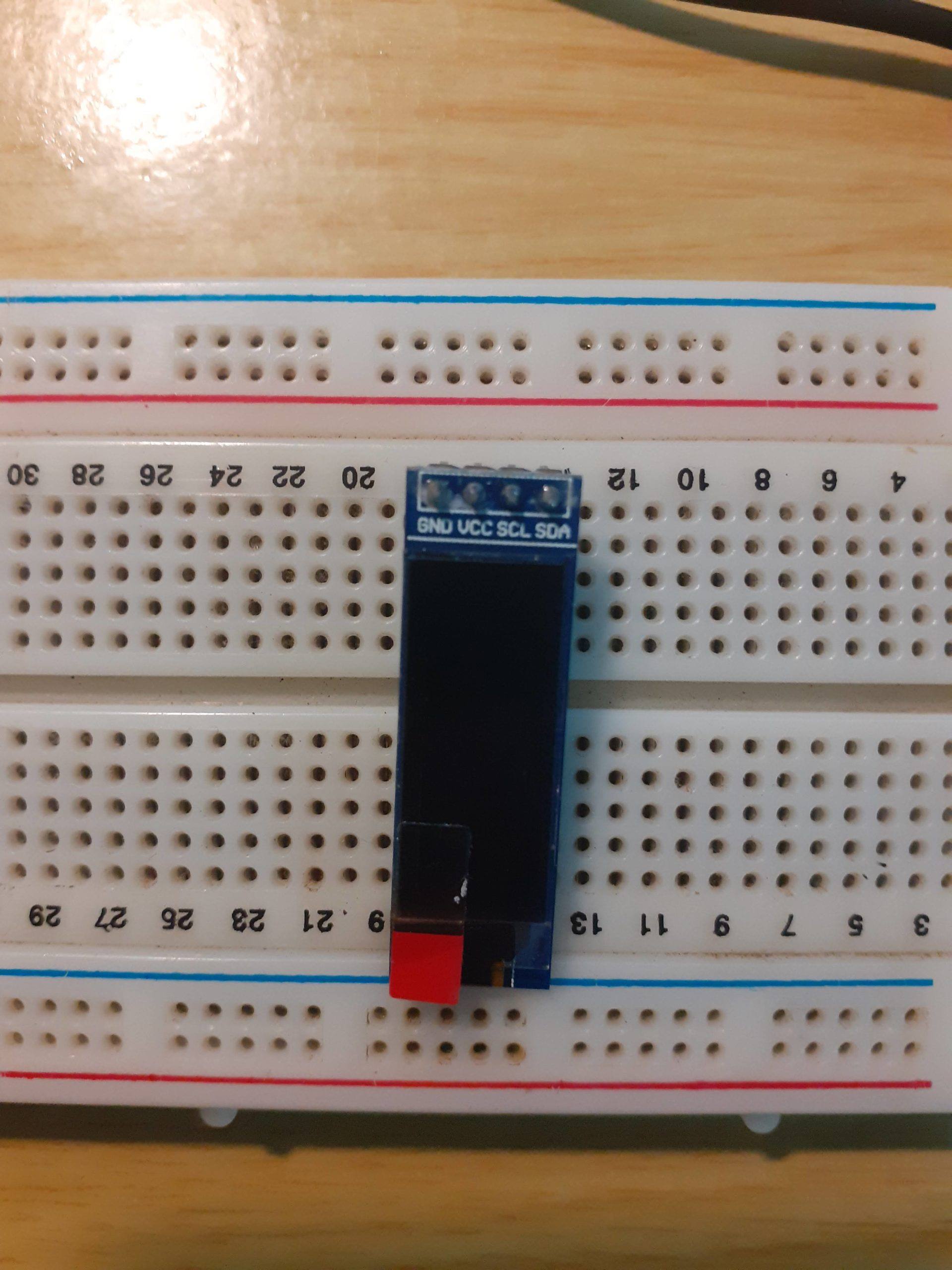
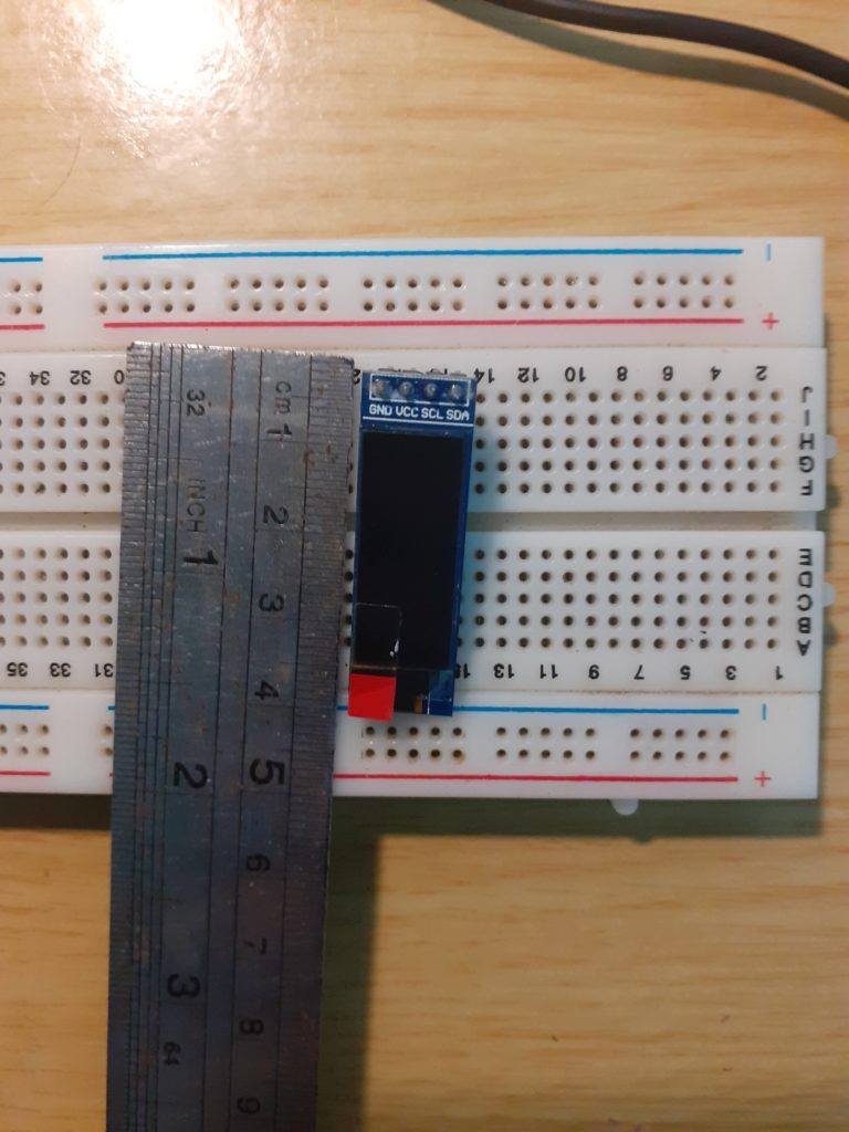
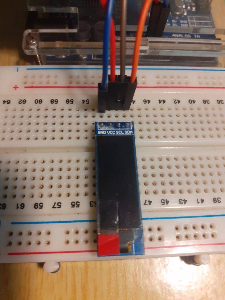
128×32 I2C OLED Display (40mmx10mm) [0.91″] Front view
There are two main families of OLED: those based on small molecules and those employing polymers. Adding mobile ions to an OLED creates a light-emitting electrochemical cell (LEC) which has a slightly different mode of operation. An OLED display can be driven with a passive-matrix (PMOLED) or active-matrix (AMOLED) control scheme. In the PMOLED scheme, each row (and line) in the display is controlled sequentially, one by one,[6] whereas AMOLED control uses a thin-film transistor backplane to directly access and switch each individual pixel on or off, allowing for higher resolution and larger display sizes.
An OLED display works without a backlight because it emits visible light. Thus, it can display deep black levels and can be thinner and lighter than a liquid crystal display (LCD). In low ambient light conditions (such as a dark room), an OLED screen can achieve a higher contrast ratio than an LCD, regardless of whether the LCD uses cold cathode fluorescent lamps or an LED backlight. OLED displays are made in the same way as LCDs, but after TFT (for active matrix displays), addressable grid (for passive matrix displays) or ITO segment (for segment displays) formation, the display is coated with hole injection, transport and blocking layers, as well with electroluminescent material after the 2 first layers, after which ITO or metal may be applied again as a cathode and later the entire stack of materials is encapsulated. The TFT layer, addressable grid or ITO segments serve as or are connected to the anode, which may be made of ITO or metal.[7][8] OLEDs can be made flexible and transparent, with transparent displays being used in smartphones with optical fingerprint scanners and flexible displays being used in foldable smartphones.
The full article is available here if you are interested.
128×32 I2C OLED Display (40mmx10mm) [0.91″] Back view
Connecting the circuit
This display is once again extremely easy to connect, as it uses the very versatile I2C protocol. (An SPI version is also available).
Connecting 128×32 OLED display to an Arduino Uno Clone
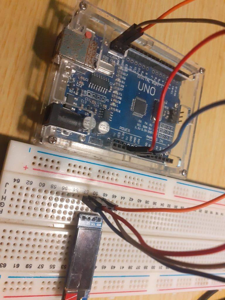
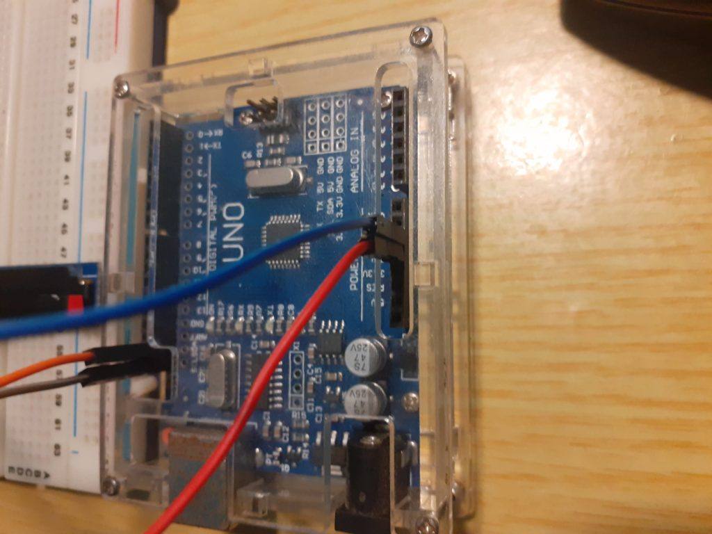
A Closeup view of the wiring. Red = +5v, Blue = GND (0v), Orange = SDA, Brown = SCL
Connect the following wires to the Arduino / ESP32 +5v (red) to the VCC pin on the display Gnd to Gnd SDA (A4 on Uno) to SDA, and SCL (A5 on Uno) to SCL
The Software Libraries
The 128×32 OLED display that we will be using today, is based on the SSD1306. We will thus be using a library suplied by Adafruit to interface with this chip. There are various other libraries available, but I have found the Adafruit library the most stable.
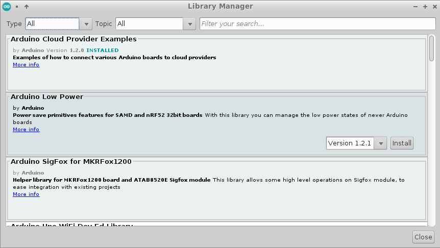
To load this, start by opening the Arduino IDE, and go to the Sketch->Include Library->Manage Libraries option on the menu
The Library Manager will now open
We need to install two (2) Libraries
– Adafruit GFX ( this is for graphics) – Adafruit SSD1306 ( to control the actual display )
Click on “Close” after installation is completed.
Using the display
We will use one of the standard Adafruit examples to show you the capabilities of the tiny little screen. The example are so straight forward to use, that I find it unnecessary to say anything else about it 🙂
Open the ssd1306_128x32_ic2 Example from the Examples menu in the Arduino IDE and upload it to your Arduino, making sure that you set the dimensions of your screen first (in my case 128×32 )
/**************************************************************************
 This is an example for our Monochrome OLEDs based on SSD1306 drivers

 Pick one up today in the adafruit shop!
 ------> http://www.adafruit.com/category/63_98

 This example is for a 128x32 pixel display using I2C to communicate
 3 pins are required to interface (two I2C and one reset).

 Adafruit invests time and resources providing this open
 source code, please support Adafruit and open-source
 hardware by purchasing products from Adafruit!

 Written by Limor Fried/Ladyada for Adafruit Industries,
 with contributions from the open source community.
 BSD license, check license.txt for more information
 All text above, and the splash screen below must be
 included in any redistribution.
 **************************************************************************/

#include <SPI.h>
#include <Wire.h>
#include <Adafruit_GFX.h>
#include <Adafruit_SSD1306.h>

#define SCREEN_WIDTH 128 // OLED display width, in pixels
#define SCREEN_HEIGHT 32 // OLED display height, in pixels

// Declaration for an SSD1306 display connected to I2C (SDA, SCL pins)
#define OLED_RESET     4 // Reset pin # (or -1 if sharing Arduino reset pin)
Adafruit_SSD1306 display(SCREEN_WIDTH, SCREEN_HEIGHT, &Wire, OLED_RESET);

#define NUMFLAKES     10 // Number of snowflakes in the animation example

#define LOGO_HEIGHT   16
#define LOGO_WIDTH    16
static const unsigned char PROGMEM logo_bmp[] =
{ B00000000, B11000000,
  B00000001, B11000000,
  B00000001, B11000000,
  B00000011, B11100000,
  B11110011, B11100000,
  B11111110, B11111000,
  B01111110, B11111111,
  B00110011, B10011111,
  B00011111, B11111100,
  B00001101, B01110000,
  B00011011, B10100000,
  B00111111, B11100000,
  B00111111, B11110000,
  B01111100, B11110000,
  B01110000, B01110000,
  B00000000, B00110000 };

void setup() {
  Serial.begin(9600);

  // SSD1306_SWITCHCAPVCC = generate display voltage from 3.3V internally
  if(!display.begin(SSD1306_SWITCHCAPVCC, 0x3C)) { // Address 0x3C for 128x32
    Serial.println(F("SSD1306 allocation failed"));
    for(;;); // Don't proceed, loop forever
  }

  // Show initial display buffer contents on the screen --
  // the library initializes this with an Adafruit splash screen.
  display.display();
  delay(2000); // Pause for 2 seconds

  // Clear the buffer
  display.clearDisplay();

  // Draw a single pixel in white
  display.drawPixel(10, 10, SSD1306_WHITE);

  // Show the display buffer on the screen. You MUST call display() after
  // drawing commands to make them visible on screen!
  display.display();
  delay(2000);
  // display.display() is NOT necessary after every single drawing command,
  // unless that's what you want...rather, you can batch up a bunch of
  // drawing operations and then update the screen all at once by calling
  // display.display(). These examples demonstrate both approaches...

  testdrawline();      // Draw many lines

  testdrawrect();      // Draw rectangles (outlines)

  testfillrect();      // Draw rectangles (filled)

  testdrawcircle();    // Draw circles (outlines)

  testfillcircle();    // Draw circles (filled)

  testdrawroundrect(); // Draw rounded rectangles (outlines)

  testfillroundrect(); // Draw rounded rectangles (filled)

  testdrawtriangle();  // Draw triangles (outlines)

  testfilltriangle();  // Draw triangles (filled)

  testdrawchar();      // Draw characters of the default font

  testdrawstyles();    // Draw 'stylized' characters

  testscrolltext();    // Draw scrolling text

  testdrawbitmap();    // Draw a small bitmap image

  // Invert and restore display, pausing in-between
  display.invertDisplay(true);
  delay(1000);
  display.invertDisplay(false);
  delay(1000);

  testanimate(logo_bmp, LOGO_WIDTH, LOGO_HEIGHT); // Animate bitmaps
}

void loop() {
}

void testdrawline() {
  int16_t i;

  display.clearDisplay(); // Clear display buffer

  for(i=0; i<display.width(); i+=4) {
    display.drawLine(0, 0, i, display.height()-1, SSD1306_WHITE);
    display.display(); // Update screen with each newly-drawn line
    delay(1);
  }
  for(i=0; i<display.height(); i+=4) {
    display.drawLine(0, 0, display.width()-1, i, SSD1306_WHITE);
    display.display();
    delay(1);
  }
  delay(250);

  display.clearDisplay();

  for(i=0; i<display.width(); i+=4) {
    display.drawLine(0, display.height()-1, i, 0, SSD1306_WHITE);
    display.display();
    delay(1);
  }
  for(i=display.height()-1; i>=0; i-=4) {
    display.drawLine(0, display.height()-1, display.width()-1, i, SSD1306_WHITE);
    display.display();
    delay(1);
  }
  delay(250);

  display.clearDisplay();

  for(i=display.width()-1; i>=0; i-=4) {
    display.drawLine(display.width()-1, display.height()-1, i, 0, SSD1306_WHITE);
    display.display();
    delay(1);
  }
  for(i=display.height()-1; i>=0; i-=4) {
    display.drawLine(display.width()-1, display.height()-1, 0, i, SSD1306_WHITE);
    display.display();
    delay(1);
  }
  delay(250);

  display.clearDisplay();

  for(i=0; i<display.height(); i+=4) {
    display.drawLine(display.width()-1, 0, 0, i, SSD1306_WHITE);
    display.display();
    delay(1);
  }
  for(i=0; i<display.width(); i+=4) {
    display.drawLine(display.width()-1, 0, i, display.height()-1, SSD1306_WHITE);
    display.display();
    delay(1);
  }

  delay(2000); // Pause for 2 seconds
}

void testdrawrect(void) {
  display.clearDisplay();

  for(int16_t i=0; i<display.height()/2; i+=2) {
    display.drawRect(i, i, display.width()-2*i, display.height()-2*i, SSD1306_WHITE);
    display.display(); // Update screen with each newly-drawn rectangle
    delay(1);
  }

  delay(2000);
}

void testfillrect(void) {
  display.clearDisplay();

  for(int16_t i=0; i<display.height()/2; i+=3) {
    // The INVERSE color is used so rectangles alternate white/black
    display.fillRect(i, i, display.width()-i*2, display.height()-i*2, SSD1306_INVERSE);
    display.display(); // Update screen with each newly-drawn rectangle
    delay(1);
  }

  delay(2000);
}

void testdrawcircle(void) {
  display.clearDisplay();

  for(int16_t i=0; i<max(display.width(),display.height())/2; i+=2) {
    display.drawCircle(display.width()/2, display.height()/2, i, SSD1306_WHITE);
    display.display();
    delay(1);
  }

  delay(2000);
}

void testfillcircle(void) {
  display.clearDisplay();

  for(int16_t i=max(display.width(),display.height())/2; i>0; i-=3) {
    // The INVERSE color is used so circles alternate white/black
    display.fillCircle(display.width() / 2, display.height() / 2, i, SSD1306_INVERSE);
    display.display(); // Update screen with each newly-drawn circle
    delay(1);
  }

  delay(2000);
}

void testdrawroundrect(void) {
  display.clearDisplay();

  for(int16_t i=0; i<display.height()/2-2; i+=2) {
    display.drawRoundRect(i, i, display.width()-2*i, display.height()-2*i,
      display.height()/4, SSD1306_WHITE);
    display.display();
    delay(1);
  }

  delay(2000);
}

void testfillroundrect(void) {
  display.clearDisplay();

  for(int16_t i=0; i<display.height()/2-2; i+=2) {
    // The INVERSE color is used so round-rects alternate white/black
    display.fillRoundRect(i, i, display.width()-2*i, display.height()-2*i,
      display.height()/4, SSD1306_INVERSE);
    display.display();
    delay(1);
  }

  delay(2000);
}

void testdrawtriangle(void) {
  display.clearDisplay();

  for(int16_t i=0; i<max(display.width(),display.height())/2; i+=5) {
    display.drawTriangle(
      display.width()/2  , display.height()/2-i,
      display.width()/2-i, display.height()/2+i,
      display.width()/2+i, display.height()/2+i, SSD1306_WHITE);
    display.display();
    delay(1);
  }

  delay(2000);
}

void testfilltriangle(void) {
  display.clearDisplay();

  for(int16_t i=max(display.width(),display.height())/2; i>0; i-=5) {
    // The INVERSE color is used so triangles alternate white/black
    display.fillTriangle(
      display.width()/2  , display.height()/2-i,
      display.width()/2-i, display.height()/2+i,
      display.width()/2+i, display.height()/2+i, SSD1306_INVERSE);
    display.display();
    delay(1);
  }

  delay(2000);
}

void testdrawchar(void) {
  display.clearDisplay();

  display.setTextSize(1);      // Normal 1:1 pixel scale
  display.setTextColor(SSD1306_WHITE); // Draw white text
  display.setCursor(0, 0);     // Start at top-left corner
  display.cp437(true);         // Use full 256 char 'Code Page 437' font

  // Not all the characters will fit on the display. This is normal.
  // Library will draw what it can and the rest will be clipped.
  for(int16_t i=0; i<256; i++) {
    if(i == '\n') display.write(' ');
    else          display.write(i);
  }

  display.display();
  delay(2000);
}

void testdrawstyles(void) {
  display.clearDisplay();

  display.setTextSize(1);             // Normal 1:1 pixel scale
  display.setTextColor(SSD1306_WHITE);        // Draw white text
  display.setCursor(0,0);             // Start at top-left corner
  display.println(F("Hello, world!"));

  display.setTextColor(SSD1306_BLACK, SSD1306_WHITE); // Draw 'inverse' text
  display.println(3.141592);

  display.setTextSize(2);             // Draw 2X-scale text
  display.setTextColor(SSD1306_WHITE);
  display.print(F("0x")); display.println(0xDEADBEEF, HEX);

  display.display();
  delay(2000);
}

void testscrolltext(void) {
  display.clearDisplay();

  display.setTextSize(2); // Draw 2X-scale text
  display.setTextColor(SSD1306_WHITE);
  display.setCursor(10, 0);
  display.println(F("scroll"));
  display.display();      // Show initial text
  delay(100);

  // Scroll in various directions, pausing in-between:
  display.startscrollright(0x00, 0x0F);
  delay(2000);
  display.stopscroll();
  delay(1000);
  display.startscrollleft(0x00, 0x0F);
  delay(2000);
  display.stopscroll();
  delay(1000);
  display.startscrolldiagright(0x00, 0x07);
  delay(2000);
  display.startscrolldiagleft(0x00, 0x07);
  delay(2000);
  display.stopscroll();
  delay(1000);
}

void testdrawbitmap(void) {
  display.clearDisplay();

  display.drawBitmap(
    (display.width()  - LOGO_WIDTH ) / 2,
    (display.height() - LOGO_HEIGHT) / 2,
    logo_bmp, LOGO_WIDTH, LOGO_HEIGHT, 1);
  display.display();
  delay(1000);
}

#define XPOS   0 // Indexes into the 'icons' array in function below
#define YPOS   1
#define DELTAY 2

void testanimate(const uint8_t *bitmap, uint8_t w, uint8_t h) {
  int8_t f, icons[NUMFLAKES][3];

  // Initialize 'snowflake' positions
  for(f=0; f< NUMFLAKES; f++) {
    icons[f][XPOS]   = random(1 - LOGO_WIDTH, display.width());
    icons[f][YPOS]   = -LOGO_HEIGHT;
    icons[f][DELTAY] = random(1, 6);
    Serial.print(F("x: "));
    Serial.print(icons[f][XPOS], DEC);
    Serial.print(F(" y: "));
    Serial.print(icons[f][YPOS], DEC);
    Serial.print(F(" dy: "));
    Serial.println(icons[f][DELTAY], DEC);
  }

  for(;;) { // Loop forever...
    display.clearDisplay(); // Clear the display buffer

    // Draw each snowflake:
    for(f=0; f< NUMFLAKES; f++) {
      display.drawBitmap(icons[f][XPOS], icons[f][YPOS], bitmap, w, h, SSD1306_WHITE);
    }

    display.display(); // Show the display buffer on the screen
    delay(200);        // Pause for 1/10 second

    // Then update coordinates of each flake...
    for(f=0; f< NUMFLAKES; f++) {
      icons[f][YPOS] += icons[f][DELTAY];
      // If snowflake is off the bottom of the screen...
      if (icons[f][YPOS] >= display.height()) {
        // Reinitialize to a random position, just off the top
        icons[f][XPOS]   = random(1 - LOGO_WIDTH, display.width());
        icons[f][YPOS]   = -LOGO_HEIGHT;
        icons[f][DELTAY] = random(1, 6);
      }
    }
  }
}
I hope that you find this useful and inspiring. Thank you
In this post, I will tell you all the basics of the I2C protocol. What it is, where it comes from and also how it is configured and setup. We will also look at how data is transferred and received
I2C communication is the short form name for inter-integrated circuit protocol. It is a communication protocol developed by Philips Semiconductors for the transfer of data between a central processor and multiple integrated circuits on the same circuit board by using just two common wires.
Due to its simplicity, it is widely adopted for communication between microcontrollers and sensor arrays, displays, IoT devices, EEPROMs etc.
This is a synchronous serial communication protocol. It means that data bits are transferred one by one at regular intervals of time set by a reference clock line.
The Features of I2C
The I2C protocol has the following important features
Only two common bus lines (wires) are required to control any device/IC on the I2C network.
There is no need for a prior agreement on data transfer rate like in UART communications. The data transfer speed can thus be adjusted whenever it is required.
It has a simple mechanism for validating the transferred data.
It uses a 7-bit addressing system to target a specific device/IC on the I2C bus.
I2C networks are extremely easy to scale. New devices can simply be connected to the two common I2C bus lines.
The Hardware
The physical I2C Bus
The I2C Bus (Interface wires) consists of just two wires and are named Serial Clock Line (SCL) and Serial Data Line (SDA). The data to be transferred is sent through the SDA wire and is synchronized with the clock signal from SCL. All the devices/ICs on the I2C network are connected to the same SCL and SDA lines as shown in the image below:
The physical I2C Bus. All devices are connected to the same 2 wired on the bus, namely SDA and SCL
Both the I2C bus lines (SDA, SCL) are operated as in open-drain driver mode. It means that any device/IC on the I2C network can drive(pull) SDA and SCL low, but they cannot drive them high. So, a pull-up resistor is used on each bus line, to keep them high (at positive voltage) by default.
This is to prevent the bus from shorting, which might happen when one device tries to pull the line high and some other device tries to pull the line low.
The Master and Slave Devices on the I2C Bus
The devices connected to the I2C bus are categorized as either masters or slaves. At any instant of time, only a single master stays active on the I2C bus. It controls the SCL clock line and decides what operation is to be done on the SDA data line.
All the devices that respond to instructions from this master device are slaves. For differentiating between multiple slave devices connected to the same I2C bus, each slave device is physically assigned a permanent 7-bit address.
When a master device wants to transfer data to or from a slave device, it specifies this particular slave device address on the SDA line and then proceeds with the transfer. So effectively communication takes place between the master device and a particular slave device.
All the other slave devices don’t respond unless their address is specified by the master device on the SDA line.
The Master and Slave Devices on the I2C Bus. Note that each Slave device has it’s own address.
The Data Transfer Protocol
The protocol (set of rules) that is followed by the master device and slave devices for the transfer of data between them works as follows:
Data is transferred between the master device and slave devices through the SDA data line, via patterned sequences of 0’s and 1’s (bits). Each sequence of 0’s and 1’s is called a transaction and each data transaction is structured as in the image below:
The structure of an I2C Data transaction
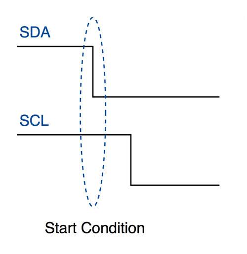
The Start Condition
Whenever a master device/IC decides to start a transaction, it switches the SDA line from a high level to a low level before the SCL line switches from high to low.
Once a start condition is sent by the master device, all the slave devices get active even if they were in sleep mode, and wait for the address bits to see which device should respond.
The I2C Start Condition. Note that SDA Switches LOW before SCL. All slave devices on the bus will now listen for an address bit to decide which device should respond.
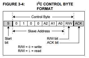
The Address Block
The Address block is comprised of 7 bits and are filled with the address of slave device (in binary) to/from which the master device needs to send/receive data. All the slave devices on the I2C bus will compare these address bits with their own address.
The Read/Write Bit
This bit specifies the direction that the data must be transferred in. If the master device/IC needs to send data to a slave device, this bit is set to ‘0’. If the master device/IC needs to receive data from the slave device, it is set to ‘1’.
The ACK/NACK Bit
This is the Acknowledged/Not-Acknowledged bit. If the physical address of any slave device is the same as the address that was broadcasted by the master device, that slave device will set the value of this bit to ‘0’ . If there are no slave device(s) with the broadcasted address, this bit will remain at logic ‘1’ (default). This will tell the master that the data/command has been received and/or acknowledged by a slave device.
The Data Block
The data block is comprised of 8 bits and they are set by the transmitter,wheather this be the master or the slave, depending on wheather a read or a write operation was requested, with the data bits that needs to transfered to the receiver. This block is followed by an ACK/NACK bit that is set to ‘0’ by the receiver if it successfully receives data. Otherwise it stays at logic ‘1’.
This combination of data blocks followed by an ACK/NACK bit is repeated until all the data is completely transferred.
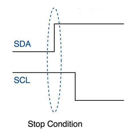
The Stop Condition
After all the required data blocks are transferred through the SDA line, the master device switches the SDA line from low to high before the SCL line switches back from high to low.
The I2C Stop condition. This signals the end of a transaction. Note SDA returns to High BEFORE the SCL line is pulled High.
How does I2C work in practice
When an I2C transaction is initiated by a master device either to send or receive data to/from a slave device, all of the processes mentioned above will happen at least one. Let us look at a typical scenario for each of the different type of scenarios.
Sending Data to a Slave Device
The following sequence of operations will take place when a master device tries to send data to a particular slave device through I2C bus:
The master device sends a start condition
The master device sends the 7 address bits which correspond to the slave device to be targeted
The master device sets the Read/Write bit to ‘0’, which signifies a write
Now two scenarios are possible:
If no slave device matches with the address sent by the master device, the next ACK/NACK bit stays at ‘1’ (default). This signals the master device that the slave device identification is unsuccessful. The master clock will end the current transaction by sending a Stop condition or a new Start condition
If a slave device exists with the same address as the one specified by the master device, the slave device sets the ACK/NACK bit to ‘0’, which signals the master device that a slave device is successfully targeted
If a slave device is successfully targeted, the master device now sends 8 bits of data which is only considered and received by the targeted slave device. This data means nothing to the remaining slave devices
If the data is successfully received by the slave device, it sets the ACK/NACK bit to ‘0’, which signals the master device to continue
The previous two steps are repeated until all the data is transferred
After all the data is sent to the slave device, the master device sends the Stop condition which signals all the slave devices that the current transaction has ended
The image below represents the transaction with the data bits sent on the SDA line and the device that controls each of them:
I2C Master sending data to a slave device
Reading Data from a Slave Device
The sequence of operations remain the same as in previous scenario except for the following:
The master device sets the Read/Write bit to ‘1’ instead of ‘0’ which signals the targeted slave device that the master device is expecting data from it
The 8 bits corresponding to the data block are sent by the slave device and the ACK/NACK bit is set by the master device
Once the required data is received by the master device, it sends a NACK bit. Then the slave device stops sending data and releases the SDA line
If the master device to read data from specific internal location of a slave device, it first sends the location data to the slave device using the steps in previous scenario. It then starts the process of reading data with a repeated start condition.
The below figure represents the overall data bits sent on the SDA line and the device that controls each of them:
Reading data from a Slave device on the I2C bus
The Clock Stretching concept
Let say the master device started a transaction and sent address bits of a particular slave device followed by a Read bit of ‘1’. The specific slave device needs to send an ACK bit, immediately followed by data.
But if the slave device needs some time to fetch and send data to master device, during this gap, the master device will think that the slave device is sending some data.
To prevent this, the slave device holds the SCL clock line low until it is ready to transfer data bits. By doing this, the slave device signals the master device to wait for data bits until the clock line is released
Conclusion
This concludes this tutorial. In a future post, I will show you how to use I2C to transfer data between two micro-controllers.
You are excited, you have just finished your new IoT device, and have many excellent ideas on how you will use it remotely, on your smartphone, or even from your computer at the office. You now start thinking about how you will send and receive data to this new device of yours…
There are many ways that you can do this, but today, I would like to suggest a very easy and lightweight data transfer protocol. It is called MQTT. Some of you may already be using it, or you may at least have heard about it. Read on if you would like to know more about what it is, as well as how it works.
The History of MQTT
MQTT was designed by Andy Stanford-Clark (IBM) and Arlen Nipper (Cirrus Link, then Eurotech) in 1999. It was first used to monitor an oil pipeline running through the desert. The goal was to design and implement a protocol that is bandwidth-efficient, lightweight and uses very little battery power, because the devices were connected via satellite link which, at that time, was extremely expensive.
In 2013, IBM submitted the MQTT v3.1 protocol to the OASIS specification body with a charter that ensured that only minor changes to the specification could be accepted.MQTT-SN is a variation of the main protocol aimed at embedded devices on non-TCP/IP networks, such as Zigbee.
Historically, the “MQ” in “MQTT” came from the IBM MQ (then ‘MQSeries’) MQ product line. The protocol, however, provides publish-and-subscribe messaging (no queues, in spite of the name) and was specifically designed for resource-constrained devices and low bandwidth, high latency networks. This makes it an excellent candidate for data transmission on IoT and other low resource devices.
The Protocol Architecture (How does it work)
MQTT uses a client-server architecture, where the server is called the broker, and the client, called a client. The broker typically functions like a post office, in the sense that it doesn’t use the client’s address, but rather the subject of the topic that a client is subscribed to, to determine which client should receive a certain message.
This enables many clients to subscribe to the same subject, with each receiving the same message. Clients can also publish a topic, thus transmitting or sending a message to other clients. This concept make bidirectional communication possible between clients, and it also ensures that it is extremely easy to use.
What do theses topics look like?
An MQTT Topic is a text string, delimited by a / for example, let us say you have a device in your kitchen, that monitors the temperature, and controls the lights and microwave oven.
This device may use the following topics to publish (send data) or subscribe to (receive data)
As you can see, we can easily group topics by their location. It would thus be very easy for a smart home controller, like OpenHab or similar to get status or set a particular state in a certain room or area.
This can be done by using wildcard operators, of which there are two, the + and #
If we want to subscribe to all the lights in the house, we can subscribe to the following topic:
@msg/myhouse/+/lights
This will give us the data from the following topics: @msg/myhouse/kitchen/lights @msg/myhouse/livingroom/lights @msg/myhouse/bedroom/lights
You can also subscribe to a multilevel wildcard topic, for example:
@msg/myhouse/kitchen/#
This will subscribe you to all the topics related to the kitchen.
How do I get access to MQTT
There are quite a few online MQTT brokers available that allow you to apply for a free account. These services have many limits on the amounts of messages you may send or receive, but generally, they are quite useful.
Adafruit.io should be well known. It is stable, and easy to use. They do however have a few limitations on how many devices and messages you can add to the service.
NetPie.io is a fairly unknown provider outside of Thailand. They limit you to 3 Projects, with 10 devices per project, but their messaging limits are extremely liberal and permissive. This service will also always be free (or at least that is according to NetPie themselves). On the negative side, all the configuration is available in English, but all the documentation is in Thai. You can however use Google Translate to translate it into a language that you can understand.
If you are not comfortable with running your data on an online broker, you can also download and install one of the many MQTT brokers that are available for installation on Linux and MS-Windows. This will, however, mean that you should also have permanent Internet access, as well as a public IP address, to enable your devices to connect to your broker.
Microprocessor and other Device support
MQTT Libraries are available for use on Arduino, STM32, ESP32 as well as Raspberry PI and Python. You can also get clients and brokers for the Linux and MS-Windows platforms.
Smartphone Access
Various applications exist on the google playstore, as well as the Apple App Store, that allow you to connect to an MQTT broker, subscribe to topics, and also publish topics. Many of these are free to use, and also provide you with a nice user interface.
You can also write your own smartphone app, if you are skilled enough, to do exactly what you want it do do.