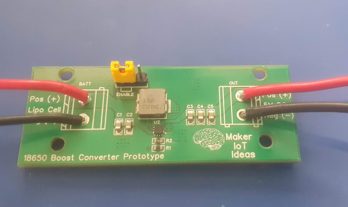
As part of an ongoing project, this tiny boost converter was designed to be used to power some of my projects, as well as become a part of a much-needed add-on circuit to the single-cell 18650 charger PCB that I designed a while ago.
I received a lot of very useful comments from readers about the circuit below ( the single-cell 18560 Lipo charger). Most of these comments were related to adding a boost converter to the circuit, to add a little more versatility to the circuit.
I never just add something though, and as such, this boost converter prototype was designed to test out the components and design before incorporating it into the main design. That way, I can iron out any problems before adding it to a bigger circuit.
The boost converter is based on the MP3423GG-Z, from MPS. I have decided to stay very close to their recommended application notes, so the circuit is stock standard. Another way to ensure that performance is what I want it to be, and also, to be frank, because I don’t believe I need to make any changes to the manufacturer-recommended circuit.
Some other comments suggested the use of “ideal diodes” at the output , in order to be able to daisy-chain the chargers. That will be addressed in a later post this month, as I am also currently testing out one of the many “ideal diode” integrated circuit chips available – in this case the MAX40200.
Being a “prototype” I did not bother with adding proper connectors to this version, as it will only be used for a short while. Soldering the supply and output wires directly to the PCB will thus be sufficient for the time being.
Design and Manufacturing
I choose PCBWay for my PCB manufacturing. Why? What makes them different from the rest?
PCBWay‘s business goal is to be the most professional PCB manufacturer for prototyping and low-volume production work in the world. With more than a decade in the business, they are committed to meeting the needs of their customers from different industries in terms of quality, delivery, cost-effectiveness and any other demanding requests. As one of the most experienced PCB manufacturers and SMT Assemblers in China, they pride themselves to be our (the Makers) best business partners, as well as good friends in every aspect of our PCB manufacturing needs. They strive to make our R&D work easy and hassle-free.
How do they do that?
PCBWay is NOT a broker. That means that they do all manufacturing and assembly themselves, cutting out all the middlemen, and saving us money.
PCBWay’s online quoting system gives a very detailed and accurate picture of all costs upfront, including components and assembly costs. This saves a lot of time and hassle.
PCBWay gives you one-on-one customer support, that answers you in 5 minutes ( from the Website chat ), or by email within a few hours ( from your personal account manager). Issues are really resolved very quickly, not that there are many anyway, but, as we are all human, it is nice to know that when a gremlin rears its head, you have someone to talk to who will do his/her best to resolve your issue as soon as possible.
This PCB really would benefit from having a stencil available when you assemble it by hand. The MP3423GG-Z is super tiny, so having a guide to apply just the right amount of solder paste to the pads will go a long long way to make sure that there is no reworking needed.
All of the other components are quite manageable, being only a couple of 0805 and 0603 resistors, and an inductor. I reflow soldered everything at the same time with a hotplate. It is worth noting that I did have to remove and replace the MP3423GG-Z once during the reflow process… tiny solder bridges formed between some pins, but carefully lifting it up with a pair of tweezers, and placing it onto the pads again got rid of those completely.
We may be tempted to “leave it off the board, wait for the solder to flow and then place the component onto the molten solder…” I am not too sure about the thermal stresses that that method may or may not induce in the component… so, I prefer having it heat up slowly with the rest of the components/ and then make a quick adjustment if needed… Comments on this anyone?
Testing and final thoughts
Testing the boost converter went without any problems. It delivers a stable 5.15v DC at the output, from an input voltage of 3.3v to 4.2v. I did not test it lower than that yet… Current output seems quite stable, and the voltage does not fluctuate under load ( I tested with 2 LED COB lights, each drawing 600mA, connected in series – thus 1.2A — That is definitely the maximum current that I intend to draw from this device, although it is rated at 3A
Ripple current seems to be within the 100mV stated in the datasheet.
In summary, I believe the device performs the intended duty that i set out to design. The assembly is a bit tricky due to the small size of the MP3423GG-Z, as well as my “not-so-good” eyesight. All that aside, I am ready to advance to the next phase of the overall project – revision 2 of the Single Cell 18650 Lipo Charger.
This is a Simple IoT Plant Watering Solution, done as another collaboration with the local High School in my Area. In this project, they took a group of purely academic students ( Language majors ) and told them that they had to design an electronics project that would have use in the real world…
This presented a very tough situation to the students since they had never even imagined that they could do something like this… (Think along the lines of a Senior Design project, like what you would give EE Students during their final year – with all the documentation, pamphlets, and explanations – i.e. lots and lots of paperwork) , and then also add on the requirement that they had to present a practical project as well! And they have only 45 days to do that as well!
I came into this picture late on a Thursday or Friday afternoon, with a group of students milling around outside the Electronics lab. They were unknown to me and seemed quite flustered… I invited them in, and eventually, they started opening up about their problem…
As it turned out, they were completely clueless, and did not know where to start with anything, not even what they wanted to do! Their initial idea went like “something that uses a camera to sort garbage by type and material” – that was never going to happen, not in 45 days, and not with the allocated budget of no more than $USD30.00 they were allowed. Lets not even go to the machine learning stuff, training of the models etc…
So, I took over, and decided that we shall do a simple IoT Plant Watering Solution. It is complex enough for Grade 11 students, and more importantly, I knew that I could teach them enough Arduino coding and basic electronics skills in the time allotted to get the project completed successfully.
What followed was a few very intensive sessions after school to get the paperwork sorted. For some reason, their teacher required ALL paperwork be completed upfront, with the entire design and code prepared before they touched the practical stuff – A funny way to design stuff if you ask me, but that is how we did it…
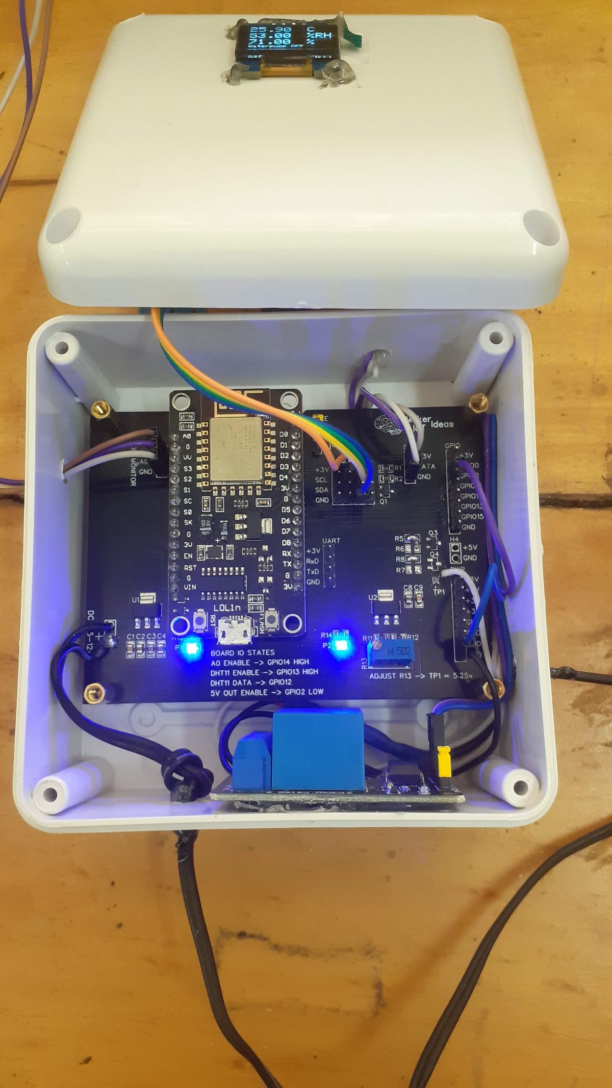
We settled on the ESP8266 12-E NodeMCU v3 development board, A resistive soil sensor, a DHT11 for temperature and humidity data, a small OLED I2C display and a small 5v USB-powered water pump. While they ordered the components, we started with basic coding classes, and this is where the story changes.
These kids blew me away with their level of interest, their attitude to learning, and how quickly they grasped the concepts. In no time at all, they were coding basic sketches, taking readings, learning how the different sensors worked, and pushing the envelope by adding lots more complementary components like MOSFETs and BJT transistors.
With this level of enthusiasm, I could not help but also become very excited, and thus decided to go a bit further than usual and help them design a neat PCB baseboard for the NodeMCU. That way, we could get rid of all those pesky wire connections, and maybe even produce something that looked good.
This is what we came up with, here shown just after SMD component placing. They ( the students ) did all of that by themselves as well, and it turned out to be a lot of fun for them, with some funny moments for me as well.
The Assembly ( First time ever )
The PCB, together with a stencil, arrived from PCBWay on about the 15th of this month.
I choose PCBWay for my PCB manufacturing. Why? What makes them different from the rest?
PCBWay‘s business goal is to be the most professional PCB manufacturer for prototyping and low-volume production work in the world. With more than a decade in the business, they are committed to meeting the needs of their customers from different industries in terms of quality, delivery, cost-effectiveness and any other demanding requests. As one of the most experienced PCB manufacturers and SMT Assemblers in China, they pride themselves to be our (the Makers) best business partners, as well as good friends in every aspect of our PCB manufacturing needs. They strive to make our R&D work easy and hassle-free.
How do they do that?
PCBWay is NOT a broker. That means that they do all manufacturing and assembly themselves, cutting out all the middlemen, and saving us money.
PCBWay’s online quoting system gives a very detailed and accurate picture of all costs upfront, including components and assembly costs. This saves a lot of time and hassle.
PCBWay gives you one-on-one customer support, that answers you in 5 minutes ( from the Website chat ), or by email within a few hours ( from your personal account manager). Issues are really resolved very quickly, not that there are many anyway, but, as we are all human, it is nice to know that when a gremlin rears its head, you have someone to talk to who will do his/her best to resolve your issue as soon as possible.
This caused quite a lot of excitement from the students since they asked me to get to school immediately, and offered to stay after school to get the assembly done. So, I packed up all the components required, got in the car, and a few minutes later, we had an assembly line running 🙂
It took them only a few minutes to understand how to read the BOM file, use that information to find the right components and take turns to place a few components at a time onto the PCB. ( I did the solder paste and stencil thing on my own, as that could potentially turn out to be a very messy and wasteful operation if I let them do it )
During this assembly, they were quite amazed at what they were doing, but also quite confused as to how we would ” make the components stick to the PCB later”. They have seen soldering on YouTube, and could not understand how this “grey paste” could “turn hard and shiny” – with some even trying to rush their friends, as the paste would dry up and become sticky…
That signalled to me that we should get the hot air ready, and show them properly, as it would stop the speculation, and give them closure on their questions, because no matter how much I tried to explain that the solder paste would be melted later, they could not understand that concept.
Once I reflowed the first few components using hot air, they all once again took turns with a small group of components on the PCB ( We assembled 2 PCB’s to make sure everybody got a chance to try everything)
Through-hole soldering of the various header pins and other components was next. Once again, I showed them an example and then stepped back while they took over and completed the task. At this time it was about 17:30 already, so I sent them all home, with a promise to return the next day and complete the rest of the build.
Final Assembly and the Enclosure
We added some copper standoffs to the bottom of the enclosure, drilled some holes and mounted everything with screws and hot glue. The some final testing was performed, and the project was placed outside, next to a potted plant, and put on a sort of soak test, to verify operation for a few days.
A discussion of the circuit
In this circuit, I made use of a very cheap resistive soil moisture probe sensor. It consists of an etched PCB probe and a separate OPAMP on an additional PCB. This assembly then sends an analog voltage back to the Microprocessor for analysis. Very easy to use, and as mentioned, extremely cheap! But this is also a big problem. As seen in many other posts online, people don’t like these probes, as they don’t seem to last very long, and/or become unreliable over time.
I believe that this is due to the fact that they run them continuously, and that, causes the electrodes to erode away over time – because the thing about it, you are basically running an electrolysis cell – sending voltage/current through a probe, that is suspended in a conductive medium ( the water in the soil contains minerals etc – that is why it is conductive, and why we can get a reading from it )
How do I plan to avoid this problem then? The probe is powered through a small N-Channel MOSFET. This allows us to power the probe on when we want a reading, and then power it off again. It will definitely not completely stop the electrodes eroding away over time, but I am sure it will extend the usable lifetime of the probe by quite a bit. On the downside, you need another GPIO pin to control that MOSFET, but that in itself is also a great learning opportunity
This project was extremely interesting. It was something very basic, but it gave me a very unique opportunity to teach a group of kids something they never knew before. It also initiated a spark in many of them, who are now interested in getting involved in electronics as a hobby. The possibilities of this project, if it is improved a bit more, could also be great. For example, we did not even consider adding IoT connectivity to this yet, we all decided that it was not needed, and an unnecessary complication of an already complex issue ( to the students that is). I shall keep monitoring the operation of the device over the next few weeks, and hopefully get some answers myself as to how long that soil probe will last… As a control, we have another one that was left powered on in the same container. That one are not being used to take readings, but will definitely provide us with a good comparison against the probe that is only on then used…
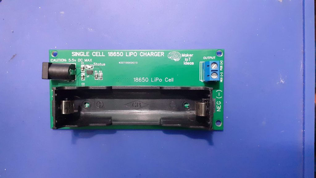
This single cell lipo charger was created to solve a problem I encountered during a recent project. I constantly needed to recharge 18650 cells, and while I could also use my 4-cell charger, that didn’t always turn out to be the most practical. I also intend to use this small charger as a building block for a future complete power solution, including a boost converter, more protection features and proper cell status indication…
I am currently moving towards building more projects that will be used outside, “in the wild” and thus need a reliable way to power those. True to my way of doing things, I want to build my own stuff as far as possible. That way, I learn more about the technology, and I am sure that everything meets my exact specifications.
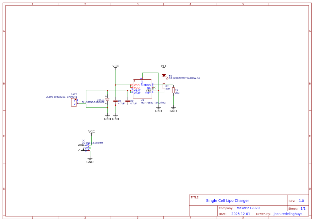
What is on the PCB?
The charger is based on the MCP73832T, by Microchip, which contains quite a lot of useful features, in a small package as well at a relatively small price tag, and with very few other required supporting components.
Linear Charge Management Controller:
Integrated Pass Transistor
Integrated Current Sense
Reverse Discharge Protection
High Accuracy Preset Voltage Regulation: + 0.75%
Four Voltage Regulation Options:
4.20V, 4.35V, 4.40V, 4.50V
Programmable Charge Current: 15 mA to 500 mA
Selectable Preconditioning:
10%, 20%, 40%, or Disable
Selectable End-of-Charge Control:
5%, 7.5%, 10%, or 20%
Charge Status Output
Tri-State Output – MCP73831
Open-Drain Output – MCP73832
Automatic Power-Down
Thermal Regulation
Temperature Range: -40°C to +85°C
Packaging:
8-Lead, 2 mm x 3 mm DFN
5-Lead, SOT-23
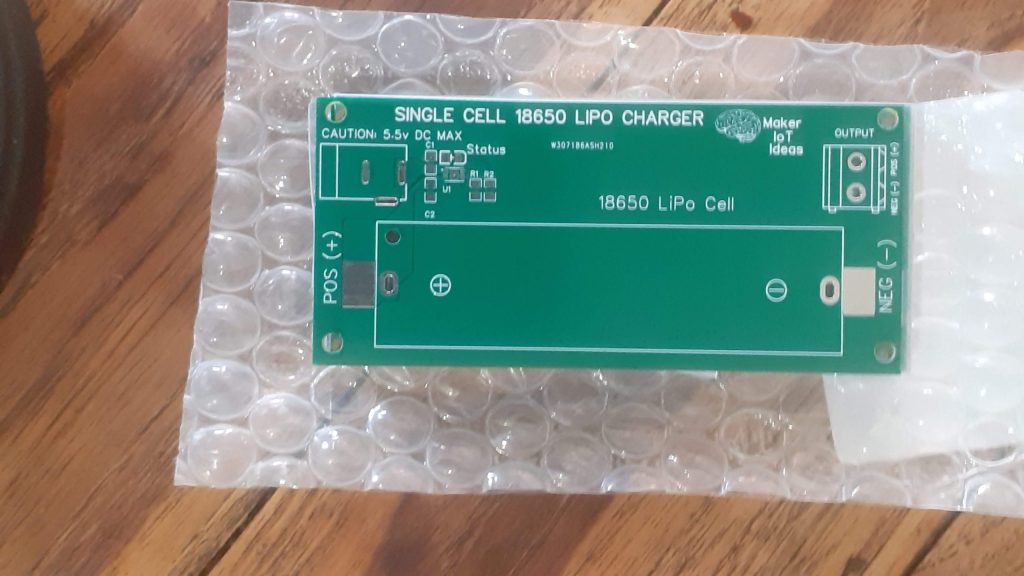
A proper screw-type connection terminal on the output, as well as a DC Barrel Jack on the input, completes the PCB. On future revisions, I will seriously consider having a voltage-limiting circuit on the input side, since the MCP73832T is only capable of accepting an input voltage of up to 5.5v DC.
This is not a problem to me, as I will be using the current version for my own personal use. I do however believe it is essential to ensure that no over-voltage conditions can accidently occur BEFORE I will give this to someone else to use.
The schematic
Manufacturing the PCB
I choose PCBWay for my PCB manufacturing. Why? What makes them different from the rest?
PCBWay‘s business goal is to be the most professional PCB manufacturer for prototyping and low-volume production work in the world. With more than a decade in the business, they are committed to meeting the needs of their customers from different industries in terms of quality, delivery, cost-effectiveness and any other demanding requests. As one of the most experienced PCB manufacturers and SMT Assemblers in China, they pride themselves to be our (the Makers) best business partners, as well as good friends in every aspect of our PCB manufacturing needs. They strive to make our R&D work easy and hassle-free.
How do they do that?
PCBWay is NOT a broker. That means that they do all manufacturing and assembly themselves, cutting out all the middlemen, and saving us money.
PCBWay’s online quoting system gives a very detailed and accurate picture of all costs upfront, including components and assembly costs. This saves a lot of time and hassle.
PCBWay gives you one-on-one customer support, that answers you in 5 minutes ( from the Website chat ), or by email within a few hours ( from your personal account manager). Issues are really resolved very quickly, not that there are many anyway, but, as we are all human, it is nice to know that when a gremlin rears its head, you have someone to talk to who will do his/her best to resolve your issue as soon as possible.
Assembly of this PCB was quite easy, providing that you have a stencil, it will not take you more than a few minutes.
The PCB’s really came out very nicely 🙂
I have also made provision for using a through-hole 18650 battery holder, just in case you are like me, and have a few lying around in a drawer, or could just not be bothered with using the SMD version…
The completed PCB is relatively small and compact, taking into consideration the size of the 18650 cell of course… The screw terminal on the output really helps to keep everything secure when using the module to power a project, and the DC barrel jack provides a good connection to charge it all back up again… Now, If I just remembered to add some form of voltage limiting on the input, as well as include a boost converter, It would be the perfect little “power bank” project… For now though, let’s leave those features to the future, as this is already extremely useful as is.
I designed this breakout to assist me during prototyping my next version of the “RP2040 Emergency Mouse“. In that project, I used the SEEED Studio Xiao RP2040, along with a few other components to create a simple but effective computer mouse-type device.
While the “mouse” works quite well, I have quite early on discovered that it could be better. More on that in a follow-up article, but let us just say that I needed more GPIO pins than that were available on the XIAO RP2040 and that the layout can be improved a bit – especially If I want to get it into an enclosure.
I am still quite neutral about CircuitPython and Micropython on microcontrollers, and Python in general, but since the above-mentioned project runs completely on CircuitPython, it made a lot of good sense to get more into it.
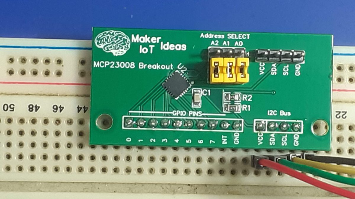
What is on the PCB?
I wanted something as small as possible, and that meant that I chose a QFN package for the MCP23008 IO expander chip. At only 4mm x 4mm, and not being bothered to try and find a DIP version, a breakout board became a much-needed necessity.
Address Selection Jumpers, Two I2C bus headers, and of course the all-important GPIO pins make up all of the user accessible interfacing. Note that the chip reset line is permanently tied to Vcc to make things a bit less cluttered, and easier to use while prototyping.
A decoupling capacitor, as well as pullup resistors on the I2c lines, were also included. Another note here, I did not provide my usual selection jumper to disable these on this particular board.
The Schematic
Manufacturing the PCB
I choose PCBWay for my PCB manufacturing. Why? What makes them different from the rest?
PCBWay‘s business goal is to be the most professional PCB manufacturer for prototyping and low-volume production work in the world. With more than a decade in the business, they are committed to meeting the needs of their customers from different industries in terms of quality, delivery, cost-effectiveness and any other demanding requests. As one of the most experienced PCB manufacturers and SMT Assemblers in China, they pride themselves to be our (the Makers) best business partners, as well as good friends in every aspect of our PCB manufacturing needs. They strive to make our R&D work easy and hassle-free.
How do they do that?
PCBWay is NOT a broker. That means that they do all manufacturing and assembly themselves, cutting out all the middlemen, and saving us money.
PCBWay’s online quoting system gives a very detailed and accurate picture of all costs upfront, including components and assembly costs. This saves a lot of time and hassle.
PCBWay gives you one-on-one customer support, that answers you in 5 minutes ( from the Website chat ), or by email within a few hours ( from your personal account manager). Issues are really resolved very quickly, not that there are many anyway, but, as we are all human, it is nice to know that when a gremlin rears its head, you have someone to talk to that will do his/her best to resolve your issue as soon as possible.
Due to the small size of the QFN package, I strongly recommend that you either have this assembled professionally, or at least consider buying a stencil for applying the solder paste to this board. Maybe those with excellent eyesight can do without that?
Assembly took only a few minutes, with the help of an extremely accurate stencil, followed by a few minutes on a hotplate, and manually soldering on the header pins.
Using the MCP23008 with CircuitPython
I2C devices are very easy to use with the Arduino IDE or similar, and as such, I will not be covering that here.
Circuitpython, however, is gaining popularity, and I am slowly starting to see what the hype is about myself…
So, to get started, you need a microcontroller running CircuitPython – See Adafruit for excellent tutorials. You will also need a few libraries from Adafruit See this link
I will give a very simple example below, showing how to set a pin as an output, as well as an input with internal pullup resistors enabled. Note that the MCP23008 DOES NOT SUPPORT pull-down resistors internally. You need to add those by yourself externally.
# Initialising all the required libraries
import board
import busio
from digitalio import Direction
from adafruit_mcp230xx.mcp23008 import MCP23008
i2c = busio.I2C(board.SCL, board.SDA)
# Adding the MCP23008
mcp = MCP23008(i2c)
# This assumes that you are using the default address [ i.e. all address
# pins are grounded]
#
#
#
# Defining two outputs on pins 0 and 1
pin0 = mcp.get_pin(0)
pin0.direction = Direction.OUTPUT
pin1 = mcp.get_pin(1)
pin1.direction = Direction.OUTPUT
#
#
# We can now control the pins by setting them to true or false, true being
# high
pin0.value = True
pin1.value = True
#
# and switch them off again by using
pin0.value = False
pin1.value = False
#
#
# We can also use the pins as inputs.
# We will activate the internal pullup as well
#
# first , we need another library
import digitalio
pin2 = mcp.get_pin(2)
pin2.direction = digitalio.Direction.INPUT
pin2.pull = digitalio.Pull.UP
#
#
# Reading the pin value is now as easy as
pin2.value
#
# This will return True if the pin is high ( its default state with pullups # activated, of False if pulled low, by for example a switch of button )
Conclusion
The breakout works as expected, and it is very easy to use with CircuitPython. I can now continue with the actual integration and Software for the RP2040 Mouse Rev 2.0 project.
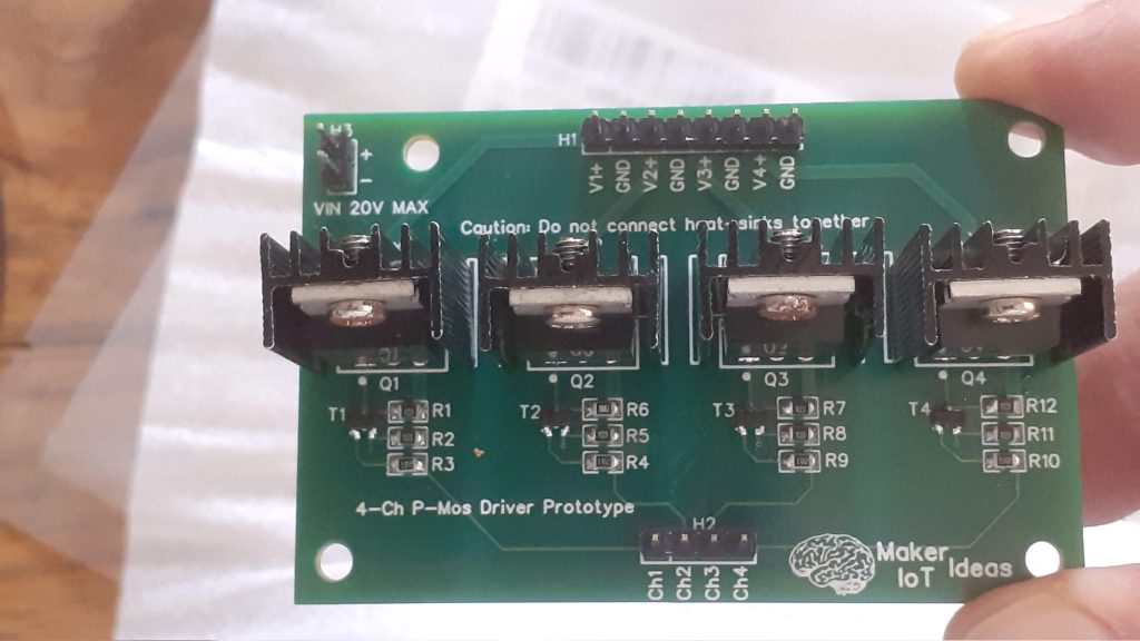
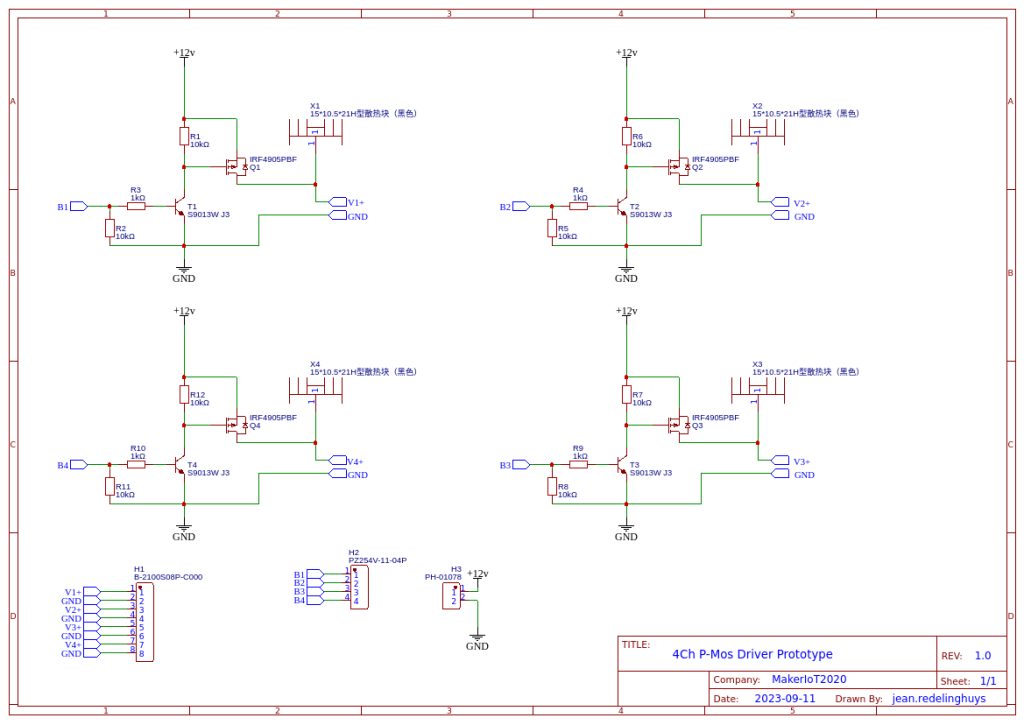
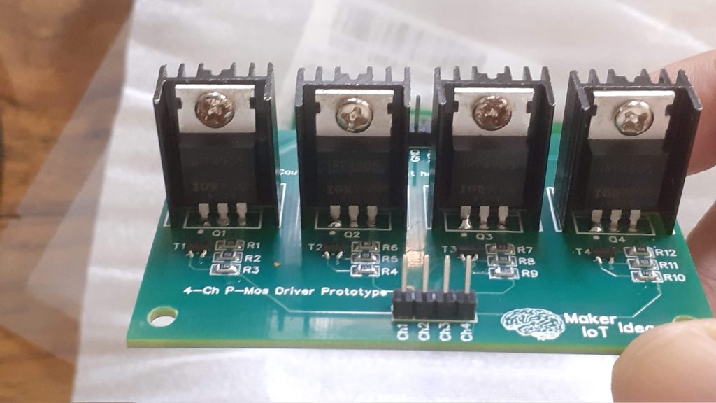
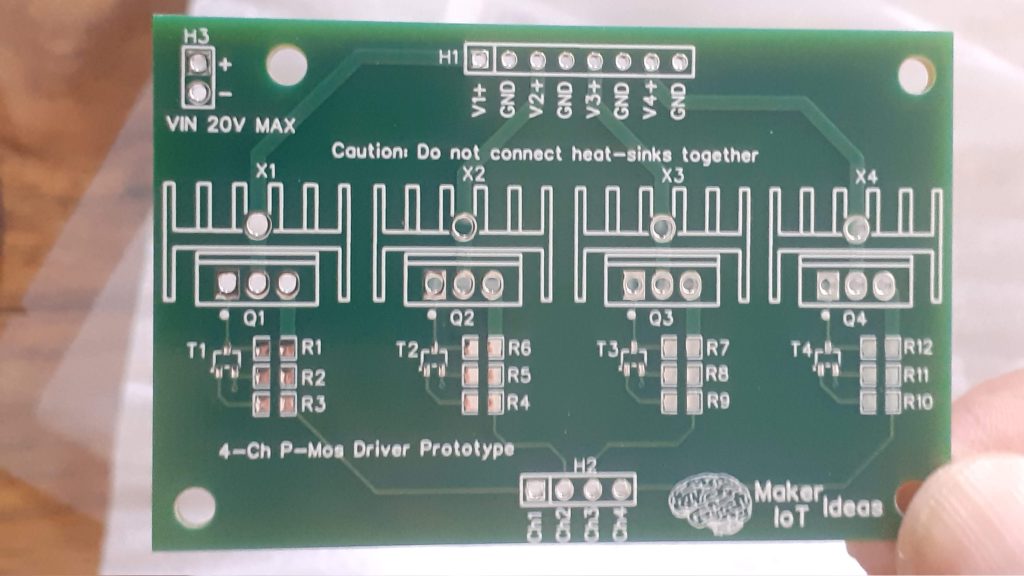
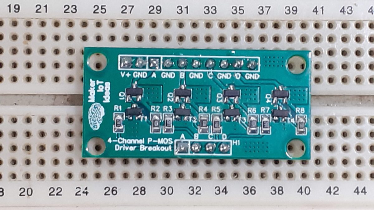
This is a modification of my existing P-MOS driver circuits, intended for use with higher current LED Lights, as well as any other applications requiring a higher current capable P-Channel Mosfet to switch a load.
What is on the PCB?
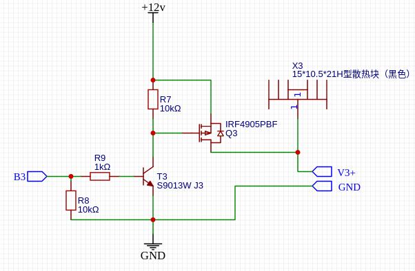
I have used the IRF4905 P-Channe Mosfet here as it can sink up to 74 Amps of current – A complete overkill in many situations. Datasheet. The Mosfet is configured in a high-side switching configuration, thus eliminating problems with ground connections.
To prevent unreliable switching, a transistor is used to switch the gate, which is normally pulled high to keep the device switched off.
I have also included various connection headers for connecting the load, Power supply, as-well-as active high control headers for controlling the driver from a microcontroller. This was especially important as the Gate voltage of the Mosfet is above the acceptable 3.3 volt for use with many of the modern microcontrollers in use today.
It is important o note that I did not yet bother to do very accurate gate current calculations. I do not need super fast switching, and on the bench, the 500mA switching capability of the S9013W transistor gave me satisfactory results.
What is my intended use for this driver?
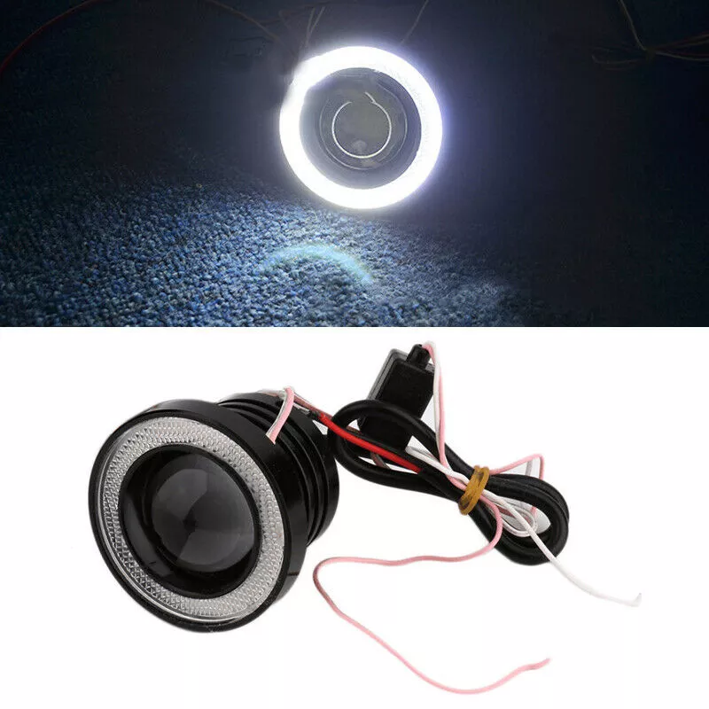
This is a 12v Automotive Fog light. It is meant to be an aftermarket upgrade. It will also be a very nice focused working light in my workshop, as the lighting is not optimal.
My initial idea is using two of these, PWM controlled from an ESPHome-controlled device to provide me with focused, dimmable lighting for assembly and other operations where a bit of extra light will be needed.
The Fish-eye lens of the internal lamp provides a very focused beam, and from initial testing seems to be exactly what I want.
The problem came in that the LED module consumes quite a bit of current ( 5A for the center lamp, and 3A for the ring light). These currents are way above the capabilities of my existing LED COB driver circuit, thus this MOD.
The Schematic
Manufacturing the PCB
I choose PCBWay for my PCB manufacturing. Why? What makes them different from the rest?
PCBWay‘s business goal is to be the most professional PCB manufacturer for prototyping and low-volume production work in the world. With more than a decade in the business, they are committed to meeting the needs of their customers from different industries in terms of quality, delivery, cost-effectiveness and any other demanding requests. As one of the most experienced PCB manufacturers and SMT Assemblers in China, they pride themselves to be our (the Makers) best business partners, as well as good friends in every aspect of our PCB manufacturing needs. They strive to make our R&D work easy and hassle-free.
How do they do that?
PCBWay is NOT a broker. That means that they do all manufacturing and assembly themselves, cutting out all the middlemen, and saving us money.
PCBWay’s online quoting system gives a very detailed and accurate picture of all costs upfront, including components and assembly costs. This saves a lot of time and hassle.
PCBWay gives you one-on-one customer support, that answers you in 5 minutes ( from the Website chat ), or by email within a few hours ( from your personal account manager). Issues are really resolved very quickly, not that there are many anyway, but, as we are all human, it is nice to know that when a gremlin rears its head, you have someone to talk to that will do his/her best to resolve your issue as soon as possible.
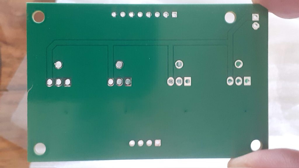
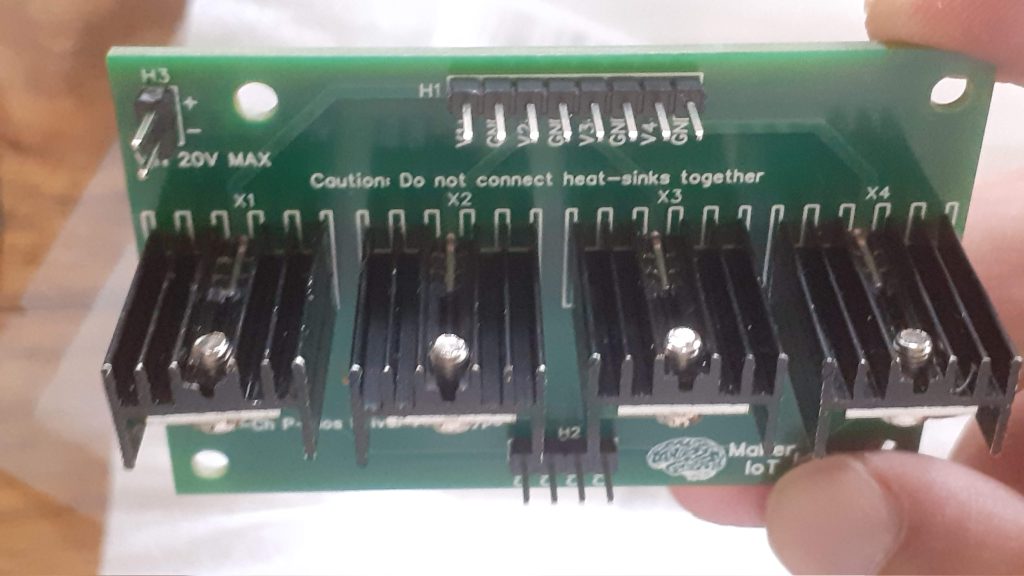
This PCB is definitely quite easy to assemble, as there are only 16 SMD components on the board. These are all easily hand-solderable. The Mosfets and their respective heatsinks are through-hole components and thus super easy as well.
It is very important to note that we should NOT connect the heatsinks together. This is due to the fact that the Heatsink is connected to the DRAIN pin on the MOSFET. Connecting them together will thus short the various channels together.
For my testing procedure, I have connected the driver to the LED Fog light, as well as a 12v supply. Using an ESP8266 running ESPHome, the LED fog light was controlled with PWM. The current draw was 5A and 3A respectively. All of the MOSFETs remained cool to the touch, and the PCB tracks did not heat up as well.
Next steps
The next steps for this project would be to design a PCB that integrates this driver with the ESPHome control device, as well as design and build a suitable enclosure for the two lights and the control unit. This should ideally be mountable on the ceiling above my workbench. It would also be nice to design some sort of gimbal for each light, that can be controlled with stepper motors or servo’s to allow me to position the lights where I need them.
A driver is needed to switch a P-Channel MOSFET because the gate of a P-Channel MOSFET needs to be driven to a voltage that is more negative than the source in order to turn it on. This can be difficult to do with low-voltage logic, such as 5V or 3.3V. A driver can provide the necessary voltage and current to turn on the P-Channel MOSFET, even when the logic voltage is low.
Here are some of the benefits of using a driver to switch a P-Channel MOSFET:
Increased switching speed: A driver can provide the necessary current to charge and discharge the gate capacitance of the P-Channel MOSFET quickly, which results in faster switching speeds.
Reduced power consumption: A driver can help to reduce power consumption by providing the necessary current in a short pulse, rather than a continuous stream of current.
Improved noise immunity: A driver can help to improve noise immunity by providing a clean and isolated signal to the gate of the P-Channel MOSFET.
If you are using a P-Channel MOSFET in your circuit, it is a good idea to use a driver to switch it. This will help to ensure that the MOSFET is switched quickly and efficiently and that it is protected from noise.
Here are some of the different types of drivers that can be used to switch P-Channel MOSFETs:
Logic level drivers: These drivers are designed to work with low-voltage logic, such as 5V or 3.3V. They typically have a high output voltage, which can be used to drive the gate of a P-Channel MOSFET.
High-side drivers: These drivers are designed to provide a high voltage to the gate of a P-Channel MOSFET. They are often used in circuits where the P-Channel MOSFET is used to switch a high-voltage rail.
Isolated drivers: These drivers provide an isolated signal to the gate of the P-Channel MOSFET. This is useful in circuits where it is important to prevent noise from entering the circuit.
Why did I decide to design this prototype?
The Story behind the prototype
This driver PCB is part of a solution for a project involving a set of 6v LED lights. Each of the LED lights requires +/- 300mA @ 6v to operate efficiently. I want to control these from a Microcontroller, either an ESP32 or even the XIAO RP2040 or similar. The current sink capability of an individual GPIO pin on these microcontrollers is limited, in the case of the RP2040 it is limited to 3mA per pin.
This prototype is an attempt to test out some basic driver ideas that might perform correctly for my particular needs, being
To stay within the limitations of the particular microcontroller GPIO current specifications
To be able to use any of the particular microcontrollers, without having to design a specific solution tailored to a specific device
The Schematic
I decided to keep things extremely simple to start with, using a very simple circuit consisting of only 4 components per channel. These are : – an S9013 NPN BJT Transistor, capable of switching up to 500mA of current – a SI2301 P-Channel Logic Level MOSFET, capable of switching up to 2.3A – 10k pullup-resitor – 1k resistor on the base of the BJT
The theory of operation is as follows: The pullup resistor, R8, keeps the gate of the MOSFET (Q4) positive, thus ensuring that Q4 stays turned off when T4 is turned off. A HIGH signal at B4 will turn on T4, which will in turn pull the gate of Q4 to ground, turning Q4 on in the process. That will in turn turn on the load ( connected at 4+ and 4- ).
It is important to note here that the value of R8, 10K at the moment, is not finalised, and may change to increase the performance of the circuit.
The PCB
The board was made to fit on a standard breadboard or be used as a standalone module, depending on the position of the male header pins.
Manufacturing
I choose PCBWay for my PCB manufacturing. This month, PCBWay is also celebrating its 9th anniversary, and that means that there are quite a lot of very special offers available.
https://youtu.be/Oc9lOUkIlik
Why? What makes them different from the rest? PCBWay‘s business goal is to be the most professional PCB manufacturer for prototyping and low-volume production work in the world. With more than a decade in the business, they are committed to meeting the needs of their customers from different industries in terms of quality, delivery, cost-effectiveness and any other demanding requests. As one of the most experienced PCB manufacturers and SMT Assemblers in China, they pride themselves to be our (the Makers) best business partners, as well as good friends in every aspect of our PCB manufacturing needs. They strive to make our R&D work easy and hassle-free.
How do they do that?
PCBWay is NOT a broker. That means that they do all manufacturing and assembly themselves, cutting out all the middlemen, and saving us money.
PCBWay’s online quoting system gives a very detailed and accurate picture of all costs upfront, including components and assembly costs. This saves a lot of time and hassle.
PCBWay gives you one-on-one customer support, that answers you in 5 minutes ( from the Website chat ), or by email within a few hours ( from your personal account manager). Issues are really resolved very quickly, not that there are many anyway, but, as we are all human, it is nice to know that when a gremlin rears its head, you have someone to talk to that will do his/her best to resolve your issue as soon as possible.
The assembly of the PCB does not require any special tools, and can be done completely by hand if you choose. A very fine-tipped soldering iron should be perfect.
I chose to go the hot-air and solder-paste route, as it is faster, and looks neater in the end. The use of a stencil was not required.
The total assembly took about 5 minutes in total.
Testing
Testing the completed PCB module was performed with one of the LED light modules connected to each MOSFET Channel in turn, and then applying a voltage signal, or ground, to the control pin ( marked A to D on the picture above)
That was followed by connecting an Oscilloscope and Signal Generator to the control pins, as well as the outputs, and observing the waveforms during operation. A square wave output from the signal generator provided the switching signal.
Conclusion
The module works as expected, but the pullup resistor value needs to be fine-tuned to provide a better switching response on the MOSFET at high frequency. I am however happy with the initial performance, and can now move on to improving the circuit to perform to my specifications.
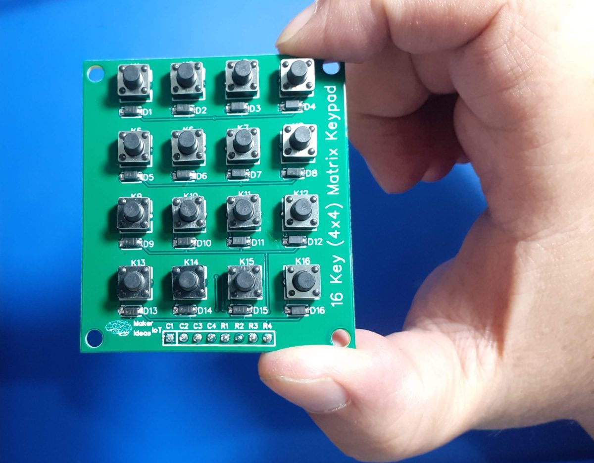
A matrix keypad is a type of keypad that uses a matrix of wires to connect the keys to the microcontroller. This allows for a smaller and more compact keypad than a traditional keypad, which uses a single row and column of wires for each key. Matrix keypads are also more reliable than conventional keypads, as they are less susceptible to damage from dirt and moisture.
How does a matrix keypad work?
A matrix keypad is made up of a number of rows and columns of keys. Each key is connected to two wires, one for the row and one for the column. When a key is pressed, it completes a circuit between the row and column wires. The microcontroller can then determine which key is pressed by checking which row and column wires are connected.
Why use a matrix keypad?
There are a number of reasons why you might want to use a matrix keypad in your project. Here are a few of the most common reasons:
Smaller size and footprint.
Reliability.
Cost savings.
What makes my design different from most others out there?
While the matrix keypad in its simplest form is constructed from only wires and switches, that simple approach can sometimes have some unwanted effects, especially when pressing multiple keys at the same time – a phenomenon called ghosting – where you get phantom keypresses. This is easily eliminated by adding a diode in series with each switch, usually on the row connection.
That single component fixes ghosting reliably but does not come without its own problems, the most important of these being that a keypad with diodes becomes “polarised” – current can only flow in a single direction through a switch. This can cause problems with some third-party libraries, as the designer of the keypad and the designer of the library very often has quite different ideas of what a row and a column mean in a keypad.
This is important, – here we go down the rabbit hole; in my understanding of the keypad scanning routine, a column runs from top to bottom, and a row from left to right. Keeping this in mind, the microcontroller will alternatively set each column HIGH, and configure each row as an input. When a key is pressed, current will flow from the specific column GPIO, through the switch, and into the Row GPIO, sending the input pin HIGH…
It is also possible to configure the columns as inputs, with internal pullups enabled, and have each Row pin as an output, configured to sink ( pull current to ground). This will cause the specific column to go low – thus identifying the pressed key…
These different ways of handling the problem of reading a key, and believe me, there are actually more variations, create a few unique problems. We may have to swap rows and columns as far as pin connections and firmware are concerned, as well as define a custom “keymap” to assign values to each key.
The Schematic
As we can see above, the schematic is very basic. 16 switches, 16 diodes and a single 8-way header pin. Pin 1 to 4 on the header is connected to Columns 1 to 4, and Pin 5 to 8 is connected to Rows 1 to 4.
The diodes prevent “ghosting currents from flowing into other keys in a row when multiple keys are pressed together. They also seem to help with other stray signals and interference.
The PCB
The PCB is a simple double-layer board. All components are mounted on the top layer.
To limit interference from stray signals, I have routed rows and columns on opposite sides of the PCB where possible.
Manufacturing
I choose PCBWay for my PCB manufacturing. This month, PCBWay is also celebrating its 9th anniversary, and that means that there are quite a lot of very special offers available.
Why? What makes them different from the rest? PCBWay‘s business goal is to be the most professional PCB manufacturer for prototyping and low-volume production work in the world. With more than a decade in the business, they are committed to meeting the needs of their customers from different industries in terms of quality, delivery, cost-effectiveness and any other demanding requests. As one of the most experienced PCB manufacturers and SMT Assemblers in China, they pride themselves to be our (the Makers) best business partners, as well as good friends in every aspect of our PCB manufacturing needs. They strive to make our R&D work easy and hassle-free.
How do they do that?
PCBWay is NOT a broker. That means that they do all manufacturing and assembly themselves, cutting out all the middlemen, and saving us money.
PCBWay’s online quoting system gives a very detailed and accurate picture of all costs upfront, including components and assembly costs. This saves a lot of time and hassle.
PCBWay gives you one-on-one customer support, that answers you in 5 minutes ( from the Website chat ), or by email within a few hours ( from your personal account manager). Issues are really resolved very quickly, not that there are many anyway, but, as we are all human, it is nice to know that when a gremlin rears its head, you have someone to talk to that will do his/her best to resolve your issue as soon as possible.
This project does not require a lot of specialised equipment to assemble. The SMD diodes can easily be soldered by hand, the same with the switches and 8-way header. In my case, I chose to solder the header pins on the back of the PCB, that way, I can later use the keypad in a suitable enclosure without having wires in the way.
Testing and Coding
Testing a matric keypad can sometimes be a challenge. In my case, a multimeter with clip leads, set to diode mode, with the leads connected to each column and row in turn, while minding the polarity, and pressing each key in that row in turn, verified continuity.
With that done, it was time to put my trusted Cytron Maker Uno to work, as this Arduino Clone has the added benefit of having LEDs on each of the GPIO lines, thus making it very easy to see what is happening.
I made use of a Keypad library in the Arduino IDE, mainly to cut down on the amount of coding, but also because it is easier to use a working piece of code, and then adapt that to my keypad.
Detailed Code examples for ESPHome are available on Patreon
/* @file CustomKeypad.pde || @version 1.0 || @author Alexander Brevig || @contact alexanderbrevig@gmail.com || || @description || | Demonstrates changing the keypad size and key values. || #
Edited by MakerIoT2020, with minor changes to make it function correctly with my custom keypad. I have also added a simple LED blinking routine to show that the Arduino is “alive” and that the Keypad code seems to be NON-blocking – which is quite important to me.
*/ #include <Keypad.h>
const byte ROWS = 4; //four rows const byte COLS = 4; //four columns //define the symbols on the buttons of the keypads char hexaKeys[ROWS][COLS] = { {‘1′,’4′,’7′,’*’}, {‘2′,’5′,’8′,’0’}, {‘3′,’6′,’9′,’#’}, {‘A’,’B’,’C’,’D’} }; byte rowPins[ROWS] = {2,3,4,5}; //connect to the row pinouts of the keypad byte colPins[COLS] = {6,7,8,9}; //connect to the column pinouts of the keypad /* * Due to libraries being written by different people, and our definitions about * what a row and a column are, is different, note that the rows in the code * is actually the columns on my PCB. This becomes true, due to the fact that my * PCB has Diodes on each switch, and that thus makes current flow in only one * direction/// * * it also has the “side effect” that keys are layout in a strange “mirrored” and * rotated way in the firmware. * it does however NOT affect the correct operation of the Keypad Module at all * */
const int LEDPin = LED_BUILTIN; int ledState = LOW; unsigned long prevmillis = 0; const long interval = 1000;
//initialize an instance of class NewKeypad Keypad customKeypad = Keypad( makeKeymap(hexaKeys), rowPins, colPins, ROWS, COLS);
This code works very well and allowed me to verify the correct operation of the keypad.
In conclusion
Making my own Keypad Module is a project that is long overdue. I have purchased a few online over the years, and as they were mostly of the membrane type, they did not last very long – it must be something to do with the ultra-cheap flexible PCB ribbon connector, since a quality membrane keypad can be quite expensive, and usually lasts quite a long time.
Having my own module available to experiment with will allow me to do some long-delayed improvements to many of my IoT modules. That code, mostly YAML for ESPHome, will be made available on Patreon.
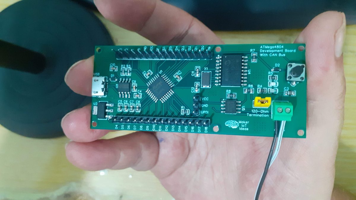
In This, Part 2 of my CAN Module series( Read Part 1 here), I will look at my recent modification of a previous ATMEGA4808 Development PCB to include CAN bus hardware. The ATMEGA4804 with CAN Bus development board is part of a set of “benchtop development tools” that I designed specifically to design some CAN Bus controlled Gadgets for use in my car…
The PCB is based on a previous project, in which we experimented with alternative chips to replace the ATMEGA328P.
MakerIoT2020 ATMEGA4808 Dev Board
As I was quite happy with the performance of this particular project, I thus decided to use it as the base for the CAN Bus module as well. The Added CAN Hardware adds only a few cm. to the board, keeping it quite compact, although, it will need a complete redesign once I finally get my gadgets finalised 🙂
What is on the PCB ?
The ATMEGA4808 and its supporting components dominate the left side of the PCB, with a USB connector and a CH340N providing the possibility to upload code to the chip using the Optiboot bootloader. I would however caution you, as there seem to be quite a lot of counterfeit CH340N chips floating around, I received two bad batches already, and from reliable suppliers as well… seems there is something fishy going on in the factory?? Answers anyone?
The Right side of the PCB is dedicated to the CAN Hardware, with the MCP2515 and TJA1050 taking centerstage here. While quite old, the MCP2515 is still readily available for the time being and is also quite affordable. Since I had a few left over from previous projects, I decided to once again make use of what I had on hand.
A 120-Ohm termination resistor ( selectable with a jumper), as well as a screw terminal connector, is provided. The board Reset button, as well as a power and user LED ( on D7), is also in that area of the PCB.
All GPIOs on the ATMEGA4808 were broken out onto header pins, to allow for maximum flexibility and access to features and peripherals on the chip.
Schematic and PCB Design
The Schematic, as mentioned before, is based entirely on a previous project of mine, with the CAN Hardware added onto that. ( I remind everyone once again, that this is a “tool” that I designed for myself to help in getting a specific job done. that will mean that it may or may not be very advanced, or suited for other peoples purposes… but , as a general bench module for CAN Bus development based on the ATMEGA4808, it will be perfect – that is what it was designed to do after all )
Schematic, ATMEGA4808 and supporting componentsSchematic, CAN Bus Hardware, MCP2515 and TJA1050
The PCB is a double layer approximately 8.1cm x 3.3cm rectangular module. 6 3.2mm mounting holes are provided.
Manufacturing
I choose PCBWay for my PCB manufacturing. Why? What makes them different from the rest?
PCBWay‘s business goal is to be the most professional PCB manufacturer for prototyping and low-volume production work in the world. With more than a decade in the business, they are committed to meeting the needs of their customers from different industries in terms of quality, delivery, cost-effectiveness and any other demanding requests. As one of the most experienced PCB manufacturers and SMT Assemblers in China, they pride themselves to be our (the Makers) best business partners, as well as good friends in every aspect of our PCB manufacturing needs. They strive to make our R&D work easy and hassle-free.
How do they do that?
PCBWay is NOT a broker. That means that they do all manufacturing and assembly themselves, cutting out all the middlemen, and saving us money.
PCBWay’s online quoting system gives a very detailed and accurate picture of all costs upfront, including components and assembly costs. This saves a lot of time and hassle.
PCBWay gives you one-on-one customer support, that answers you in 5 minutes ( from the Website chat ), or by email within a few hours ( from your personal account manager). Issues are really resolved very quickly, not that there are many anyway, but, as we are all human, it is nice to know that when a gremlin rears its head, you have someone to talk to that will do his/her best to resolve your issue as soon as possible.
To save myself time, and ensure that the project is assembled to a high quality standard, I once again opted to have a stencil manufactured in addition to the PCB alone. This is however not strictly required with this board, as the components can still be hand soldered, or solder paste can be manually applied using the method of your choice.
High-quality Stainless Stencil
I used my standard hotplate reflow soldering technique on this board, and it turned out very well indeed, with no solder bridges, making any reworking completely unnecessary, which can in no small part be directly attributed to the super accurate stencil that I used for solder paste application…
Assembled PCB
Testing
After assembly, I went through my standard testing ritual, while of course remembering that the ATMEGA4808 is a UPDI programmable chip, which means that you can not just use a USB cable on a brand-new chip…
I uploaded the Optiboot bootloader via that UPDI header, using my own UPDI programmer, that was also a previous project, one that I am very happy to have these days 🙂
A standard blink sketch followed, and then it was time to test the CAN hardware. For this I used Gary J Fowler’s MCP Can Libray ( the same one that I used with the ATTiny1616 a few days ago ), as well as the ATTiny1616 CAN Module that I build a few days ago…
As for the firmware, at this stage, as I am only concerned about testing actual CAN functionality, I made use of the CAN Loopback on both units, and then THe CAN Sender on the ATTiny1616 and the CAN Receiver on the 4808… These sketches are all available in the library examples… so find them there.
Pinouts for the connections to the MCP2515 from the ATMEGA4808 is as follows:
CS is on Pin D7, MISO on D5, MOSI on D4, SCK on D6 and the Interrupt on D10
The ATTiny1616, which I did not mention in part one, is as follows: CS on D13,MISO on D15, MOSI on D14, SCK on D16 and the Interrupt on D12
Conclusion
Testing went well, with everything working as expected, with the exception of another batch of CH340N chips being suspect… This does however not really bother me, as I am quite comfortable with using UPDI to upload code, as well as using an external USB-to-serial adapter, connected directly to the UART on the ATMEGA4808.
Cosmetically, I made a labelling error on the silkscreen of the CAN Bus connector, swapping Can H and CAN L… once again, this is not a problem to me.
My thanks to PCBWay for another extremely well-made PCB.
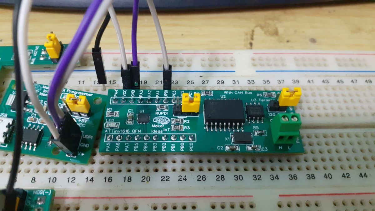
ATTiny1616 QFN with Can bus support on a breadboard
A short while ago, I started looking at alternatives to the ATMEGA328P ( the chip used in the standard Arduino Uno). That experiment turned out quite well, with two of the three chips turning out to be useful, the ATTiny1616 and the Atmega 4808 – The ATTiny 202, while working great, has quite a few severe limitations, due to the size of its memory, as well as library support, limiting its actual useful use quite a bit for my purposes.
In this post, which is part of a two-part series, I will look at adding dedicated CAN Bus support to the 1616 and 8408. I am planning to add some gadgets to my car, and would like to have it controlled by a CAN bus interface, and just maybe, interfacing with the CAN bus on the car as well – at least in the future…
This experiment will thus consist of two prototypes with onboard CAN hardware, to be initially used on the bench while building and testing my gadgets – more on them later, if and when they work out the way that I imagine.
What is on the PCB
The ATTiny1616 microcontroller, in a QFN package, has been married to a MCP2515 and a TJA1050. These chips, while old, are still easy to get hold of, and I have quite a few of them lying around from previous projects. It did thus seem to be a good starting point. The fact that their libraries also works perfectly with the ATTiny1616 and Atmega4808 also went a long way towards selecting them for the project.
The PCB is similar to the ATTiny1616 QFN breakout that I have designed before but with the addition of the CAN-related components.
ATTiny1616 QFN development board with CAN bus, after reflow soldering
Schematic and PCB Design
The schematic is a variation on the earlier breakout PBC, with the addition of the CAN-related components.
The PCB design has also not changed a lot, I have just added the CAN components to the right hand side of the PCB, and adjusted the routing.
3D render of the PCB, with the header pins in non-breadboard configuration – with the CAN bus connector not fitted.
Manufacturing
I choose PCBWay for my PCB manufacturing. Why? What makes them different from the rest?
PCBWay‘s business goal is to be the most professional PCB manufacturer for prototyping and low-volume production work in the world. With more than a decade in the business, they are committed to meeting the needs of their customers from different industries in terms of quality, delivery, cost-effectiveness and any other demanding requests. As one of the most experienced PCB manufacturers and SMT Assemblers in China, they pride themselves to be our (the Makers) best business partners, as well as good friends in every aspect of our PCB manufacturing needs. They strive to make our R&D work easy and hassle-free.
How do they do that?
PCBWay is NOT a broker. That means that they do all manufacturing and assembly themselves, cutting out all the middlemen, and saving us money.
PCBWay’s online quoting system gives a very detailed and accurate picture of all costs upfront, including components and assembly costs. This saves a lot of time and hassle.
PCBWay gives you one-on-one customer support, that answers you in 5 minutes ( from the Website chat ), or by email within a few hours ( from your personal account manager). Issues are really resolved very quickly, not that there are many anyway, but, as we are all human, it is nice to know that when a gremlin rears its head, you have someone to talk to that will do his/her best to resolve your issue as soon as possible.
I usually can not wait to receive my creations back from the factory – I mean, how can somebody not get excited about receiving their own PCBs back from the factory, especially if you know they will be of the high quality that I have come to trust with all of my PCBWay orders?
This is especially true of the smaller PCBs, as well as those with smaller-sized QFN components, with this board definitely not being an exception.
PCBs in factory packagingPCBs in protective wrapping, just after opening the package
Closeup view of the top side of the PCB
This PCB once again requires the use of a stencil, to accurately apply just the right amount of solder paste to the pads, especially the small QFN package pads of the ATTiny 1616…
High-quality stainless steel, laser cut stencil.
Stencils, at least from my point of view, can be a controversial subject, with some hobbyists arguing that they are not worth the additional expense… I do however believe that they actually save you a lot, in time that you don’t waste on reworking a PCB due to solder bridges, in the correct amount of solder paste that is applied, in the correct thickness, and also time not wasted on the cleanup of the mess that can result from manually applying solder paste.
PCB ready for reflow soldering, after manually placing the components in their respective places
The PCB is now reflow soldered with a hot plate, and allowed to slowly cool down afterwards, to reduce thermal shock damage to the joints, that may result from a too-quick cooldown cycle. While I do not own a dedicated reflow oven, the hotplate that I use, seems to match the reflow profile ramp-up of my solder paste, and most of the components perfectly. After achieving a complete solder melt, at about 223 degrees C, I usually switch of the hot plate, and carefully move the PCB towards the edge of the unit, that area is usually a bit cooler than the centre. leaving it there for about 5 to 8 minutes, allow the solder to slowly solidify, after which I remove it and place it on a silicone mat to cool completely.
Through-hole component soldering, and testing
The next step is soldering all the through-hole components, usually header pins and connectors into their respective places. The board is then placed onto a solderless breadboard, and various test sketches are uploaded via a homemade UPDI programmer.
These include the infamous blink sketch, to make sure the chip is alive and survived the reflow soldering. That is followed by a CAN loopback test, and then the actual CAN firmware… I make use of the excellent MCP Can library from Garry J Fowler, as well as the megaTinyCore Arduino core, from Spence Konde.
My thanks to both of these gentlemen, for their excellent and easy-to-use software. A special shoutout to Garry J Fowler, since his MCP Can library correctly releases the CE pin of the device when not in use, thus not locking up the spi bus. [ This is something that many other libraries do not bother to care about ] …
Conclusion
This was once again a fun project to design and assemble. The real testing and development can now start at full speed, as this is just meant to be a tool, with a further revision later down the line. It does of course help a whole lot that I can completely trust my PCB manufacturer, PCBWay, to deliver my PCBs to me EXACTLY as I designed them, and at extremely high quality and precision! Thank you for that!
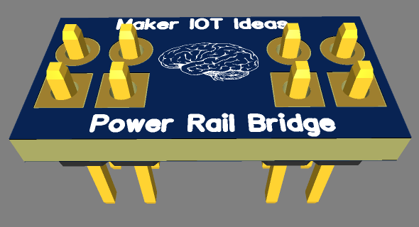
This is a sort of tongue-in-the-cheek project, that started with good intentions, and ended up wholly over-engineered and sort of “broken” due to adding “added features” like LEDs and an additional power header.
What was the initial intention?
[This is what I actually wanted to achieve]
My breadboards all have interrupted power rails, and it is thus always necessary to bridge them with jumper wires to have a continuous rail. This is needed because I very often have more than one project on a single breadboard, and do not want to have to use separate power modules for each. I also tend to test out some part of a circuit on a separate part of the breadboard, before incorporating it into the main circuit.
[ I completely overdesigned this, ending up with something completely different from what I wanted]
Wire jumpers are definitely the easier and fastest, but having been struck by a “what if I do this instead” moment, this tiny PCB was designed and subsequently sent to manufacturing…
So does it work?
Yes, it works, for its intended purpose of bridging the power rails, but that is where the wheels come off. Let me explain, trust me, it will be fun, and we can all laugh at it in the end…
Breadboard power rails are usually marked Red for positive, and Blue or Black for negative… Most people on this planet are also right-handed, and would thus place a power module on the right-hand side of a breadboard ( although some won’t..) Being left-handed myself, and still trying to please right-handed people, my power module will be “upside down” on the left-hand side of a breadboard… which is fine with me, as I remember to swap the colours of the rails in my mind, making red negative and blue positive… not a big issue is you always do it that way…
So what went wrong…
While designing this, I initially planned on a simple PCB bridge, with a jumper on the positive line, acting as a switch, and a continuous ground that is always connected.. all fine, problem number 1 being that I looked at the colours of the power rails while designing it, measuring the gaps etc to get the spacing just right…
Problem number 2 is that the top and bottom rails are in the same configuration, Red at the top, blue at the bottom… and thus plugging in a bridge into either should be ok… and it really should have been, if I did not decide to add a status LED on each side of the bridge, and an additional power header… because turns out that I forgot that the bridge at the top will in effect be “mirrored” when plugged in ( and thus having components that are reversed polarity) – mirrored, due to the fact that you now have to plug the top rail bridge upside down into the breadboard, because it will otherwise interfere with the prototyping space
[This was the direct effect of my lack of attention to detail – and yes, it works perfectly in this configuration – if we ignore the wasted space on the top half of the board]
[This is the practical reality – one bridge must be installed ‘upside-down’]
Lesson learned; I can be quite scatterbrained at times, especially when juggling a few projects and customers at the same time ( I am only human anyway ). Thus this project, although it looks nice, and can be useful, needs to go back to the drawing board for a complete redesign, without all those “added features”
The Schematic
The schematic is straightforward, with no surprises. Two LEDs ( polarity sensitive ) and then those headers and jumpers, which also need up being polarity sensitive – in a manner of speaking
Quite different from what I originally wanted to do
Manufacturing
I choose PCBWay for my PCB manufacturing. Why? What makes them different from the rest?
PCBWay‘s business goal is to be the most professional PCB manufacturer for prototyping and low-volume production work in the world. With more than a decade in the business, they are committed to meeting the needs of their customers from different industries in terms of quality, delivery, cost-effectiveness and any other demanding requests. As one of the most experienced PCB manufacturers and SMT Assemblers in China, they pride themselves to be our (the Makers) best business partners, as well as good friends in every aspect of our PCB manufacturing needs. They strive to make our R&D work easy and hassle-free.
How do they do that?
PCBWay is NOT a broker. That means that they do all manufacturing and assembly themselves, cutting out all the middlemen, and saving us money.
PCBWay’s online quoting system gives a very detailed and accurate picture of all costs upfront, including components and assembly costs. This saves a lot of time and hassle.
PCBWay gives you one-on-one customer support, that answers you in 5 minutes ( from the Website chat ), or by email within a few hours ( from your personal account manager). Issues are really resolved very quickly, not that there are many anyway, but, as we are all human, it is nice to know that when a gremlin rears its head, you have someone to talk to that will do his/her best to resolve your issue as soon as possible.
This project served many purposes beyond the actual use of the PCB that was designed. In a way, I am quite happy that I screwed up so badly on this one – here is the reason why:
Because I do quite a lot of PCB design each month, for customers or personal projects, I often tend to get a bit over-confident, and also rush things through, while believing that I will catch every mistake before I send something off to production. Normally, I am quite good at that, and my error rate is actually quite low… But, This month, being quite busier than usual, and having had a fair amount of distractions, served as the perfect lesson to drag me down a notch or two, and remind me that I have to be way more attentive, especially when things are going hectic, and there are a few projects to juggle around at the same time.
The second reason why it is a good thing when the wheels come off like this, once in a while, is that it serves as a perfect example of what your PCB manufacturer’s actual job is. So, this is especially for the new guys that may not know this: Your PCB Manufacturer has only one job – To manufacture your PCB EXACTLY AS YOU DESIGNED IT – Scary, right? Sure, they will let you know if your design falls outside of their tolerances of capabilities. They will let you know if your board fails a flying probe test if you have that kind of arrangement with them… But it is NEVER their job to correct or attempt to change any of your design files.
So, what is the moral of the story, regarding both of the points that I made above?
If you screw up on the design, it is your, and only your fault. Nobody else is to blame, ever. The buck stops with you, the designer.