The Assembly of the ATTiny1616 Can Bus Controller PCB will be covered in this post. This PCB took quite a bit of time, due to having a real-world job that takes up an extreme amount of my time.
Enough of that, let’s get started
The PCB
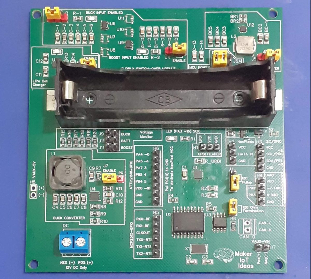
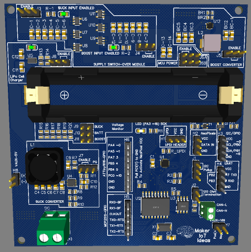
The PCB is a double layer, with mostly SMD components, and as mentioned in the initial post, broken up into functional blocks to make testing easier. I will also take the time to mention some performance and problem issues that I have encountered during the testing phase here are well
These include: – a buck converter power supply module to provide 5v DC. – a single-cell lipo cell charger circuit – an ideal diode supply or-ing circuit – a boost converter – various jumpers, so enable/disable certain parts of the circuit – microcontroller and logic circuits
The bare PCB
All of the circuit modules mentioned have been covered in detail in previous posts, so I will only briefly review some of them here to highlight some changes I have made to the original circuits.
The ideal diode supply or-ing circuit has been modified to use 3 ideal diode chips in parallel per “channel”. This is “experimental” from my point of view since I am unsure if it would actually perform as expected. I had to do this due to experiencing great difficulty in obtaining a suitable high-current component at a reasonable cost and in a suitable footprint.
This question remains unanswered, as I encountered a double whammy with no stock issue forcing me to use one device per channel. I shall update the performance of this experiment soon when I receive the back-ordered components.
The performance of the boost converter can at best be described as temperamental. This is definitively an assembly issue on my side, as the controller chip is tiny (approx. 2mm x 2mm with 14 leads), and hand assembly of this with a stencil and hot-plate reflow almost always results in the need to hot-air rework and then possibly damaging the chip with heat or other issues.
I am currently investigating an alternative chip to use in future versions of the PCB to remove this issue. When the circuit works, it is rock solid and gives great performance. Maybe someone from Microchip (#not sponsored) can give some advice here…
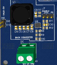
The Buck converter performs solidly as usual, great little device! No complaints there as usual.
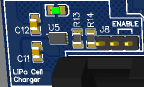
The Lipo-cell charger performs as expected, with no issues to report.
As seen in the picture above, I have placed yellow jumpers to make it easy to enable/disable parts of the circuit to aid in testing and debugging. These help quite a lot.
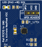
The ATTiny 1616 is solid, as can be expected, and functions exactly as expected. Some users would have to replace the R_UPDI resistor with a 0ohm link, depending on which UPDI programmer you use. Since I use my own custom-made UPDI Programmer as recommended in a circuit by Spence Konde/Dr Izzy on his excellent megatinyCore documentation site, I have no issues with UPDI.
The Can-Bus hardware functions as expected, with no issues to report.
There is also an error on the silkscreen, Pin_PC1 should be pulled HIGH to activate the VCC line for the neoPixel strip, NOT LOW as printed on the silkscreen.
Manufacturing the PCB
I choose PCBWay for my PCB manufacturing. Why? What makes them different from the rest?
PCBWay‘s business goal is to be the most professional PCB manufacturer for prototyping and low-volume production work in the world. With more than a decade in the business, they are committed to meeting the needs of their customers from different industries in terms of quality, delivery, cost-effectiveness and any other demanding requests. As one of the most experienced PCB manufacturers and SMT Assemblers in China, they pride themselves to be our (the Makers) best business partners, as well as good friends in every aspect of our PCB manufacturing needs. They strive to make our R&D work easy and hassle-free.
How do they do that?
PCBWay is NOT a broker. That means that they do all manufacturing and assembly themselves, cutting out all the middlemen, and saving us money.
PCBWay’s online quoting system gives a very detailed and accurate picture of all costs upfront, including components and assembly costs. This saves a lot of time and hassle.
PCBWay gives you one-on-one customer support, that answers you in 5 minutes ( from the Website chat ), or by email within a few hours ( from your personal account manager). Issues are really resolved very quickly, not that there are many anyway, but, as we are all human, it is nice to know that when a gremlin rears its head, you have someone to talk to who will do his/her best to resolve your issue as soon as possible.
Due to the size of some of the components on this PCB, a stencil is compulsory for hand assembly of this PCB, or even better, have it professionally assembled by your PCB manufacturer. It will save you a lot of headaches during assembly
The stencil that I got from PCBWAy made things so much easierThe assembled PCB, without CAN connector and Lipo Cell
Conclusion
This project took way longer than initially planned, due to many issues including logistics, component availability, the need to rework some areas of the board, and being super busy at my day-job. The firmware is still a work in progress, with bits and pieces of code floating around, hacked together to test basic functionality but nothing else.
I hope to complete this project very shortly, and after a final revision of the hardware, to get rid of some issues that bug me, to have a very useable piece of equipment to finally install in my car as planned from the very beginning
Over the last few months, we have been working on several prototypes, and some of our regular visitors may recognise some parts of this PCB. But let us begin by telling you what this is about.
As many of you may know, we have already designed several Can-Bus-related development boards, including one based on the ATTiny1616… So why the repeat then? Well, in some of my previous projects, I hinted at combining a buck converter, boost converter, lipo cell charger and Ideal Diode circuit into one PCB. I did at that time not tell you why.
To make a long story short, this project will eventually be used in my car, to provide more modern cabin lighting, which is quite a bit more than the standard on-or-off and on-when-open-the-door, off-when-close-the-door type of thing…
I own an old Honda City that I use mainly for a run-around to and from the farm, as well as seeing clients… Roads are bad, and this older car (actually quite old – 22 years) is the most cost-effective, in terms of being able to repair by myself, and not be worried about it if it gets a bit abused.
Unfortunately, the technology in the car is dated… a single yellowish cabin light right in the centre of the cabin – and not bright at all. Having to use the car at night, and then frequently scratching around in equipment bags when arriving at a client, becomes a pain with bad light… So I have decided to give it a bit of an upgrade and add CAN-bus-controlled NEO-Pixels to the cabin. For now, let’s say three sets, left, right and centre of the cabin. I also prefer a red light at night over white, especially if I have to drive again soon afterwards – a simple remnant from my days in the military, where it became quite clear how white light can temporarily damage your night vision.
NeoPixels can also be dimmed/brightened and seem relatively inexpensive.
Let us take a closer look at exactly what I want to do…
Powering the module
For the sake of clarity, this particular module will be installed front and centre in the cabin, just behind the rearview mirror. It will control two sets of 8 neopixels ( or up to 12 per module ) on two separate PCBs, which will cover the driver and front passenger area of the cabin.
The module will be powered by the vehicle’s 12v battery, as well as from a single 18650 Lipo cell. This means that we would need some clever tricks, in the form of a buck converter to step down the 12v to 5v, a way to monitor and recharge the lipo cell, a boost converter to boost the lipo cell voltage back up to 5v as well as a voltage “OR-ing circuit” to prevent reverse charging the lipo cell etc…
In its current state, the PCB is to be considered a test rig, since I have quite a few unknown variables that need to be thoroughly tested before actually installing this thing into a vehicle.
These are : 1) I would like to know if the ideal diode chip that I used functions well when used in a parallel setup, The reason for that is, that a single chip is capable of just about 1A of current… thus, in my reasoning, placing 3 in parallel would give me the 3A capability that I require – Let’s see if it does… I could also not get hold of a suitable 3A capable ideal diode chip that was cost-effective, or did not have some strange MOQ or other logistics issues ( Yeah, seems like getting some stuff in SE Asia is difficult unless you are willing to pay unnecessary “special” charges and import duties etc … Element14 ( not sponsored) seems to have a limited selection of ideal diode solutions, but their pricing is good, and there are minimum hassles with shipping etc… I don’t bother with the other two big suppliers, D…. and M…. as they have too much red tape for a hobbyist to navigate to make it cost-effective to shop from them.))
2) Providing that the ideal diode solution does work as expected ( on the PCB) – having tested it on a breadboard seems to be working fine, there is the issue of monitoring the lipo cell, getting it charged, controlling the boost converter to provide power when needed etc…
All of this means that all the separate circuit modules on the PCB can be enabled or disabled by jumpers, and later, if all works as expected, maybe by another controller PCB… Who knows?
Getting back to power the PCB, I have used my standard buck converter circuit, based around the MP9943. This circuit seems to be very reliable, provides enough current, and is cost-effective.
I have also provided an auxiliary voltage output ( 5v) and some telemetry and control capability to the buck converter circuit, in the form of an enable-disable jumper, and the PG signal from the chip, to maybe be interfaced with a microcontroller later.
Charging the Lipo Cell
Once again, I made use of an existing circuit, with which I have had a lot of success in the past. This circuit, based on the MCP73832 from Microchip ( not sponsored) served me quite well in previous projects, and is once again, cost-effective and easy to implement. One negative is that they do seem to be a bit finicky, and not extremely robust – but when they work, they excel at it…
Once again, I decided to provide control logic to enable or disable this part of the circuit completely if needed.
Supply “OR-ing” circuit
This is the most experimental part of this entire circuit board, since, as mentioned above, the MAX40200 is rated at 1A maximum current. It is tiny and cheap, and also readily available… I am hoping that by using them in parallel I can achieve my goal of allowing the full 3A of current to flow from the buck converter, without releasing any “magic smoke” or other issues…
While, at the time of writing, I have not yet received the PCB, I am positive that all may just be fine, it remains to be seen how this will turn out during actual testing of the board.
Note that I have used a total of 6 of these, U8 to U11, with 3 per “voltage/current supply” channel. J3 and J4 are used to enable or disable the two supplies, with J3 being the buck converter input, in turn, powered from the vehicle 12v supply, and J4 begin the output from the boost converter, powered by the Lipo cell.
Boost converter circuit and MCU power
The boost converter is based on the MP3423, also from Microchip ( not sponsored). This circuit also performed very well in my initial test projects, with the only issue being it extremely tiny footprint, which really makes it quite difficult to use in a hobby environment, even with hot air and reflow equipment available… It is however also quite cheap, and readily available…
J5 provides enable-disable control to this part of the circuit.
With this relatively complicated power supply circuit, I thought it necessary to be able to completely isolate the ATTiny1616 and other integrated circuits from any power until I am completely sure everything works as planned…
J6A and J6B thus form a complete electrical isolation “breaker” that will prevent any voltage being provided to the microcontroller and other components on the PCB. I have doubled up on these jumpers, to allow for sufficient current flow, since I plan to use quite a few NeoPixels on this PCB… With up to 60mA of current required per pixel, that quickly adds up…
Voltage monitoring
Provision was made to monitor the output voltages of the Lipo Cell, and buck and boost converters by using the analog inputs on the ATTiny1616. These can be selected by setting the jumpers on J9, J10 and J11
Alternatively, the analog inputs can be used for other applications be leaving the jumpers off, in which case these GPIO’s will be available on H6 as PA4, PA5 and PA7
The ATTiny1616 microcontroller and UPDI programming port
The heart of this PCB is the ATTiny1616 microcontroller, (microchip, not sponsored)
I decided to use the chip once again due to its low cost, as well as the fact that I do not need a very powerful processor for this application. The only issue is that requires UPDI programming. In my case, I have had no issue with that yet, but other readers did mention that they had issues with them…
The UPDI header is at H1. This header can also be used to power the processor and other integrated circuits on the PCB independently from the Power supply, like in the case where J6A and J6B are left unconnected. This use case will provide me with more testing opportunities to test the board without possible variables from the power supply circuit(s).
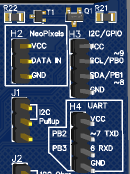
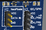
Peripherals like I2C and the UART were broken out onto headers H3 for I2C, H4 for UART. These can also be used as GPIO pins ( remember to disable the I2C pullup in J1)
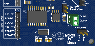
CAN-Bus Support
CAN-Bus support is provided by the MCP2515 (U2) and TJA1050 (U3) chips.
With access to the MCP2515 GPIO pins on H5. J2 is a 120ohm termination resistor, usually enabled at the start and end of the bus to prevent reflections.
CAN-0 is connected to the bus. An additional 12v input/output header is provided at H7
NeoPixel Header H2
The NeoPixel strips are connected to H2. They are controlled from GPIO PA6 on the ATTiny1616. I have designed around a total of 24 of these at a maximum, with a total current requirement of 1.4A ( 24 x 60mA max per pixel / 1000 = 1.44 A) .
One important fact to know about NeoPixels is that the consume about 1mA per pixel even when in the OFF state. This is due to the internal control chip requiring power to operate. While 1mA bay be a very small amount of current, a lot of them does however quickly add up, and can thus potentially drain a battery completely over time…
To prevent this from happening, I have included a PMOS switch on the VCC pin at H2. This means that no power will be fed to the Neopixel strips unless you specifically pull GPIO PC1 low.
Manufacturing the PCB
I choose PCBWay for my PCB manufacturing. Why? What makes them different from the rest?
PCBWay‘s business goal is to be the most professional PCB manufacturer for prototyping and low-volume production work in the world. With more than a decade in the business, they are committed to meeting the needs of their customers from different industries in terms of quality, delivery, cost-effectiveness and any other demanding requests. As one of the most experienced PCB manufacturers and SMT Assemblers in China, they pride themselves to be our (the Makers) best business partners, as well as good friends in every aspect of our PCB manufacturing needs. They strive to make our R&D work easy and hassle-free.
How do they do that?
PCBWay is NOT a broker. That means that they do all manufacturing and assembly themselves, cutting out all the middlemen, and saving us money.
PCBWay’s online quoting system gives a very detailed and accurate picture of all costs upfront, including components and assembly costs. This saves a lot of time and hassle.
PCBWay gives you one-on-one customer support, that answers you in 5 minutes ( from the Website chat ), or by email within a few hours ( from your personal account manager). Issues are really resolved very quickly, not that there are many anyway, but, as we are all human, it is nice to know that when a gremlin rears its head, you have someone to talk to who will do his/her best to resolve your issue as soon as possible.
This project has a lot of specific details regarding testing and assembly. Therefore I have decided to put all of that in a separate post, that you can access here.
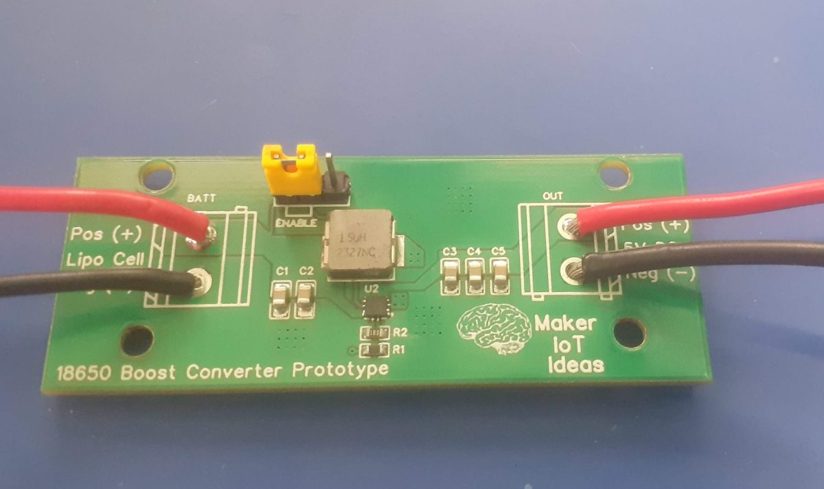
As part of an ongoing project, this tiny boost converter was designed to be used to power some of my projects, as well as become a part of a much-needed add-on circuit to the single-cell 18650 charger PCB that I designed a while ago.
I received a lot of very useful comments from readers about the circuit below ( the single-cell 18560 Lipo charger). Most of these comments were related to adding a boost converter to the circuit, to add a little more versatility to the circuit.
I never just add something though, and as such, this boost converter prototype was designed to test out the components and design before incorporating it into the main design. That way, I can iron out any problems before adding it to a bigger circuit.
The boost converter is based on the MP3423GG-Z, from MPS. I have decided to stay very close to their recommended application notes, so the circuit is stock standard. Another way to ensure that performance is what I want it to be, and also, to be frank, because I don’t believe I need to make any changes to the manufacturer-recommended circuit.
Some other comments suggested the use of “ideal diodes” at the output , in order to be able to daisy-chain the chargers. That will be addressed in a later post this month, as I am also currently testing out one of the many “ideal diode” integrated circuit chips available – in this case the MAX40200.
Being a “prototype” I did not bother with adding proper connectors to this version, as it will only be used for a short while. Soldering the supply and output wires directly to the PCB will thus be sufficient for the time being.
Design and Manufacturing
I choose PCBWay for my PCB manufacturing. Why? What makes them different from the rest?
PCBWay‘s business goal is to be the most professional PCB manufacturer for prototyping and low-volume production work in the world. With more than a decade in the business, they are committed to meeting the needs of their customers from different industries in terms of quality, delivery, cost-effectiveness and any other demanding requests. As one of the most experienced PCB manufacturers and SMT Assemblers in China, they pride themselves to be our (the Makers) best business partners, as well as good friends in every aspect of our PCB manufacturing needs. They strive to make our R&D work easy and hassle-free.
How do they do that?
PCBWay is NOT a broker. That means that they do all manufacturing and assembly themselves, cutting out all the middlemen, and saving us money.
PCBWay’s online quoting system gives a very detailed and accurate picture of all costs upfront, including components and assembly costs. This saves a lot of time and hassle.
PCBWay gives you one-on-one customer support, that answers you in 5 minutes ( from the Website chat ), or by email within a few hours ( from your personal account manager). Issues are really resolved very quickly, not that there are many anyway, but, as we are all human, it is nice to know that when a gremlin rears its head, you have someone to talk to who will do his/her best to resolve your issue as soon as possible.
This PCB really would benefit from having a stencil available when you assemble it by hand. The MP3423GG-Z is super tiny, so having a guide to apply just the right amount of solder paste to the pads will go a long long way to make sure that there is no reworking needed.
All of the other components are quite manageable, being only a couple of 0805 and 0603 resistors, and an inductor. I reflow soldered everything at the same time with a hotplate. It is worth noting that I did have to remove and replace the MP3423GG-Z once during the reflow process… tiny solder bridges formed between some pins, but carefully lifting it up with a pair of tweezers, and placing it onto the pads again got rid of those completely.
We may be tempted to “leave it off the board, wait for the solder to flow and then place the component onto the molten solder…” I am not too sure about the thermal stresses that that method may or may not induce in the component… so, I prefer having it heat up slowly with the rest of the components/ and then make a quick adjustment if needed… Comments on this anyone?
Testing and final thoughts
Testing the boost converter went without any problems. It delivers a stable 5.15v DC at the output, from an input voltage of 3.3v to 4.2v. I did not test it lower than that yet… Current output seems quite stable, and the voltage does not fluctuate under load ( I tested with 2 LED COB lights, each drawing 600mA, connected in series – thus 1.2A — That is definitely the maximum current that I intend to draw from this device, although it is rated at 3A
Ripple current seems to be within the 100mV stated in the datasheet.
In summary, I believe the device performs the intended duty that i set out to design. The assembly is a bit tricky due to the small size of the MP3423GG-Z, as well as my “not-so-good” eyesight. All that aside, I am ready to advance to the next phase of the overall project – revision 2 of the Single Cell 18650 Lipo Charger.
Imagine You are working on a project late on a Friday evening and suddenly your mouse stops working… You can not scroll, and the right-side button won’t respond to your clicks… At the same time, you have a project design that has got to get finished… and the shops are all closed already…
These were the circumstances that led to the birth of “The Emergency Mouse” – A project born out of necessity. How did I solve my problem?
Having access to a lot of electronic modules saved the day. As a maker, I always have various modules and gadgets lying around, and on this unfortunate evening, I remember that the RP2040 has USB HID support. Combine that with a simple Analog Joystick module, a rotary encoder and some push buttons, add about 30 minutes worth of browsing the internet, struggling along with a broken mouse – we have to give the old one credit, it had a very long and hard life, and I finally found some example code that did not just jiggle the mouse pointer or do something equally silly…
The only problem with all of that was that the code was for CircuitPython… I generally dislike using Python on a Microcontroller, as I believe it is better suited for the computer, but, I am warming up to the idea… slowly…
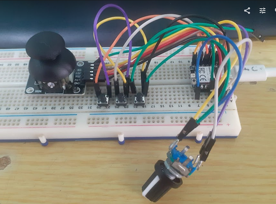
The initial fix – a mess of wires on a breadboard
I quickly grabbed a RaspBerry Pi Pico out of a box, plugged it into a breadboard, loaded Circuitpyth and fired up the example code I got on the internet… While promising, It did not exactly do what I wanted… so a few minutes later, after some coding, I had a moving pointer, controlled by the small thumb joystick module, and with the center button as a “right button”…
So far so good… I can work more easily, but still did not have scrolling… so lets hit the datasheets and documentation on the Adafruit Website (not sponsored) and add a rotary encoder… works well, add more buttons, etc etc…
Eventually it was all done, and about 1 hour has passed, but we were left with a huge ugly mess on a breadboard, and a lot of unused GPIO pins.. So this Pico must go… it can be used for something more useful later…
Then my eye fell on a SEEED Studio XIAO RP2040 module, almost begging to be used… This is smaller, more compact… lets try that …
Initial breadboard version, here shown with the SEEED Studio XIAO RP2040
What functions did this “mouse” have
After changing to the XIAO RP2040, things went very quick…
I added two buttons for scrolling up and down, simulating a mouse wheel, but kept the encoder… which, while VERY awkward to use at this stage, definitely had potential in the long run…
I also added another button to take over the function of a right button, while the center button on the joystick became left…
Disaster averted, with only about 2 hours wasted, I returned to my project and managed to get it finished using the “improvised-mouse-on-the-breadboard” contraption…
That night, while lying in bed, trying to get to fall asleep, the possibilities of this “contraption-on-the-breadboard” would not let me go… I am fairly old-school, and during the late 80’s and early 90’s owned quite a few “roller-ball” mouse devices… these later became trackballs, and being excessively overpriced, was promptly removed from my environment – the old ones did not last very long, and the new ones were, as I said, overly expensive…
I did however never forget the ease of use that first “rollerball mouse” gave me all that years ago, using only my thumb to move it around etc etc…
This idea would have to be investigated, and turned into a PCB… with that, I finally drifted off to sleep…
The PCB design
The next morning came, and due to reasons unknown, as well as being lazy, I decided not to leave the house, and go buy a new mouse. lets try online… No, they are crazy – I am not paying that for a mouse!
All the time using the “contraption-on-the-breadboard”. So this thing started growing on me… lets design a PCB
The Initial PCB design
After a few hours spent on deciding on optimal layout, I came up with this… It was still a bit unrefined, but definitely had potential… It lacked a dedicated center button, and those momentary push-buttons requires a lot of force to use… but as a prototype, why not…
Let’s get this manufactured.
For this build, since I used a SEEED Studio module, I decided to send it to SEEED for manufacturing… no need to get components from various places, as they should have all in stock…
Seeed Studio’s Fusion service seamlessly marries convenience with full-feature capabilities in one simple platform. Whether you are prototyping or looking for a mass production partner or based on open source product customization requirements and other design manufacturing services, Seeed Studio Fusion service is catered to your needs starting with a simple online platform. https://www.seeedstudio.com/fusion.html
The PCB arrives from the factory
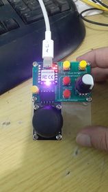
During the entire time that it took for the PCB to be manufactured and assembled, I was still using this “homemade mouse” – I started calling it a mouse now… and it was still on the breadboard… I never did bother to buy a new mouse, yet..
The PCB Arrived today, and apart from a few small soldering issues, looked great… I still had to do a bit of assembly on my own, as there was an issue with the components I wanted being out of stock.. I have plenty in stock of my own, so opted to do manual assembly…
The completed PCB now only needed a joystick, and some firmware…
After adding a few button caps, and mounting everything to a piece of acrylic plate, I had a working prototype…
The Firmware
As mentioned above, the device runs on CircuitPyton. As Such, there are quite a lot of “examples” on the internet, showing you how to do many USB HID “mouse” like things, but generally being completely useless…
I have thus spent quite a lot of time up to now, writing and refining my own version of the firmware, that is actually useful and does actually work.
It has the following features: X-Y axis control of the mouse pointer via a thumb joystick, with a left click function on the center joystick button, as well as a dedicated “left” button.
A dedicated “right” button A “virtual center” button made up of simultaneously pressing left and right
Up and down scrolling either using the rotary encoder as a “mouse wheel” or via dedicated up and down pushbuttons.
A dedicated Reset button – this is necessary, as I can not seem to get the device to initialise correctly at computer bootup.
Various software functions, like changing the pointer acceleration by pressing the center button on the rotary encoder
and most importantly, hiding the Circuitpyton drive, only showing it when I actually need access to the code in this device…
Various statuses are indicated using the NeoPixel on the XIAO, making it easy to see in what state the device is operating.
As such, I shall NOT be releasing the firmware at this moment, as it is still far from being perfect. It works, but it can be way better…
Summary and next steps
Since its “birth” late on a Friday night, about 3 weeks ago, I have been using this device, in its various forms as my primary pointer device. It is growing on me more every day, and it is quite comfortable to use – If we ignore the fact that it is not in a suitable enclosure and that I am still making small changes to the firmware from time to time.
I am already planning the next revision, in which I shall replace the momentary push-buttons with proper microswitches, as well as try my hand at designing a proper enclosure.
If you are a 3D printing expert and want to collaborate with me on this, let’s talk…
COB LED lights, or Chip-on-Board LED lights, are a type of LED light that has all of the LED chips mounted on a single substrate. This makes them more efficient than traditional LED lights, which have individual LED chips mounted on a circuit board. COB LED lights also produce a more uniform light output, and they can be used in a wider variety of applications.
Here are some of the benefits of using LED COB lights:
are very efficient, and they can produce up to 100 lumens per watt. This means that they use less energy than traditional light bulbs, and they can save you money on your energy bills.
produce a more uniform light output than traditional LED lights. This means that they do not create hot spots or shadows, and they provide a more comfortable light to work under.
are very durable, and they can last for many years. They are not as susceptible to damage from heat or vibration as traditional light bulbs, and they can withstand harsh conditions.
can be used in a wide variety of applications, including indoor and outdoor lighting, commercial and residential lighting, and automotive lighting.
They can however be quite a pain to power in a traditional 110v/220v AC wired house or workshop, as some of them actually required DC current to work. I have decided to use a pair of them to provide additional, dimmable light at my electronics workbench, a place where extra light is sometimes a very necessary commodity. The ability to dim the lights will definitely aid in many scenarios as well.
The Variable voltage Power module was designed specifically for this project
The project consists of two main parts, the first being the Variable Voltage Power Module, which I published a few days ago. The particular COB lights that I will be using, were scavenged from a battery-operated emergency light panel, which had some problems which were not economical to repair. The light modules themselves, however, looked good and were perfectly working as well. The only issue was that they were 6v DC. So using straight 12v there was out of the question. 6V being an odd voltage in my lab, I designed the module above specifically to provide that.
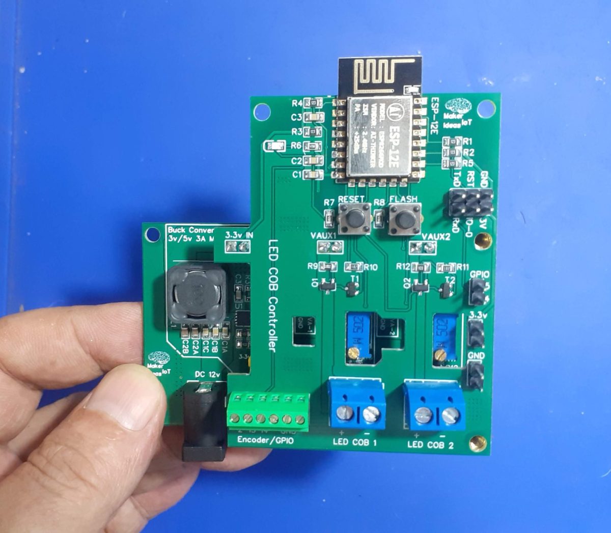
LED COB Controller stacked on top of Variable Voltage Poser Module
The second part of the project consists of a simple Custom ESP-12E PCB. Why ESP12-E? Well, I have a lot of them lying in stock, and since I won’t need any advanced features, commonly found on the bigger ESP32s, I decided to design around something that I have in stock, rather than overcomplicate the design with a bigger more advanced chip. The project features a rotary encoder, to adjust light intensity, as well as push buttons to toggle the lights on or off…
All of this is of course controlled with ESPHome. This choice gives me the option of manual or fully automatic control from HomeAssistant. It also saves me a lot of coding, as everything usually just works.
What is on the PCB?
We shall focus mainly on LED COB Controller PCB. In order to understand everything, please refer to the picture below:
LED COB controller without Power Module
The board consists of a few sections, which can be divided as follows:
ESP-12E (8266) supporting circuitry
The top area is mainly the supporting circuitry for the ESP-12E, which includes a 6-pin header to flash firmware, the classic ESP32/8266 Auto Flash/Reset circuit, and manual Flash and Reset switches. Note that the board DOES NOT contain any USB-to-Serial circuitry. I usually use those only once or twice, and update firmware OTA after that. Using an external USB-to-Serial adapter is thus sufficient for my purposes.
Power and LED Control circuitry
Power enters the board in the center, using header pins mounted on the bottom of the PCB. From left to right, these are 3.3v and then two variable voltage inputs. These all originate from the Variable voltage Power Module, mounted below the main PCB. The LED Control circuitry consists of two P-Channel Mosfets, the configuration of which was previously tested in another project, the “P-MOS MOSFET Driver Board“, also published a few weeks ago. The SI2301 P-Channel Logic Level MOSFET, used here is capable of switching up to 2.3A at 20v, and thus more than capable of handling the 300mA that the LED COB modules require.
Four cutouts are provided to access test points on the power module below, as well as the potentiometers used to set the voltage that will ultimately be sent to the LED COB Modules.
Wide copper traces connect the Mosfet’s to Screw Terminals for the LED Modules.
The Final part of the PCB is dedicated to control interfaces. A single 6-way screw terminal is provided at the bottom left corner, this is used to connect a rotary encoder, or give direct access to additional GPIO pins. On the Right hand side of the PCB, a series of header pins give access to additional 3.3v and ground connections, in addition to GPIO 4 and 5, which is usually used for I2C…
LED COB Controller stacked on top of Variable Voltage Poser Module
The Schematic
Configuration and Software
As mentioned above, this device was designed to be used with ESPHome. The configuration is thus a single YAML file and can be greatly customised to suit your exact needs…
With that in mind, I present here a VERY basic YAML file, that will toggle the LED lights on or off on pressing the encoder switch, as well as adjust the brightness by turning the encoder.
esphome:
  name: led-cob-controller
  friendly_name: LED_COB-Controller

esp8266:
  board: nodemcuv2
  restore_from_flash: True

# Enable logging
logger:

# Enable Home Assistant API
api:
  encryption:
    key: "<esphome generated>"

ota:
  password: "<esphome generated>"

wifi:
  ssid: !secret wifi_ssid
  password: !secret wifi_password

  # Enable fallback hotspot (captive portal) in case wifi connection fails
  ap:
    ssid: "Led-Cob-Controller"
    password: "<your recovery password here>"

captive_portal:

# I suggest you only copy paste from here on downwards.
# Setup the default device in ESPHome, and when it is available,
# come back and add the commands below here


text_sensor:
  - platform: wifi_info
    ip_address:
      name: IP Address
    ssid:
      name: SSID
    bssid:
      name: BSSID
    mac_address:
      name: Wifi MAC
    scan_results:
      name: WiFi Scan Results


sensor:
  - platform: adc
    pin: VCC
    name: "ESP8266 Chip Voltage"
    id: mcu_voltage
    unit_of_measurement: "V"
    device_class: "voltage"
    accuracy_decimals: 2
    update_interval: 60s
    entity_category: "diagnostic"

  - platform: wifi_signal
    name: "WiFi Signal Sensor"
    id: wifi_strength
    device_class: "signal_strength"
    unit_of_measurement: "dBm"
    update_interval: 240s
    entity_category: "diagnostic"

  - platform: copy # Reports the WiFi signal strength in %
    source_id: wifi_strength
    name: "WiFi Signal Strength"
    filters:
      - lambda: return min(max(2 * (x + 100.0), 0.0), 100.0);
    unit_of_measurement: "%"
    entity_category: "diagnostic"

  - platform: copy
    source_id: rcbright
    name: "LED Light Brightness"
    unit_of_measurement: "%"
    filters:
      - lambda: return (x * 100);

  - platform: rotary_encoder
    name: "Brightness Control"
    id: rcbright
    min_value: 0.00
    max_value: 100.00
    publish_initial_value: True
    restore_mode: RESTORE_DEFAULT_ZERO

    pin_a:
      number: GPIO13
      inverted: True
      mode:
        input: True
        pullup: True

    pin_b:
      number: GPIO2
      inverted: True
      mode:
        input: True
        pullup: True

    resolution: 1
    accuracy_decimals: 2
    filters:
    - lambda: return x / 100 ;
    on_clockwise:
    - light.control:
        id: led_light1
        brightness: !lambda |-
          // output value must be in range 0 - 1.0
          return id(rcbright).state ; // /100.0;
    - light.control:
        id: led_light2
        brightness: !lambda |-
          // output value must be in range 0 - 1.0
          return id(rcbright).state ; // /100.0;
    on_anticlockwise:
    - light.control:
        id: led_light1
        brightness: !lambda |-
          return id(rcbright).state ;
    - light.control:
        id: led_light2
        brightness: !lambda |-
          // output value must be in range 0 - 1.0
          return id(rcbright).state ; // /100.0;

binary_sensor:
  - platform: gpio
    pin: GPIO14
    id: light_switch
    name: "Light Switch"
    device_class: light
    on_click:
      then:
        - light.toggle: led_light1
        - light.toggle: led_light2


light:
  - platform: monochromatic
    name: "LED1_LIGHT_TEST"
    id: led_light1
    output: output_component1
  - platform: monochromatic
    name: "LED2_LIGHT_TEST"
    id: led_light2
    output: output_component2

# Example output entry
output:
  - platform: esp8266_pwm
    id: output_component1
    pin: GPIO12
  - platform: esp8266_pwm
    id: output_component2
    pin: GPIO16
Manufacturing the PCB
I choose PCBWay for my PCB manufacturing. Why? What makes them different from the rest?
PCBWay‘s business goal is to be the most professional PCB manufacturer for prototyping and low-volume production work in the world. With more than a decade in the business, they are committed to meeting the needs of their customers from different industries in terms of quality, delivery, cost-effectiveness and any other demanding requests. As one of the most experienced PCB manufacturers and SMT Assemblers in China, they pride themselves to be our (the Makers) best business partners, as well as good friends in every aspect of our PCB manufacturing needs. They strive to make our R&D work easy and hassle-free.
How do they do that?
PCBWay is NOT a broker. That means that they do all manufacturing and assembly themselves, cutting out all the middlemen, and saving us money.
PCBWay’s online quoting system gives a very detailed and accurate picture of all costs upfront, including components and assembly costs. This saves a lot of time and hassle.
PCBWay gives you one-on-one customer support, that answers you in 5 minutes ( from the Website chat ), or by email within a few hours ( from your personal account manager). Issues are really resolved very quickly, not that there are many anyway, but, as we are all human, it is nice to know that when a gremlin rears its head, you have someone to talk to that will do his/her best to resolve your issue as soon as possible.
This device does not need a stencil for assembly, but using one will definitely speed up things. I chose to do this build all by hand, from applying solder-paste, up to placing components.
Soldering was done on a hotplate, as usual, to reflow everything at the same time. TH components were then placed and hand-soldered.
Uploading the initial firmware, after adding the device to ESPHome was done with an external USB-to-UART converter. All further firmware changes were made via OTA.
The board performs well, with only slight heating of the LM317G variable voltage regulators on the power module when both LED COB modules are at 100% brightness. The current draw is within limits and seems to peak at about 600mA per COB…
Conclusion
This project took quite a while to move from idea to practical reality, mainly due to being busy with other more important stuff. In the end, I am happy that I sat down and did it, because it definitely will become a valuable tool in my work area.
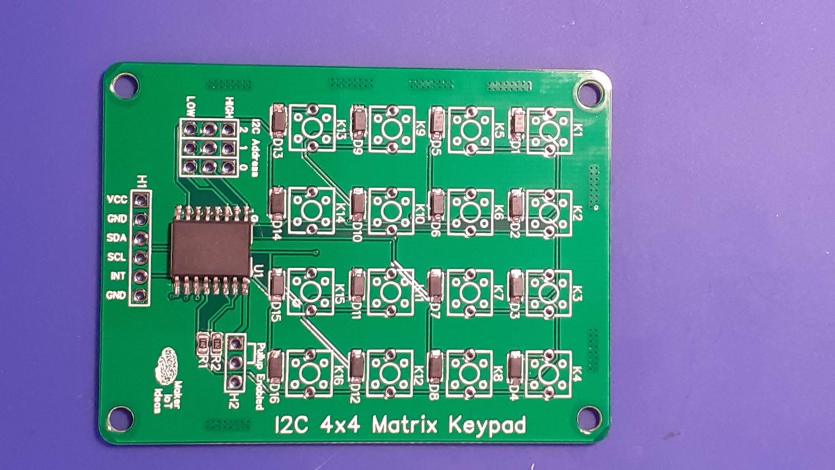
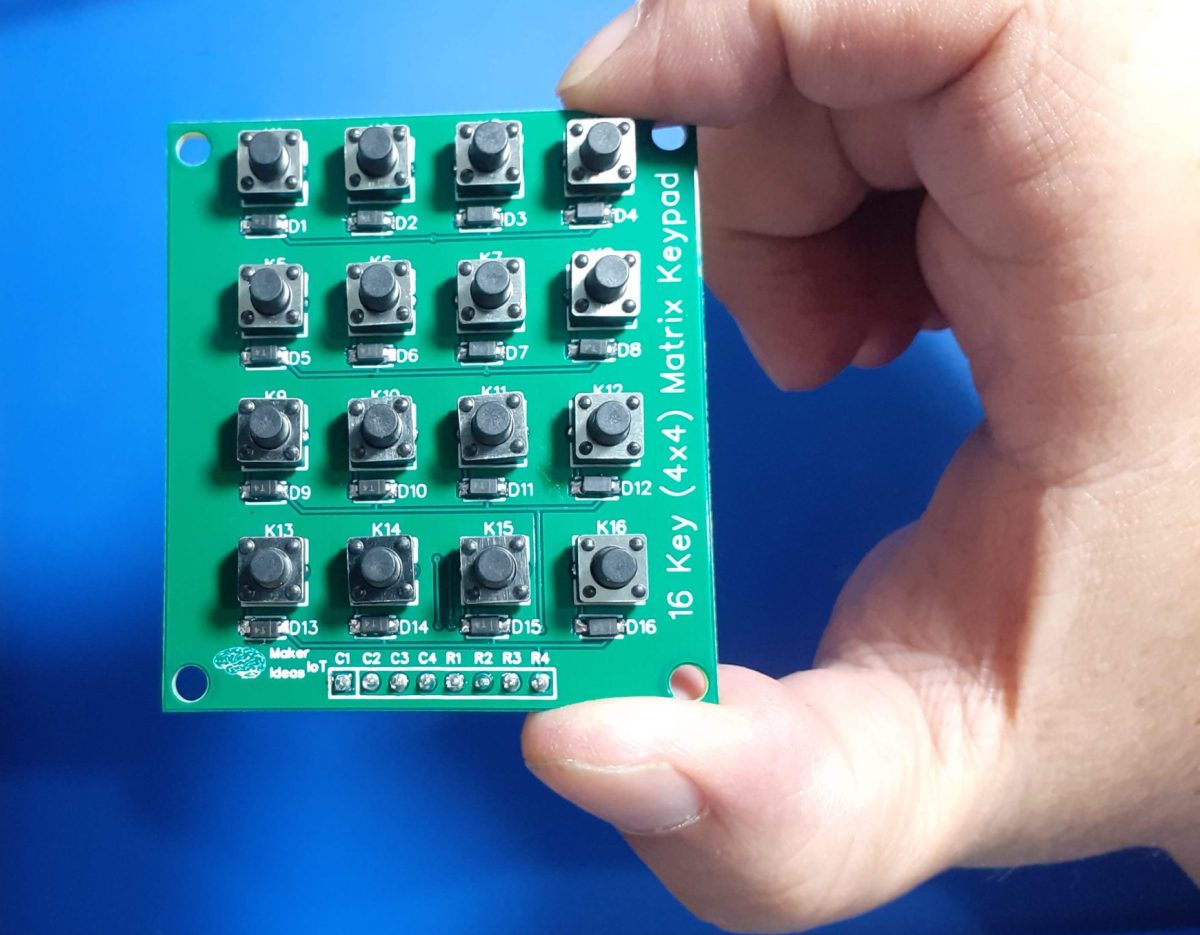
In a previous post this month I introduced my 4×4 matrix keypad. That keypad was designed to be directly interfaced to a microcontroller’s GPIO pins or alternatively to an IO expander chip like the PCF8574. That design, while working very well had the problem of requiring 8 GPIO pins to function correctly.
GPIO pins on a microcontroller can be considered very precious resources, and it should then be logical to assume that we should find a way to use these GPIO pins in a more conservative way, to allow us to interface more peripherals.
I solved this problem by integrating the keypad with an IO Expander on the same PCB. That will allow us to get away with using only 2 GPIO pins, and also open up the option of adding more keypads to the I2C bus, in the event that we need that many keys for a particular project.
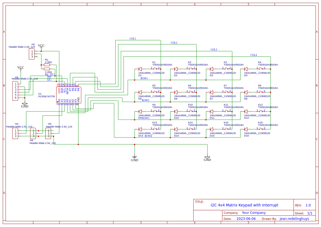
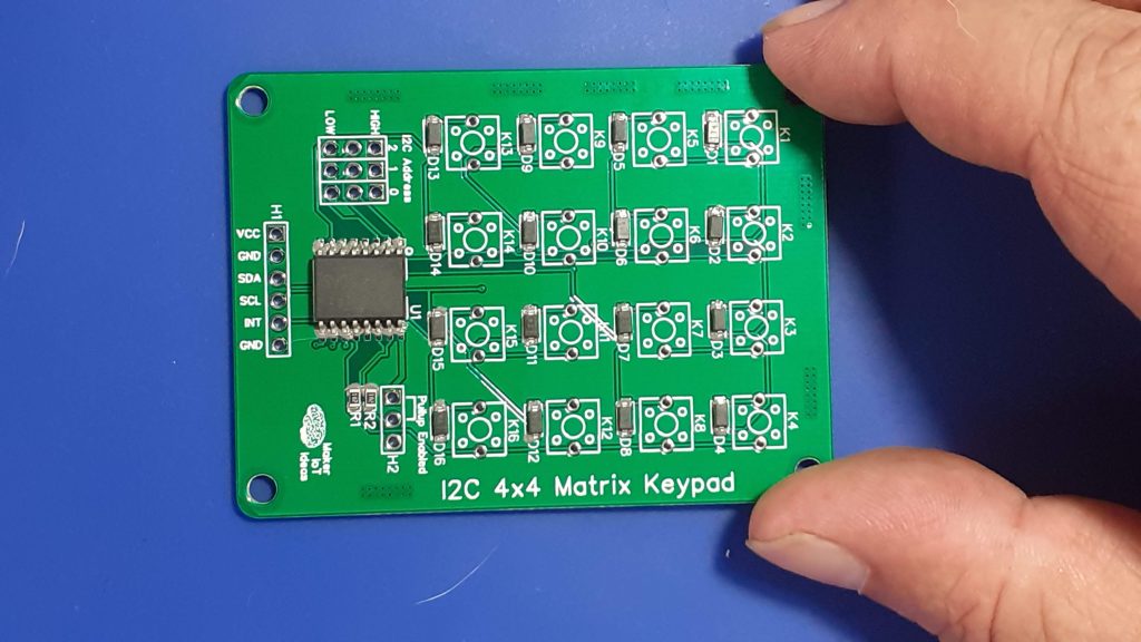
The Schematic
I2C 4×4 Matrix Keypad Schematic
Looking closely at the schematic, we can see that it is exactly the same basic keypad circuit that I used in the initial design. The only difference is that in this design, I have integrated a PCF8574 directly onto the PCB.
Some additional features include selectable I2C Pullup resistors ( usually my microcontroller development boards already include those) that can be activated with a jumper when needed. There are also a set of address selection jumpers, making it possible to stack keypads together into a bigger keyboard if you require something like that. Note that, in this version of the hardware, I did not include headers for stacking.
The keypad can be powered by a DC power source of 3.3v to 5v.
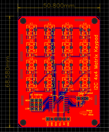
The PCB
I2C Keypad PCB
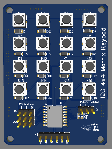
3D Render of the I2C Keypad
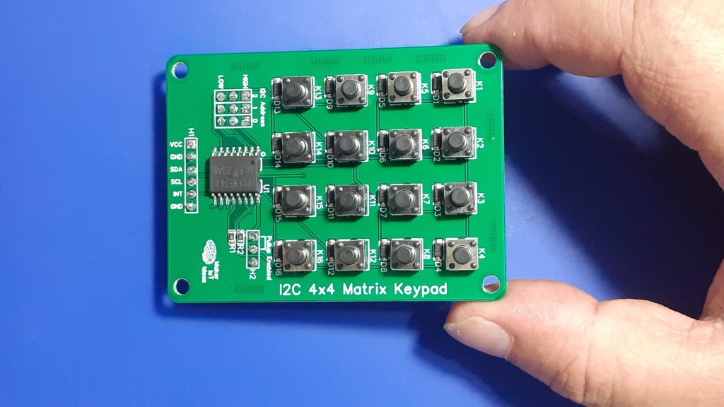
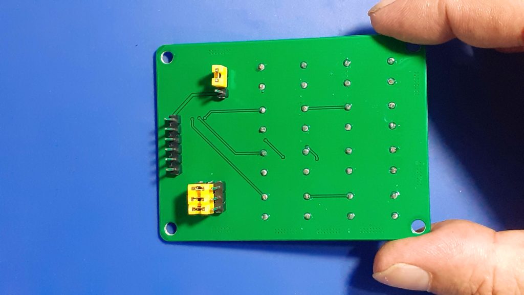
The PCB is a double-layer board of 68.8mm x 50.8mm. Male header pins provide access to the connections as well as address and pullup resistor jumpers. In my build, I have mounted these male headers on the back of the PCB. That makes it possible to mount the Keypad in an enclosure without having the jumpers “stick out” and get in the way.
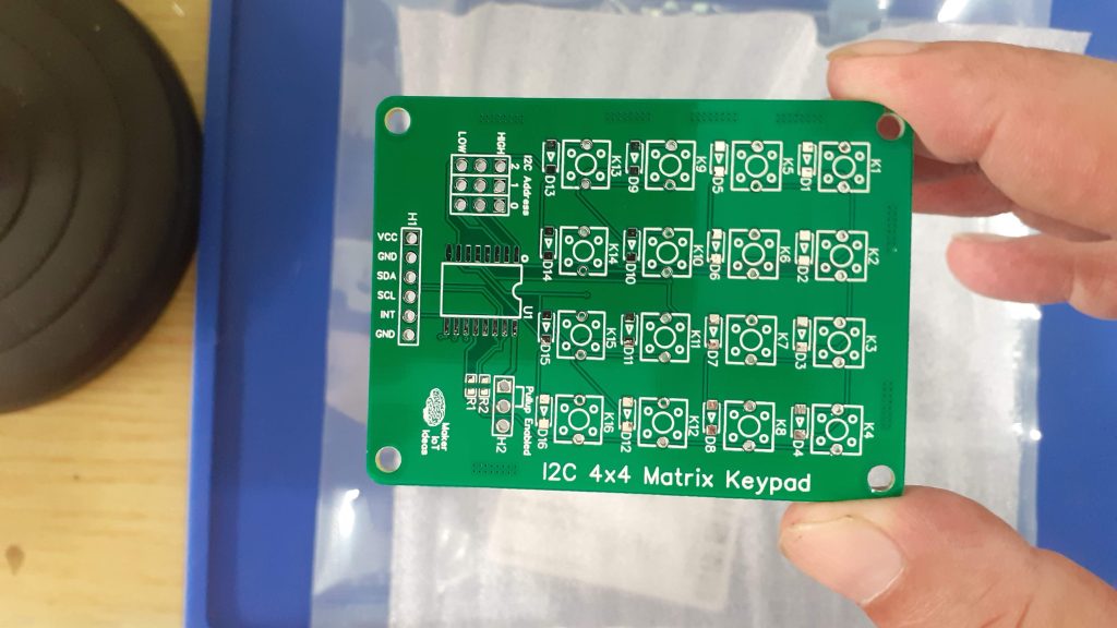
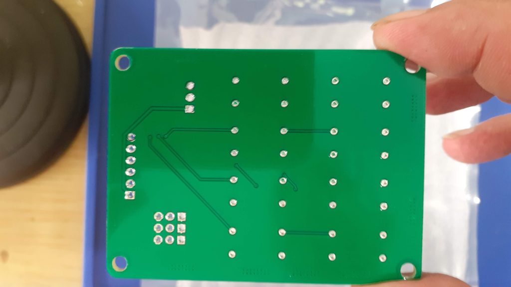
The top layer of the I2C Keypad PCBBottom Layer
Manufacturing
I choose PCBWay for my PCB manufacturing. This month, PCBWay is also celebrating its 9th anniversary, and that means that there are quite a lot of very special offers available.
Why? What makes them different from the rest?
PCBWay‘s business goal is to be the most professional PCB manufacturer for prototyping and low-volume production work in the world. With more than a decade in the business, they are committed to meeting the needs of their customers from different industries in terms of quality, delivery, cost-effectiveness and any other demanding requests. As one of the most experienced PCB manufacturers and SMT Assemblers in China, they pride themselves to be our (the Makers) best business partners, as well as good friends in every aspect of our PCB manufacturing needs. They strive to make our R&D work easy and hassle-free.
How do they do that?
PCBWay is NOT a broker. That means that they do all manufacturing and assembly themselves, cutting out all the middlemen, and saving us money.
PCBWay’s online quoting system gives a very detailed and accurate picture of all costs upfront, including components and assembly costs. This saves a lot of time and hassle.
PCBWay gives you one-on-one customer support, that answers you in 5 minutes ( from the Website chat ), or by email within a few hours ( from your personal account manager). Issues are really resolved very quickly, not that there are many anyway, but, as we are all human, it is nice to know that when a gremlin rears its head, you have someone to talk to that will do his/her best to resolve your issue as soon as possible.
The assembly of this PCB was quite easy and quick. A stencil is not required. All SMD components are 0805 or bigger. It would thus be quite easy to solder them all by hand with a fine-tipped soldering iron.
I have however used soldering paste and hot air to reflow the components, as it is the fastest, in my opinion, and definitely looks neater than hand soldering.
After placing SMD components onto solder paste – ready for reflow solderingAfter Reflow soldering with Hot Air
The board is now ready to solder the switches and header pins in place. As already mentioned above, I chose to assemble the headers on the back of the PCB to prevent them from interfering with any enclosure that I may later use with the keypad.
Final AssemblyNote that I assembled the headers onto the back of the PCB.
Testing and Coding
Testing the keypad consisted of a few steps, the first of which was ensuring that there were no short circuits, as well as that all the momentary switches worked. This was done with a multimeter in continuity as well as diode mode, with probes alternatively on each column and row in turn, while pressing the buttons.
The next stage was testing the I2C IO Expander. This was done with a simple I2C Scanning sketch on an Arduino Uno. It did not do a lot, but, I could see that the PCF8574 is responding to its address and that the pullup resistors work when enabled. This test was repeated with my own ESP8266 and ESP32 boards, this time with pullup resistors disabled, as these boards already have them onboard.
Coding came next, and it was another case of perspectives. It seems like all commercial keypads do not have diodes. This affects the way that they work with a given library. It seems that software developers and hardware developers have different understandings of what a row and a column is.
This meant that, due to the fact that I have diodes on each switch, and the way that the library work – which pins are pulled high and which are set as inputs -, I had to swap around my rows and columns in the software to get everything to work. On a keypad with the diodes replaced with 0-ohm links, that was not needed.
A short test sketch follows below:
Note that with was run on an ESP8266-12E, therefore the Wire.begin() function was changed to Wire.begin(4,5); in order to use GPIO 4 and GPIO 5 for I2C
Another point to note is that the keypad Layout will seem strange. Remember that this is due to the diodes in series on each switch. That forces us to swap around the Rows and the Columns in the software, resulting in a mirrored and rotated left representation of the keypad. It looks funny, but believe me, it actually still works perfectly.
#include <Wire.h>
#include "Keypad.h"
#include <Keypad_I2C.h>

const byte n_rows = 4;
const byte n_cols = 4;

char keys[n_rows][n_cols] = {
    {'1', '4', '7', '*'},
    {'2', '5', '8', '0'},
    {'3', '6', '9', '#'},
    {'A', 'B', 'C', 'D'}};

byte rowPins[n_rows] = {4, 5, 6, 7};
byte colPins[n_cols] = {0, 1, 2, 3};

Keypad_I2C myKeypad = Keypad_I2C(makeKeymap(keys), rowPins, colPins, n_rows, n_cols, 0x20);

String swOnState(KeyState kpadState)
{
    switch (kpadState)
    {
    case IDLE:
        return "IDLE";
        break;
    case PRESSED:
        return "PRESSED";
        break;
    case HOLD:
        return "HOLD";
        break;
    case RELEASED:
        return "RELEASED";
        break;
    } // end switch-case
    return "";
} // end switch on state function

void setup()
{
    // This will be called by App.setup()
    Serial.begin(115200);
    while (!Serial)
    { /*wait*/
    }
    Serial.println("Press any key...");
    Wire.begin(4,5);
    myKeypad.begin(makeKeymap(keys));
}

char myKeyp = NO_KEY;
KeyState myKSp = IDLE;
auto myHold = false;

void loop()
{

    char myKey = myKeypad.getKey();
    KeyState myKS = myKeypad.getState();

    if (myKSp != myKS && myKS != IDLE)
    {
        Serial.print("myKS: ");
        Serial.println(swOnState(myKS));
        myKSp = myKS;
        if (myKey != NULL)
            myKeyp = myKey;
        String r;
        r = myKeyp;
        Serial.println("myKey: " + String(r));
        if (myKS == HOLD)
            myHold = true;
        if (myKS == RELEASED)
        {
            if (myHold)
                r = r + "+";
            Serial.println(r.c_str());
            myHold = false;
        }
        Serial.println(swOnState(myKS));
        myKey == NULL;
        myKS = IDLE;
    }
}
Conclusion
This project once again delivered what I set out to achieve. It has some quirks, but nothing serious. Everything works as expected, both in the Arduino IDE/platform IO realm, as well as in ESPHome. It is worth noting that in ESPHome, we do not need to swap the rows and columns to use the Keypad component. Do remember to leave the has_diodes flag to false though…
A matrix keypad is a type of keypad that uses a matrix of wires to connect the keys to the microcontroller. This allows for a smaller and more compact keypad than a traditional keypad, which uses a single row and column of wires for each key. Matrix keypads are also more reliable than conventional keypads, as they are less susceptible to damage from dirt and moisture.
How does a matrix keypad work?
A matrix keypad is made up of a number of rows and columns of keys. Each key is connected to two wires, one for the row and one for the column. When a key is pressed, it completes a circuit between the row and column wires. The microcontroller can then determine which key is pressed by checking which row and column wires are connected.
Why use a matrix keypad?
There are a number of reasons why you might want to use a matrix keypad in your project. Here are a few of the most common reasons:
Smaller size and footprint.
Reliability.
Cost savings.
What makes my design different from most others out there?
While the matrix keypad in its simplest form is constructed from only wires and switches, that simple approach can sometimes have some unwanted effects, especially when pressing multiple keys at the same time – a phenomenon called ghosting – where you get phantom keypresses. This is easily eliminated by adding a diode in series with each switch, usually on the row connection.
That single component fixes ghosting reliably but does not come without its own problems, the most important of these being that a keypad with diodes becomes “polarised” – current can only flow in a single direction through a switch. This can cause problems with some third-party libraries, as the designer of the keypad and the designer of the library very often has quite different ideas of what a row and a column mean in a keypad.
This is important, – here we go down the rabbit hole; in my understanding of the keypad scanning routine, a column runs from top to bottom, and a row from left to right. Keeping this in mind, the microcontroller will alternatively set each column HIGH, and configure each row as an input. When a key is pressed, current will flow from the specific column GPIO, through the switch, and into the Row GPIO, sending the input pin HIGH…
It is also possible to configure the columns as inputs, with internal pullups enabled, and have each Row pin as an output, configured to sink ( pull current to ground). This will cause the specific column to go low – thus identifying the pressed key…
These different ways of handling the problem of reading a key, and believe me, there are actually more variations, create a few unique problems. We may have to swap rows and columns as far as pin connections and firmware are concerned, as well as define a custom “keymap” to assign values to each key.
The Schematic
As we can see above, the schematic is very basic. 16 switches, 16 diodes and a single 8-way header pin. Pin 1 to 4 on the header is connected to Columns 1 to 4, and Pin 5 to 8 is connected to Rows 1 to 4.
The diodes prevent “ghosting currents from flowing into other keys in a row when multiple keys are pressed together. They also seem to help with other stray signals and interference.
The PCB
The PCB is a simple double-layer board. All components are mounted on the top layer.
To limit interference from stray signals, I have routed rows and columns on opposite sides of the PCB where possible.
Manufacturing
I choose PCBWay for my PCB manufacturing. This month, PCBWay is also celebrating its 9th anniversary, and that means that there are quite a lot of very special offers available.
Why? What makes them different from the rest? PCBWay‘s business goal is to be the most professional PCB manufacturer for prototyping and low-volume production work in the world. With more than a decade in the business, they are committed to meeting the needs of their customers from different industries in terms of quality, delivery, cost-effectiveness and any other demanding requests. As one of the most experienced PCB manufacturers and SMT Assemblers in China, they pride themselves to be our (the Makers) best business partners, as well as good friends in every aspect of our PCB manufacturing needs. They strive to make our R&D work easy and hassle-free.
How do they do that?
PCBWay is NOT a broker. That means that they do all manufacturing and assembly themselves, cutting out all the middlemen, and saving us money.
PCBWay’s online quoting system gives a very detailed and accurate picture of all costs upfront, including components and assembly costs. This saves a lot of time and hassle.
PCBWay gives you one-on-one customer support, that answers you in 5 minutes ( from the Website chat ), or by email within a few hours ( from your personal account manager). Issues are really resolved very quickly, not that there are many anyway, but, as we are all human, it is nice to know that when a gremlin rears its head, you have someone to talk to that will do his/her best to resolve your issue as soon as possible.
This project does not require a lot of specialised equipment to assemble. The SMD diodes can easily be soldered by hand, the same with the switches and 8-way header. In my case, I chose to solder the header pins on the back of the PCB, that way, I can later use the keypad in a suitable enclosure without having wires in the way.
Testing and Coding
Testing a matric keypad can sometimes be a challenge. In my case, a multimeter with clip leads, set to diode mode, with the leads connected to each column and row in turn, while minding the polarity, and pressing each key in that row in turn, verified continuity.
With that done, it was time to put my trusted Cytron Maker Uno to work, as this Arduino Clone has the added benefit of having LEDs on each of the GPIO lines, thus making it very easy to see what is happening.
I made use of a Keypad library in the Arduino IDE, mainly to cut down on the amount of coding, but also because it is easier to use a working piece of code, and then adapt that to my keypad.
Detailed Code examples for ESPHome are available on Patreon
/* @file CustomKeypad.pde || @version 1.0 || @author Alexander Brevig || @contact alexanderbrevig@gmail.com || || @description || | Demonstrates changing the keypad size and key values. || #
Edited by MakerIoT2020, with minor changes to make it function correctly with my custom keypad. I have also added a simple LED blinking routine to show that the Arduino is “alive” and that the Keypad code seems to be NON-blocking – which is quite important to me.
*/ #include <Keypad.h>
const byte ROWS = 4; //four rows const byte COLS = 4; //four columns //define the symbols on the buttons of the keypads char hexaKeys[ROWS][COLS] = { {‘1′,’4′,’7′,’*’}, {‘2′,’5′,’8′,’0’}, {‘3′,’6′,’9′,’#’}, {‘A’,’B’,’C’,’D’} }; byte rowPins[ROWS] = {2,3,4,5}; //connect to the row pinouts of the keypad byte colPins[COLS] = {6,7,8,9}; //connect to the column pinouts of the keypad /* * Due to libraries being written by different people, and our definitions about * what a row and a column are, is different, note that the rows in the code * is actually the columns on my PCB. This becomes true, due to the fact that my * PCB has Diodes on each switch, and that thus makes current flow in only one * direction/// * * it also has the “side effect” that keys are layout in a strange “mirrored” and * rotated way in the firmware. * it does however NOT affect the correct operation of the Keypad Module at all * */
const int LEDPin = LED_BUILTIN; int ledState = LOW; unsigned long prevmillis = 0; const long interval = 1000;
//initialize an instance of class NewKeypad Keypad customKeypad = Keypad( makeKeymap(hexaKeys), rowPins, colPins, ROWS, COLS);
This code works very well and allowed me to verify the correct operation of the keypad.
In conclusion
Making my own Keypad Module is a project that is long overdue. I have purchased a few online over the years, and as they were mostly of the membrane type, they did not last very long – it must be something to do with the ultra-cheap flexible PCB ribbon connector, since a quality membrane keypad can be quite expensive, and usually lasts quite a long time.
Having my own module available to experiment with will allow me to do some long-delayed improvements to many of my IoT modules. That code, mostly YAML for ESPHome, will be made available on Patreon.
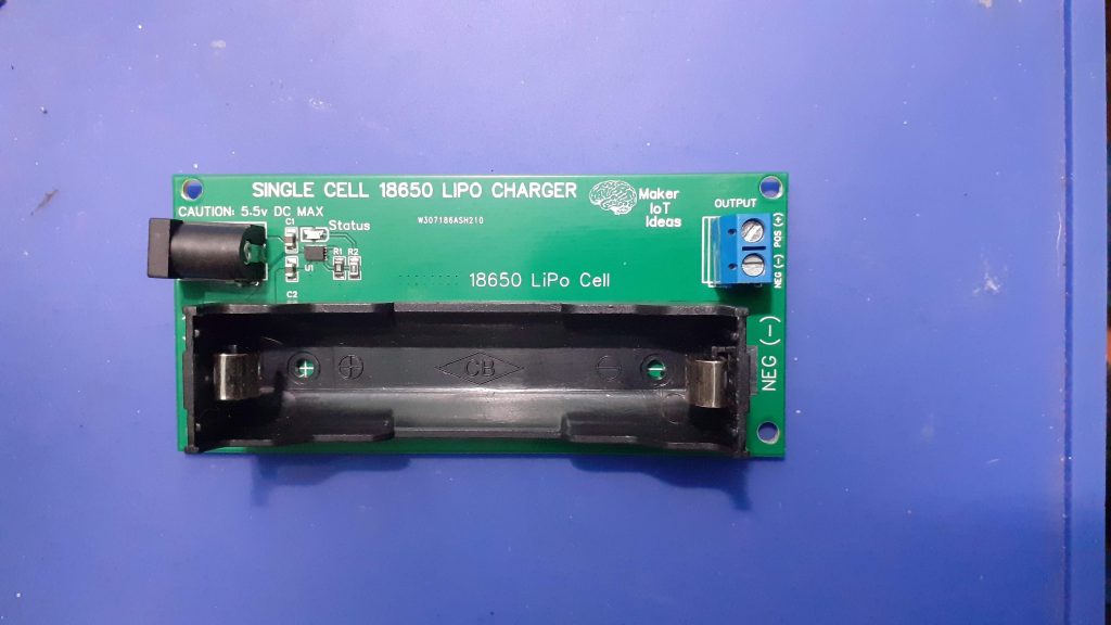
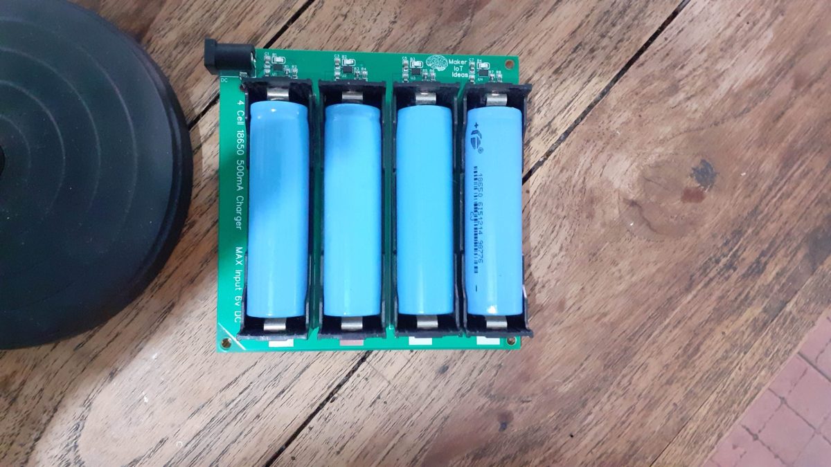
Due to their high capacity and relatively low cost, LiPo cells are almost everywhere these days. This Low BOM cost 4-cell 18650 Charger module is my attempt to solve another issue.
The 18650 Lipo cell is quite common in my lab, and for an excellent reason, as mentioned above, they are cost-effective and also store quite a bit of energy. recharging them after use has however been quite a lengthy exercise in the past.
The usual process involved a few Lipo Charging modules, all connected via USB cables, charging one cell at a time. This not only takes up quite a bit of time and space but also occupies USB ports that could be used for other purposes.
Based on the ultra-cheap TP4056 chip, these single-cell charging modules cost peanuts, but with the required wiring and battery holders, as well as the cables to supply power, it does not really look very neat. I have thus been looking for a better solution for quite a while now, and had quite a few requirements for my “ideal” module.
The MCP73832 from MICROCHIP seemed like a good choice for a custom design, as it requires only 5 additional external components, which are only two resistors, two capacitors and an led. The chip is also extremely low-cost.
High accuracy preset output voltage regulation (+/-0.75%)
Output voltage options include 4.2V, 4.35V, 4.4V and 4.5V
User-programmable charge current
Open-drain status output
On-chip thermal regulation
Preconditioning and end-of-charge ratio options
Under-voltage lockout
Includes integrated pass transistor, integrated current sensing, and reverse discharge protection in 5-pin SOT-23 and thermally-efficient 8-pin 2mm x 3mm DFN packages.
The Prototype Module
The design that I came up with, can charge 4-cell simultaneously. The maximum input voltage is limited to 6v DC.
Another interesting feature is the ability to use either through-hole battery holders or SMD ones. I did that because I have quite a few of the through-hole ones in stock, but as they were bought quite a while ago, the exact part number went on holiday. When having the module assembled in the factory,the SMD parts can be used, as there seems to be plenty in stock.
The Schematic
Because I enjoy a challenge, the design uses the smaller 3mm 2mm DFN8 package. Charging current is set with R9, which is 2k in this case, which will result in a charging current of the full 500mA. You can adjust it as per your requirements, to a value between 2k and 10k, as per the datasheet.
The PCB design was optimised to fit on a 10cm x 10cm board. Most of the board is made up of a solid copper pour to provide a good ground plane. Charging circuitry is placed as close together as possible, with a good connection of the thermal pad on the DFN8 package to the ground plane to help with thermal regulation. In this case, I have attempted to replicate the suggested reference design as closely as possible, while adapting it for use with the DFN8 package (Reference design uses the 5 lead SOT-23 package)
As seen in the close-up, components are placed as close as possible to the MCP73832, and via stitching are used to ensure a good connection to the ground, as well as allow the ground plane to serve as a heatsink.
Manufacturing
I choose PCBWay for my PCB manufacturing. Why? What makes them different from the rest?
PCBWay‘s business goal is to be the most professional PCB manufacturer for prototyping and low-volume production work in the world. With more than a decade in the business, they are committed to meeting the needs of their customers from different industries in terms of quality, delivery, cost-effectiveness and any other demanding requests. As one of the most experienced PCB manufacturers and SMT Assemblers in China, they pride themselves to be our (the Makers) best business partners, as well as good friends in every aspect of our PCB manufacturing needs. They strive to make our R&D work easy and hassle-free.
How do they do that?
PCBWay is NOT a broker. That means that they do all manufacturing and assembly themselves, cutting out all the middlemen, and saving us money.
PCBWay’s online quoting system gives a very detailed and accurate picture of all costs upfront, including components and assembly costs. This saves a lot of time and hassle.
PCBWay gives you one-on-one customer support, that answers you in 5 minutes ( from the Website chat ), or by email within a few hours ( from your personal account manager). Issues are really resolved very quickly, not that there are many anyway, but, as we are all human, it is nice to know that when a gremlin rears its head, you have someone to talk to that will do his/her best to resolve your issue as soon as possible.
Assembly of this module definitely requires the use of a stencil. The DFN-8 package of the IC is only 3mm x 2mm, and there are 8 leads as well as a thermal pad crammed in there. A stencil will ensure that you add just the correct amount of solder paste to each pad.
As we can clearly see in this cropped picture of the stencil, those pads are SUPER tiny.
I chose to use the hotplate, as well as some hot air for the SMD component assembly. The battery holders and DC barrel-connector are all through-hole, and were thus assembled using a standard soldering iron, with slightly thicker solder, and a bit more heat than normal, as the pads are quite big, and the big copper pour really sucks the heat away from the joints.
Testing
Testing the module went really well. I used four 18650 cells that needed recharging, and they were very quickly ( in about 1 hour ) charged to 4.20 volt.
The Charge Indicator LED on each charging circuit works in reverse from what we would normally expect, with it lighting up while charging, and going out when done.
The current draw (measured on the bench power supply) verified that each cell was charging at the 500mA as designed. The current draw also reduced as each cell charging cycle completed and eventually went down to very close to zero (The Ampere meter on my bench supply can not measure very low current with a lof of accuracy -:) )
Measuring each cell that have completed its charging cycle with a standard multimeter confirmed that they were indeed at 4.20v, and that the charging circuitry was no longer feeding current to any of them.
Drawing current out of a single cell (I used a set of clips ) to power a dummy load, resulted in an automatic recharge cycle being initiated once the cell voltage dropped past the set charging threshold.
It is however VERY important to note that this module is by NO means a balanced cell charger. It is a 4-way single cell charger that charges 4 cells independently from each other, at the same time. It is thus completely possible as well as probable that the four cells will/may be at slightly different voltages at the end of each respective charging cycle.
Conclusion
This project is most definitely high on the list of my most needed items. Keeping a bunch of 18650 cells charged and correctly maintained can be quite a chore, and the way that I have done it in the past was definitively not ideal. It has also cost me quite a few cells that died way before their time.
Using this module, the chore of charging these cells will be reduced by a lot, and hopefully, in the future, I will come up with a solution to augment this module so that I can have these cells on a semi-permanent charge, with monitoring and only charging those cells that needs it.
Pictures
Closeup – Charging circuitPCB topPCB BottomCharging circuit assembled – closeup4-cell 18650 Charger, based on the MCP73832side viewFront view
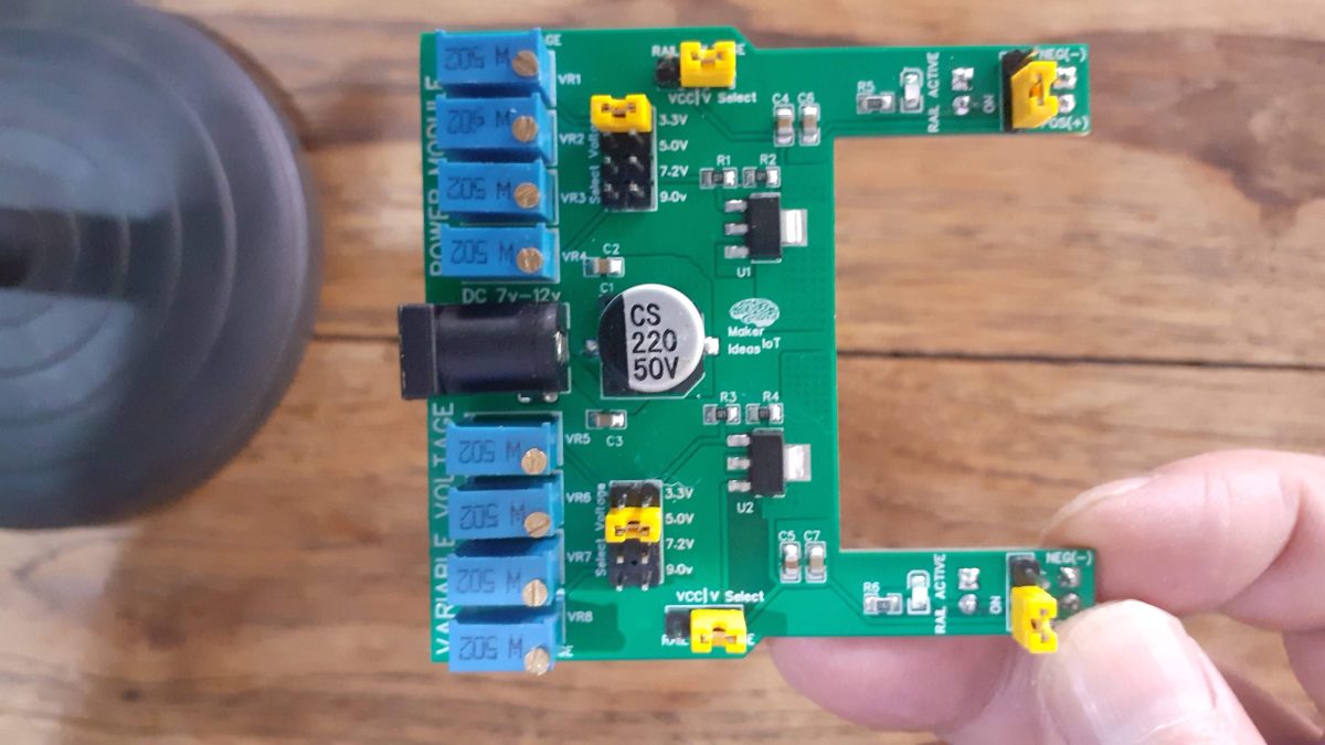
A few weeks ago, I designed and built my own breadboard power module, mainly to try and solve some perceived problems with commercial ones, and also just to have something that is completely my own.
While that design does indeed work very well, I did however find a few tiny issues that still needed attention.
Two fixed voltages, 3.3v and 5.0v
1A current limit per regulator
PCB Heatsink design can be improved further, as there is still a bit too much heat at a high current draw – not much actually, but I like things running as cool as possible.
Other requirements that popped up were the ability to have more than two set voltages, as well as being able to send the full Vsupply to a power rail if I choose to do so…
Having a few LM317G variable voltage regulators lying around, left over from a previous project, I decided to use those. They can source an additional 500mA of current (1500mA in total) and also makes it quite easy to have variable voltages.
Voltage is set with two resistors, of which one is usually a variable resistor. This does however mean that you need a multimeter or other device capable of measuring voltage each time that you need a different voltage, as well as to determine at what voltage the device is currently set if you have not used it in a while…
The initial prototype is quite bulky at the moment, but I do plan to change that in the future when I am completely happy with the performance of the module
Each “voltage channel” consists of a 5k multiturn “trim pot” that connects back through a selectable jumper to a 240-ohm resistor ( I actually used two precision 120-ohm resistors in series) on the adjust pin of the regulator.
I have also reduced the number of smoothing capacitors on the input and outputs, as the voltages are quite stable
After assembly, it only takes a few minutes to adjust each “trim pot” to the correct value using a small screwdriver and a multimeter. Once set and verified, they can be locked using a drop of “lock-tight” or similar.
The eight “trim pots” sets the voltages as follows:
Turning the “pot” anti-clockwise reduces the voltage, while a clockwise movement increases it.
Changing voltages then becomes as easy as changing a jumper to a preset position.
The Schematic
As mentioned above, I have used two precision 120-ohm resistors on one leg of the resister divider that is connected to the adjust leg. Feel free to replace that with a single 240-ohm resistor and a 0-ohm bridge.
The multiturn precision 5k trim pots give great control and the desired voltages can be dialled in very accurately.
The module was designed as a double-layer PCB. I used big solid ground planes to provide good grounding, as well as serve as heat sinks for the voltage regulators.
Manufacturing
I choose PCBWay for my PCB manufacturing. Why? What makes them different from the rest?
PCBWay‘s business goal is to be the most professional PCB manufacturer for prototyping and low-volume production work in the world. With more than a decade in the business, they are committed to meeting the needs of their customers from different industries in terms of quality, delivery, cost-effectiveness and any other demanding requests. As one of the most experienced PCB manufacturers and SMT Assemblers in China, they pride themselves to be our (the Makers) best business partners, as well as good friends in every aspect of our PCB manufacturing needs. They strive to make our R&D work easy and hassle-free.
How do they do that?
PCBWay is NOT a broker. That means that they do all manufacturing and assembly themselves, cutting out all the middlemen, and saving us money.
PCBWay’s online quoting system gives a very detailed and accurate picture of all costs upfront, including components and assembly costs. This saves a lot of time and hassle.
PCBWay gives you one-on-one customer support, that answers you in 5 minutes ( from the Website chat ), or by email within a few hours ( from your personal account manager). Issues are really resolved very quickly, not that there are many anyway, but, as we are all human, it is nice to know that when a gremlin rears its head, you have someone to talk to that will do his/her best to resolve your issue as soon as possible.
The assembly of this module is quite easy, no stencil is required. I recommend that you take care of the SMD components first, using hot -air or even hand soldering them, before assembling the through-hole components.
Here I do recommend that you use a breadboard to make sure that the 2.54mm headers that will connect to the power rails are lined up nicely
Testing and Setup
As already described above, the module does require a bit of setup after assembly. To do this, you will require a DC power supply with a voltage of 7v to 12v, as well as a multimeter, preferably with clips on the test leads, as well as a small terminal screwdriver.
With the module powered, and the Rail Voltage jumpers set to VCC, measure the rail outputs with the multimeter ( remember that the rail active jumper MUST be set to on). Both rails should be at the same voltage as your VCC input voltage, ie 12v DC
Move the Select Voltage jumper for both rails to the 3.3v position, and the Rail voltage jumper to the VSelect position for both rails.
With the multimeter connected to each rail in turn, turn VR1 anti-clockwise until the voltage for the top rail is set to 3.3v. Repeat for the bottom rail, adjusting VR5 instead, while measuring the bottom rail.
Repeat this step for each of the voltages, remember to power off the module before changing jumper positions – to prevent accidental short circuits…
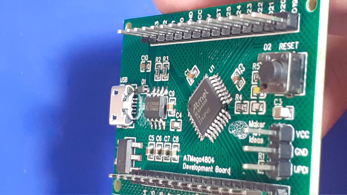
The ATMEGA4808 provides a very attractive solution to replace the trusted ATMEGA328 or standard Arduino UNO /NANO.
These chips are slightly more difficult to get hold of than the ATTiny chips, and cost a little bit more ( about the same as what the ATMEGA328 used to cost before the mess with COVID-19 and resulting supply chain shortages + inflated costs), but they offer all of the functions of the ATMEGA328, with a few other enhancements that will definitely be very useful.
The extras include: – Hardware interrupts on ALL GPIO pins; This is way more than the standard 2 interrupts on the ATMEGA328 ( We are not talking about the Pin Change interrupts, but real hardware interrupts, that can be triggered on RISING, FALLING, CHANGE, HIGH and LOW state of each pin
– Up to eight (8) PWM pins as opposed to the 6 on the Arduino UNO – Up to eleven Analog inputs – An Analog Comparator module – Configurable Custom Logic (CCL) – EVENT System (EVSYS) – Peripheral pin swapping
It is also worth mentioning that these chips have accurate internal oscillators, capable of clocking the chip at up to 20MHz, further reducing the number of external components required to get a minimal configuration running…
While I have had a Nano Every “Clone” lying in a drawer for quite a while now, I did not really pay a lot of attention to it. That was, until I needed an ATMEGA328 for a project, and could not find any for sale, or at least at a price that I was willing to pay for it… That incident was the spark that ignited this entire exercise, to find a suitable replacement…
The Nano Every “Clone” in my possession, used the ATMEGA 4808 chip and turned out to be the Thinary Nano 4808. I had quite a lot of problems with the provided core, as well as getting peripherals like I2c and SPI to work. This led to further investigations, and finally, I decided on building my own and to use the MCUdude/MegaCoreX Arduino Core to program it.
This led to the following prototype:
ATMEGA4808 Development board prototype
I did not bother with too much detail on the silk screen here, as the goal was to get a working board, test it, and then later, design a refined PCB.
What is important to note is that the board runs at 5v, but provides a single 3.3v output as well. Logic levels on the GPIO is also 5v. Use level converters for 3.3v only addons…
The MEGA4808 is programmed via UPDI, so we have a UPDI Header on the right-hand side of the PCB. It is also possible to use the Optiboot Bootloader, to flash the board in true Arduino style through a USB connection to a computer.
A CH340N USB-to-Serial converter chip is used instead of the CH340G that is common on the UNO clones. The CH340N provides only the USB D+ D- signals, as well as Rx, TX and RTS. RTS is being used to auto-reset the chip after flashing…
In comparison to the CH340G, which also required a crystal oscillator, but provides all the modem control signals, which, are usually not even broken out, the CH340N made much more sense.
PCB Bottom.
A power LED, as well as an indicator LED on pin 7 was also included.
Assembled PCB, Top Layer.
Assembly and Soldering
I normally assemble all my projects by hand and reflow-solder them with a hot plate. for this project, I decided to do things a bit differently, which ended up being a bit awkward, but still resulted in a perfectly useable PBC.
As you will know by now, I only do written articles, as I don’t consider myself ready for the Youtube and video thing, as well as because I believe a well-written article, with detailed pictures, is easier to understand than a video…
Well, today, we will have both… This article, with its writeups and pictures, as well as a short assembly and soldering video, with no sound, sped up 5x, as I did not want to bore anyone with a 25-minute silent video…
Let us begin then…
PCB and Stencil
We start with a blank PCB and the laser-cut stainless steel stencil that I got from PCBWay.
Solder paste applied
Solder paste is then applied with the stencil and a scraper, and afterwards, the stencil is removed… The PCB is now ready for component placement…
From here on, we will go to the video footage… showing component placement, with some awkwardness due to the camera being in the way, as well as hot-air soldering, with the same awkwardness, as I was forced to use my right hand ( I am left-handed), not to block the camera view…
https://youtu.be/Lr_eWPD2XgA
Begin quite new to the video thing, I have also not quite figured out the editing software, so the video is in native resolution… not zoomed…
After assembly
After assembly, I checked for solder bridges and was quite happy that there were none. This also meant that the board worked perfectly the first time around… as it should…
I choose PCBWay for my PCB manufacturing. Why? What makes them different from the rest?
PCBWay‘s business goal is to be the most professional PCB manufacturer for prototyping and low-volume production work in the world. With more than a decade in the business, they are committed to meeting the needs of their customers from different industries in terms of quality, delivery, cost-effectiveness and any other demanding requests. As one of the most experienced PCB manufacturers and SMT Assemblers in China, they pride themselves to be our (the Makers) best business partners, as well as good friends in every aspect of our PCB manufacturing needs. They strive to make our R&D work easy and hassle-free.
How do they do that?
PCBWay is NOT a broker. That means that they do all manufacturing and assembly themselves, cutting out all the middlemen, and saving us money.
PCBWay’s online quoting system gives a very detailed and accurate picture of all costs upfront, including components and assembly costs. This saves a lot of time and hassle.
PCBWay gives you one-on-one customer support, that answers you in 5 minutes ( from the Website chat ) , or by email within a few hours ( from your personal account manager). Issues are really resolved very quickly, not that there are many anyway, but, as we are all human, it is nice to know that when a gremlin rears its head, you have someone to talk to that will do his/her best to resolve your issue as soon as possible.


