
In a previous post, I designed a breadboard-friendly MCP23017 breakout module. A few months have passed, and after using the module for a while, some issues came to light…
In this post, I will show you how I have fixed those issues, and then I can continue testing/using the new generation prototype, and hopefully, it can become the final revision of this project.
Old Versus New
Let us start by looking at the old and new PCB designs…


There will not be a lot of obvious differences at first, but if we look closely, here are the changes:
– In the old version, due to the size of the SOIC28 footprint, I had to place the bypass capacitors, as well as I2C pullup resistors on the bottom layer of the PCB.
- The new design, using the more readily available ( at least where I live) SSOP28 footprint, leaves enough space for these components on the top layer, thus resulting in a mostly single-layer layout, with only a few tracks on the bottom layer.
- I2C pull-up resistors can now be controlled by a jumper, enabling or disabling them completely… This helps when adding a few devices to the I2C bus, and rather having the pull-up’s close to the MCU ( as is generally recommended anyway )
- Other cosmetic changes involve the separation of the data ports (A and B) from the interrupts, reset, Vcc and ground pins. On initial testing of this on a breadboard, it makes using the device a bit easier, and access to the io pins faster. ( In my biased opinion anyway )

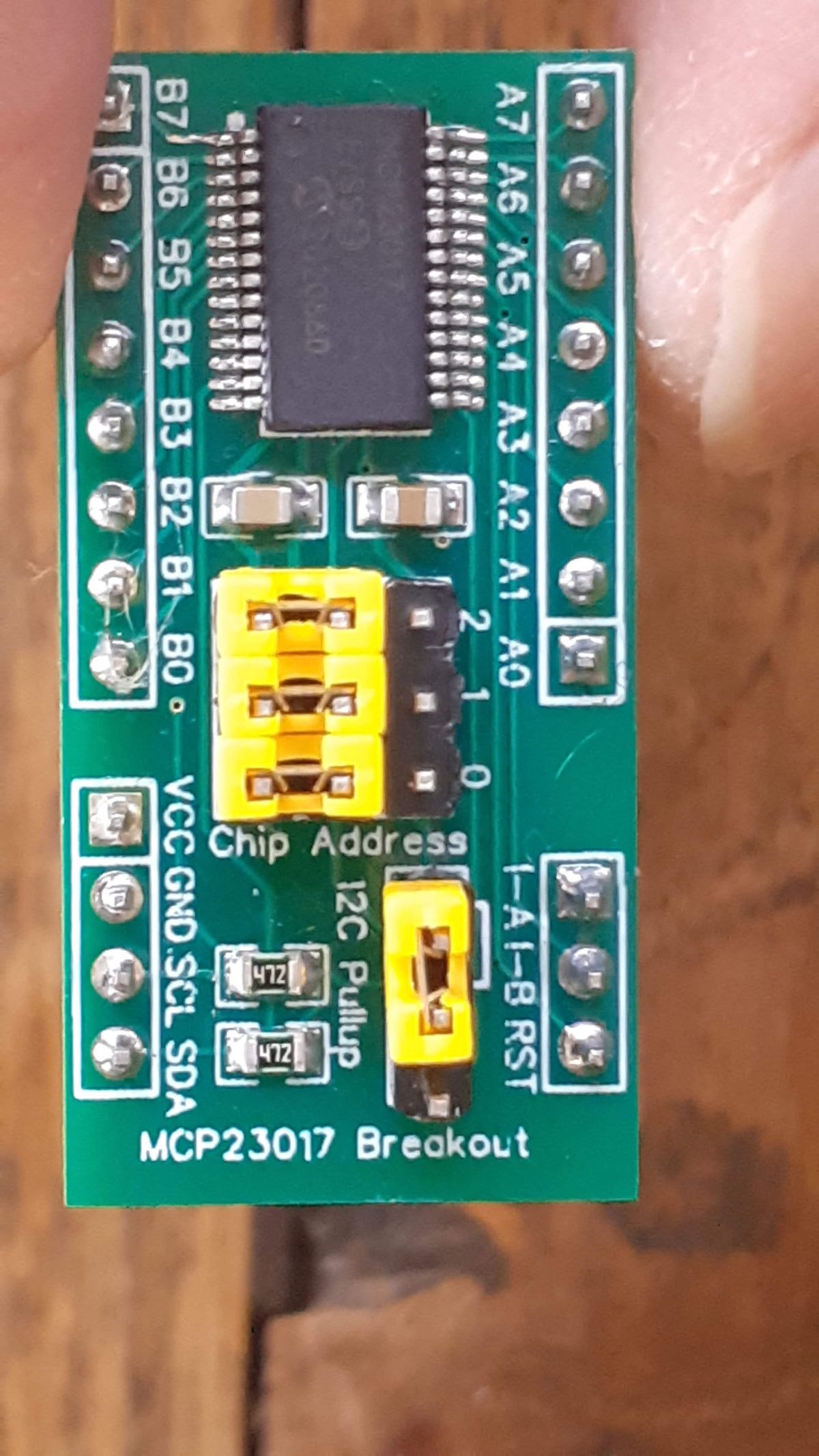
Pinouts and connections
I have tried to make all the connections easy to find and use, with the IO ports ( A and B) on opposite sides of the breakout, Numbered A7 to A0 on the top, and B7 to B0 on the bottom.
VCC, GND, SCL and SDA are on a separate 4-way header pin, with the two interrupt pins (I-A and I-B) together with the reset (RST) pin on a 3-way header opposite the power and signal header..
Addressing pins are in the centre of the PCB, marked with a 2 1 0 ( for AD2, AD1, and AD0 respectively), Jumpers to the bottom ( towards port B) pull the pins to ground, where the opposite side will pull the address pins high.
To the right of that, another 3-way jumper enables or disables the I2C pull-resistors on the module, which in this case is set at 4k7.
Manufacturing
The PCB for this project has been manufactured at PCBWay.
Please consider supporting them if you would like your own copy of this PCB, or if you have any PCB of your own that you need to have manufactured.

Some More Pictures


