
While prototyping our projects, we Makers often need to interface devices with a higher current draw, like motors, or RGB lights, to our microcontrollers. These typically are unsuitable for connecting directly to an Arduino, ESP32 or Raspberry Pi’s GPIO pins. This is usually the time when we start grabbing transistors or MOSFETs.
While I normally keep a few leaded transistors and MOSFETs in the lab, These are not always convenient to use, as they may be in big packages or have the wrong specifications for the task that we are trying to perform.
SMD versions are more common in my lab, but they come with the problem of being small, and also completely unfriendly to the breadboard environment.
I have thus been playing with an idea to make a series of dedicated breakout boards for just this purpose. Having an easy way to test a specific MOSFET for a design, and having more than one of them handy, without all the wiring issues, and using the bare minimum of those DuPont wires!

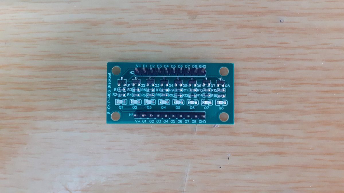
I came up with the following prototype, which, while not completely optimised yet, already makes things easier. The breakout board provides 8 P-Channel Mosfets, with a single source connection, and individually broken-out Drain and Gate pins.
LED indicators on each channel provide a visual indication of the status of each P-Mos device, and the breakout can also be mounted directly into an enclosure if needed.
What is on the PCB?
Each channel comprises a P-Channel Mosfet, in this case, a SI2301, which has a suitably low gate voltage, a pullup resistor on the gate, to keep it from floating, a status-indicating LED and a current-limiting resistor for the LED.
No gate resistor was added, as this would change depending on the actual MOSFET, as well as the microcontroller that you use. The Gate pullup resistor can also be left unpopulated, in case you need to do something specific there.
Two rows of 10-way, 2.54 header pins are at the top and bottom of the PCB, to make using the breakout on a breadboard possible.
The Pinouts are as follows
H2 – Top V+ D1 D2 D3 D4 D5 D6 D7 D8 GND
with Dx corresponding to the Drain pin of each MOSFET. All the Source pins are internally connected together, as I assumed that I will use the same source voltage on each channel anyway.
H1 – Bottom V+ G1 G2 G3 G4 G5 G6 G7 G8 GND
with Gx corresponding to the gate pin of each MOSFET.
V+ and GND for each header is internally connected, to make it possible to supply V+ and Gnd on any of the two headers.

The Schematic

Using the Breakout
Using the breakout is straightforward. Connect a source voltage to either of the V+ pins and Ground to either of the GND pins. ( the ground is used internally for the status LEDs)
Connect your load, with the positive to a drain pin, let us say D1, and the load ground to your breadboard, or power supply ground. Connect the corresponding gate pin, in our case G1, to the microcontroller pin of your choice, through a suitable gate resistor, and pull it high at setup, to ensure that the MOSFET stays off. Pull low to activate as needed.
Please note that you should not try to switch excessively large currents through a single MOSFET Channel, as the PCB traces can realistically only handle approximately 300 to 400mA per channel.
Note 2: If you are driving an inductive load, it is considered good practice to add a flywheel diode on the load as well. This will protect the MOSFET from back EMF when the MOSFET is switched off.

Manufacturing
The PCB for this project has been manufactured at PCBWay.
Please consider supporting them if you would like your own copy of this PCB, or if you have any PCB of your own that you need to have manufactured.

Example code for using the breakout (Arduino)
// Declare Gate driving GPIO pins
int gate1 = 10;
int gate2 = 11;


void setup() {
// Set the GPIO pins as outputs and drive them HIGH
// This keeps the channels switched "OFF"
  digitalWrite(gate1,HIGH);
  digitalWrite(gate2,HIGH);
  pinMode(gate1,OUTPUT);
  pinMode(gate2,OUTPUT);

// Writing to the GPIO's before setting their pin Mode,ensures that the
// GPIO's are in fact initiated in a know correct state.

  Serial.begin(115200);

}

void loop() {
// In the loop, we just toggle the GPIOs, thus
// alternatively switching the channels on or off
  digitalWrite(gate1,!digitalRead(gate1));
  digitalWrite(gate2,!digitalRead(gate1));
  delay(1000);
  }