Easy to use ESP32-S DEV Prototype Shield

While my recent ESP32-S Dev Board really does the trick to help my development cycle along, I very quickly ran into another obstacle, in the sense that, after doing stuff on the breadboard, moving those components onto a more permanent location, either as a next stage prototype or more likely that the project is so small and insignificant not to warrant the effort actually to design a PCB for it. This could be rectified by using another one of my recent designs, an SMD breadboard PCB, but that would not always do either.

MakerIoT SMD Prototype development PCB

That got me thinking, and while staring at the ever-present Arduino Uno on its corner of the work-bench, I suddenly remembered that I have once seen an Arduino Prototype Shield, like a plug-on breadboard, with breakouts of all the pins etc…

While I do not personally own a lot of commercial Arduino Shields, as I tend to build my own or design a custom-purpose PCB instead, it did not take me long to settle on a new design, that could potentially solve my problem, and hopefully, someone else’s as well…

ESP32-S DEV Prorotype Shield - Unassembled, Top side

So what is on this PCB?

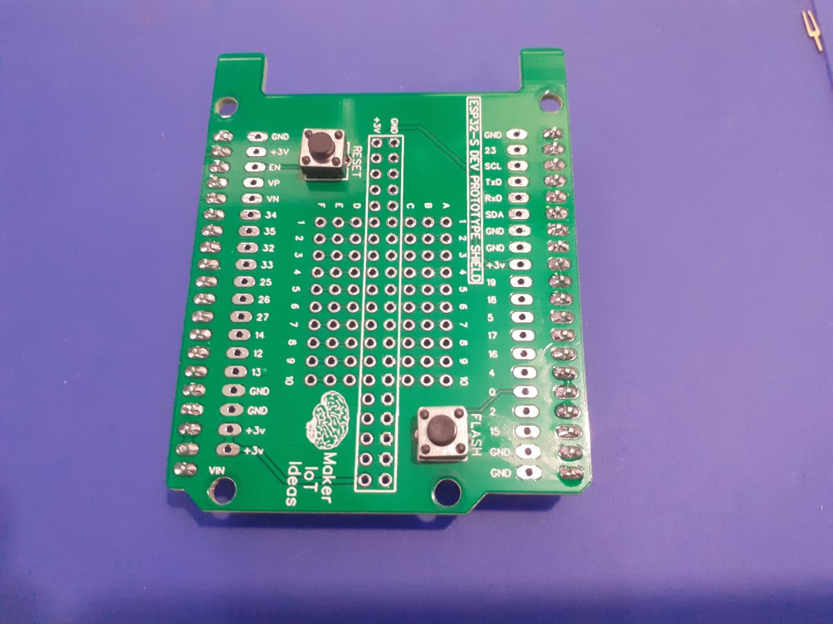
To start off, the PCB is in the same form factor as the ESP32-S Dev Board, namely the Arduino Uno form factor. There are however a few changes, mainly in the number of pins in the headers. This is mainly to accommodate as many of the ESP32-S’s gpio’s as possible. ( Actually, they are all broken out, EXCEPT for the 6 gpio’s that are usually used with the internal Flash memory.)

The PCB is designed to be stacked either on top of, or even below, the ESP32-S Dev Board, depending of course on the type of headers that you decide to solder onto the PCB.

In order to make connecting to the gpio pins easier, each header row is in fact a double row, with solderable pads in parallel for each gpio on the header row.

Flash and Reset buttons are available on top of the shield, they can be fitted of left off, depending on personal preference, as well as how the shield will ultimately be used.

The prototyping area in the centre has been slightly reduced from the standard 5-pin-spacer-5-pin column of the traditional breadboard to a 3-pin-gnd-3v-3-pin column layout. the prototyping holes are at a standard 0.1″ or 2.54mm pitch.

In total, 60 prototype holes, divided into rows of 10, 3 columns deep, are provided, labelled A-F and 1-10.

3.3v and ground are provided in the centre-two rows, to make power easily accessible.

ESP32-S DEV Prototype Shield
ESP32-S DEV Prototype Shield - Back
ESP32-S Dev Prototype Shield – Back

The PCB Design

As this design is basically just two rows of header pins, with a few switches, and a big unconnected prototype area, I did not bother to do a formal schematic for this PCB, but instead jumped straight into the PCB design software and manually designed and routed the tracks and pads that make up this shield.

PCB – Top Layer
PCB – Bottom Layer – Note that this is a “TOP-Down” view, and should be mirrored for actual production

Note that there are big copper pours on both top and bottom layers, in an attemp to reduce electrical noise and provide better shielding.

Manufacturing

The PCB for this project has been manufactured at PCBWay.
Please consider supporting them if you would like your own copy of this PCB, or if you have any PCB of your own that you need to have manufactured.

You can get your own copy here

PCBWay

Some more pictures of the device

Conclusion

Some final thoughts on the completed PCB.
While definitely useful, I have made a purpuseful design flaw on this board, by not including a breakout for the VIN pin. My reasoning at that stage was that I would always be powering the device directly from 3.3v, and would therefor not need access to the VIN pin for power.

Upon completion of the device, and while testing it in a stacked configuration, I realised that that VIN pin would have been quite nice to have access to.

Not a big problem though, as if is very easy to add a 2-pin connector to the power rails, or even solder a wire directly to VIN. Ugly, but totally doable, as this is in fact still a prototype, and it can grow and be fine-tuned to my exact requirements over time.

ESP8266-12E in Arduino Form Factor

As a followup to my recent ESP32-S in Arduino Form Factor device, I decided to also produce a similar circuit board for the ESP8266-12E. Although some people mostly consider these as obsolete, I still find them extremely useful for small projects, and thus use quite a lot of them.

With their lower total pin count and similar low cost to the bigger ESP32 modules, these do force you to get quite creative with the available pins, as well as how and what you can interface.

ESP8266-12E in Arduino Form Factor, with optional I2C pullups as well as Wake from sleep function on GPIO16

What is on the PCB?

For this design, I have once again tried to keep it very lean, including the absolute bare minimum supporting components needed for correct operation.
This includes pull-up and pull-down resistors on the various strapping pins, as well as some decoupling capacitors.

I also did not include a USB-to-Serial converter circuit, as these are used only once or twice, and also consume power while not being needed all the time.
As most of my devices are uploaded OTA anyway, an external stand-alone USB-to-Serial adapter is perfect to upload the initial firmware.

Jumpers to control the onboard I2C pullup-resistors, as well as the Wake-up-from-deep-sleep function on GPIO16 were also added, in addition to the Reset and Flash push-buttons to place the device into initial programming mode.

A 3.3v LDO regulator was also added, for convenience mostly, when powering the device from a bench power supply unit. The recommended voltage for this LDO would in my opinion be 7v Dc, although the datasheet states it can be up to 15v DC… In my opinion, that stresses the component a bit much though, as most of that excessive voltage is dissipated as heat.

PCB Layout – Blank board, front and back

Blank ESP-12E Dev board PCB – Front
ESP-12E Dev board- Back

To try and minimise heat-related issues with the LDO regulator, I have incorporated an on-PCB heatsink for the LDO regulator, which is via-stiched together on both sides of the PCB. This type of heatsink seems to work quite well in many of my other designs, so I decided to use it here as well.

I have also made use of big copper pours on both sides of the PCB to ensure that there is a good ground plane, as well as make use of differential pairs for the routing of the UART and I2C tracks.

Schematic

ESP-12E Dev Board Schematic

PCB Design


Manufacturing

The PCB for this project has been manufactured at PCBWay.
Please consider supporting them if you would like your own copy of this PCB, or if you have any PCB of your own that you need to have manufactured.

You can get your own copy here

PCBWay

Some assembly pictures

Procedure to upload initial firmware

Due to the fact that this device does not have an onboard USB-to-UART (Serial) converter, it will be necessary to use an external device the first time that you upload firmware, or while you are using it on the bench if you do not want to use OTA…

The easiest way to do this, in my opinion, is the following:
1) Power the device from a bench power supply, set at 7V DC via the VIN and GND Pins, available on the bottom left and right of the device ( you can use either side, not both 🙂

2) Now connect your external USB-to-UART converter to the device, as follows:
UART Converter <-> ESP-12E Dev Board
Rx <- TxD
Tx -> RxD
Gnd — GnD

Do Not connect the power (VCC) from the USB-to-UART Converter!

Now start your Adruino IDE, or similar, and connect to the Serial monitor.
Press the reset button on the board, and watch for output in the serial monitor.

If you see output, at 115200 BPS, press end hold flash, and then press and let go of reset, while still holding the flash button.

Wait a few seconds, and then upload your sketch, remembering to manually reset the board after the upload has completed.

I would recommend that you upload the Arduino OTA sketch, from the examples, and modify it to connect to your local WiFi. That way, you will be able to upload all following sketches via your local Wifi, providing that you do not remove the OTA code from the sketch.


ESP32-S in Arduino Form Factor

The ESP32-S is, at least in my opinion, one of the most versatile microcontrollers available to the Maker at this moment. It ticks almost all of my boxes for features required in a microcontroller, with a lot of gpio’s, WiFi, and Bluetooth, as well as a lot of storage space for code.

I do however have an issue with it, which I usually get around by designing a custom circuit board with a specific purpose. This is great for a project, but as most projects do not start on a custom-built circuit board, I am usually required to use a breadboard module. This is where my problems start. These modules are cumbersome to fit on a breadboard, to say the least, taking up a lot of space, and leaving very little space to connect to its pins with anything else.

Some of these modules do not even fit on the breadboard, making it necessary to hang one side off the breadboard or use two breadboards with a gap in the middle. I am quite sure many people can relate to this problem.

My second issue is that when you have done your breadboarding, and want to go to a permanent project, which does not always need a dedicated PCB, you are now required to either live with things on a breadboard, scary to say the least or have a “spider” with many modules and wires, in a box or partly on protoboard etc…

My Solution, the ESP32-S DEV Board, in Arduino Uno form factor

My solution

You can get your own copy here

While not the most elegant, personally I really like the size, and layout of the humble Arduino Uno, with its standardised pinouts, and a large number of addon shields available for the platform. This made me think, sure, there are already ESP32-based boards in this form factor available commercially, but why not make my own instead, as well as a few of my most used modules in a standardised shield form, to make my life just that little bit easier?

The picture above shows my attempt, with most of the GPIO broken out onto female header pins (except for the 6 gpio that are connected to the internal flash chip on the module).

The Blank PCB ( front )
PCB- Back

The PCB explained…

Power:
The board can be powered in two ways, either via the VIN pin ( at an optimal 7.0v DC – the LDO regulator can handle up to 15v, but I personally find that to stress it a bit hard ), which will use the onboard LDO voltage regulator to provide the needed 3.3v or from an external 3.3v PSU, which can provide a bit more current if needed…

There are also plenty of 3.3v and ground connections on the two 20-way headers to connect to other sensors.

Strapping Pins
All the required strapping pins are pulled up or pulled down, as per the datasheet, to 3.3v or ground respectively.

GPIO Pins
All GPIO pins are clearly labelled on the silkscreen to make it easier to use.
I did however not stick to the Arduino labelling convention, as I don’t always use the Arduino IDE, and the actual GPIO numbers are in my view, more useful then.

Flashing code to the board

It will be quite obvious that I did not include any USB-to-serial converter on the board, the reason for this being that, in my opinion,
1) it wastes space on the board
2) it is not actually necessary, as we can upload with an external uart adapter, or use OTA ( which I actually do most of the time )
3) In an actual project, that USB port is going to attract problems, especially if you give it to someone else to use…

A simple Arduino OTA sketch is available in the examples section of the Arduino IDE. It is easy to use and modify and does not need a lot to make it useable with your own sketch…

Antenna Cutout

As recommended by the manufacturer , I have chosen to place the chip inside a cutout on the top of the PCB, with no tracks nearby.

Figure 17: Keepout Zone for ESP32 Module’s Antenna on the Base Board

Although this is not the ideal “best position”, I found that this position worked well with previous designs, and have thus kept it at that.

General comments

As this board is mainly designed for prototype development, I did not bother with dedicated power connectors etc. I did however add proper wide tracks for all the power connections, an on-PCB-heatsink for the voltage regulator, as well as proper ground planes on both sides of the PCB, connected together with via-stitching where needed.

It is also very important to note that this is a 3.3v device. If you need to use sensors or peripherals that operate at other voltages, you will have to use external level converters.

Some assembly pictures

Schematic

Manufacturing

The PCB for this project has been manufactured at PCBWay.
Please consider supporting them if you would like your own copy of this PCB, or if you have any PCB of your own that you need to have manufactured.

You can get your own copy here

PCBWay