ATMEGA4808 with CAN Bus

In This, Part 2 of my CAN Module series( Read Part 1 here), I will look at my recent modification of a previous ATMEGA4808 Development PCB to include CAN bus hardware. The ATMEGA4804 with CAN Bus development board is part of a set of “benchtop development tools” that I designed specifically to design some CAN Bus controlled Gadgets for use in my car…

The PCB is based on a previous project, in which we experimented with alternative chips to replace the ATMEGA328P.

MakerIoT2020 ATMEGA4808 Dev Board

As I was quite happy with the performance of this particular project, I thus decided to use it as the base for the CAN Bus module as well. The Added CAN Hardware adds only a few cm. to the board, keeping it quite compact, although, it will need a complete redesign once I finally get my gadgets finalised 🙂

What is on the PCB ?


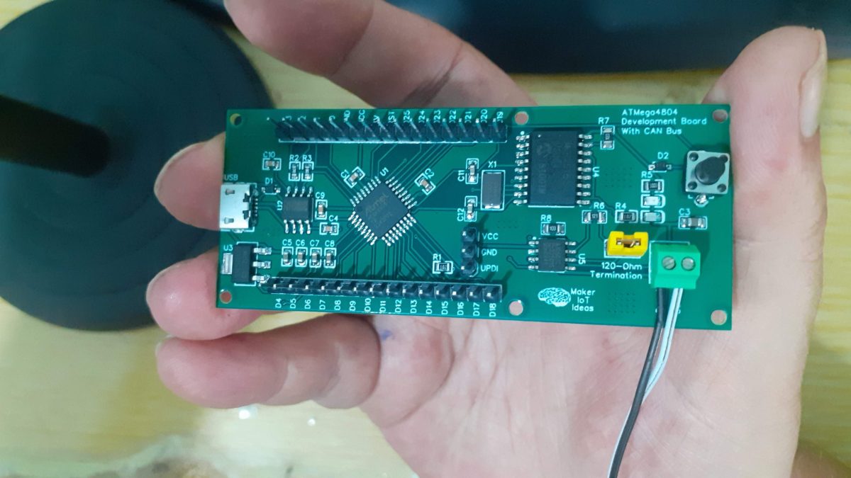
The ATMEGA4808 and its supporting components dominate the left side of the PCB, with a USB connector and a CH340N providing the possibility to upload code to the chip using the Optiboot bootloader. I would however caution you, as there seem to be quite a lot of counterfeit CH340N chips floating around, I received two bad batches already, and from reliable suppliers as well… seems there is something fishy going on in the factory?? Answers anyone?

The Right side of the PCB is dedicated to the CAN Hardware, with the MCP2515 and TJA1050 taking centerstage here. While quite old, the MCP2515 is still readily available for the time being and is also quite affordable. Since I had a few left over from previous projects, I decided to once again make use of what I had on hand.

A 120-Ohm termination resistor ( selectable with a jumper), as well as a screw terminal connector, is provided. The board Reset button, as well as a power and user LED ( on D7), is also in that area of the PCB.

All GPIOs on the ATMEGA4808 were broken out onto header pins, to allow for maximum flexibility and access to features and peripherals on the chip.

Schematic and PCB Design

The Schematic, as mentioned before, is based entirely on a previous project of mine, with the CAN Hardware added onto that. ( I remind everyone once again, that this is a “tool” that I designed for myself to help in getting a specific job done. that will mean that it may or may not be very advanced, or suited for other peoples purposes… but , as a general bench module for CAN Bus development based on the ATMEGA4808, it will be perfect – that is what it was designed to do after all )

Schematic, ATMEGA4808 and supporting components
Schematic, CAN Bus Hardware, MCP2515 and TJA1050

The PCB is a double layer approximately 8.1cm x 3.3cm rectangular module.
6 3.2mm mounting holes are provided.


Manufacturing

I choose PCBWay for my PCB manufacturing. Why? What makes them different from the rest?

PCBWay‘s business goal is to be the most professional PCB manufacturer for prototyping and low-volume production work in the world. With more than a decade in the business, they are committed to meeting the needs of their customers from different industries in terms of quality, delivery, cost-effectiveness and any other demanding requests. As one of the most experienced PCB manufacturers and SMT Assemblers in China, they pride themselves to be our (the Makers) best business partners, as well as good friends in every aspect of our PCB manufacturing needs. They strive to make our R&D work easy and hassle-free.

How do they do that?

PCBWay is NOT a broker. That means that they do all manufacturing and assembly themselves, cutting out all the middlemen, and saving us money.

PCBWay’s online quoting system gives a very detailed and accurate picture of all costs upfront, including components and assembly costs. This saves a lot of time and hassle.

PCBWay gives you one-on-one customer support, that answers you in 5 minutes ( from the Website chat ), or by email within a few hours ( from your personal account manager). Issues are really resolved very quickly, not that there are many anyway, but, as we are all human, it is nice to know that when a gremlin rears its head, you have someone to talk to that will do his/her best to resolve your issue as soon as possible.

Find out more here

Assembly

To save myself time, and ensure that the project is assembled to a high quality standard, I once again opted to have a stencil manufactured in addition to the PCB alone. This is however not strictly required with this board, as the components can still be hand soldered, or solder paste can be manually applied using the method of your choice.

High quality Stainless Stencil
High-quality Stainless Stencil

I used my standard hotplate reflow soldering technique on this board, and it turned out very well indeed, with no solder bridges, making any reworking completely unnecessary, which can in no small part be directly attributed to the super accurate stencil that I used for solder paste application…

Assemble PCB
Assembled PCB

Testing

After assembly, I went through my standard testing ritual, while of course remembering that the ATMEGA4808 is a UPDI programmable chip, which means that you can not just use a USB cable on a brand-new chip…

I uploaded the Optiboot bootloader via that UPDI header, using my own UPDI programmer, that was also a previous project, one that I am very happy to have these days 🙂

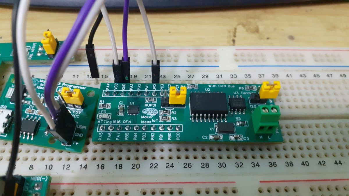
A standard blink sketch followed, and then it was time to test the CAN hardware. For this I used Gary J Fowler’s MCP Can Libray ( the same one that I used with the ATTiny1616 a few days ago ), as well as the ATTiny1616 CAN Module that I build a few days ago…

As for the firmware, at this stage, as I am only concerned about testing actual CAN functionality, I made use of the CAN Loopback on both units, and then THe CAN Sender on the ATTiny1616 and the CAN Receiver on the 4808… These sketches are all available in the library examples… so find them there.

Pinouts for the connections to the MCP2515 from the ATMEGA4808 is as follows:

CS is on Pin D7, MISO on D5, MOSI on D4, SCK on D6 and the Interrupt on D10

The ATTiny1616, which I did not mention in part one, is as follows:
CS on D13,MISO on D15, MOSI on D14, SCK on D16 and the Interrupt on D12

Conclusion

Testing went well, with everything working as expected, with the exception of another batch of CH340N chips being suspect… This does however not really bother me, as I am quite comfortable with using UPDI to upload code, as well as using an external USB-to-serial adapter, connected directly to the UART on the ATMEGA4808.

Cosmetically, I made a labelling error on the silkscreen of the CAN Bus connector, swapping Can H and CAN L… once again, this is not a problem to me.

My thanks to PCBWay for another extremely well-made PCB.

CAN Bus support with the ATTiny1616

ATTiny1616 QFN with Can bus support on a breadboard

A short while ago, I started looking at alternatives to the ATMEGA328P ( the chip used in the standard Arduino Uno). That experiment turned out quite well,
with two of the three chips turning out to be useful, the ATTiny1616 and the Atmega 4808 – The ATTiny 202, while working great, has quite a few severe limitations, due to the size of its memory, as well as library support, limiting its actual useful use quite a bit for my purposes.

In this post, which is part of a two-part series, I will look at adding dedicated CAN Bus support to the 1616 and 8408. I am planning to add some gadgets to my car, and would like to have it controlled by a CAN bus interface, and just maybe, interfacing with the CAN bus on the car as well – at least in the future…

This experiment will thus consist of two prototypes with onboard CAN hardware, to be initially used on the bench while building and testing my gadgets – more on them later, if and when they work out the way that I imagine.

What is on the PCB

The ATTiny1616 microcontroller, in a QFN package, has been married to a MCP2515 and a TJA1050. These chips, while old, are still easy to get hold of,
and I have quite a few of them lying around from previous projects. It did thus seem to be a good starting point. The fact that their libraries also works perfectly with the ATTiny1616 and Atmega4808 also went a long way towards selecting them for the project.

The PCB is similar to the ATTiny1616 QFN breakout that I have designed before but with the addition of the CAN-related components.

ATTiny1616 QFN development board with CAN bus, after reflow soldering

Schematic and PCB Design

The schematic is a variation on the earlier breakout PBC, with the addition of the CAN-related components.

ATTiny1616 Schematic - MCU only,
Can bus related components - for use thie the ATTiny1616 MCU


The PCB design has also not changed a lot, I have just added the CAN components to the right hand side of the PCB, and adjusted the routing.

PCB layout design for the ATMEGA1616 with CAN bus Development PCB


3D render of the PCB, with the header pins in non-breadboard configuration – with the CAN bus connector not fitted.

Manufacturing

I choose PCBWay for my PCB manufacturing. Why? What makes them different from the rest?

PCBWay‘s business goal is to be the most professional PCB manufacturer for prototyping and low-volume production work in the world. With more than a decade in the business, they are committed to meeting the needs of their customers from different industries in terms of quality, delivery, cost-effectiveness and any other demanding requests. As one of the most experienced PCB manufacturers and SMT Assemblers in China, they pride themselves to be our (the Makers) best business partners, as well as good friends in every aspect of our PCB manufacturing needs. They strive to make our R&D work easy and hassle-free.

How do they do that?

PCBWay is NOT a broker. That means that they do all manufacturing and assembly themselves, cutting out all the middlemen, and saving us money.

PCBWay’s online quoting system gives a very detailed and accurate picture of all costs upfront, including components and assembly costs. This saves a lot of time and hassle.

PCBWay gives you one-on-one customer support, that answers you in 5 minutes ( from the Website chat ), or by email within a few hours ( from your personal account manager). Issues are really resolved very quickly, not that there are many anyway, but, as we are all human, it is nice to know that when a gremlin rears its head, you have someone to talk to that will do his/her best to resolve your issue as soon as possible.

Find out more here

Assembly

I usually can not wait to receive my creations back from the factory – I mean, how can somebody not get excited about receiving their own PCBs back from the factory, especially if you know they will be of the high quality that I have come to trust with all of my PCBWay orders?

This is especially true of the smaller PCBs, as well as those with smaller-sized QFN components, with this board definitely not being an exception.

ATTiny1616 QFN Dev board with Can Bus, in packaging - straight from the factory
PCBs in factory packaging
PCBs in protective wrapping, after opening
PCBs in protective wrapping, just after opening the package
Closeup view of the top side of the PCB

This PCB once again requires the use of a stencil, to accurately apply just the right amount of solder paste to the pads, especially the small QFN package pads of the ATTiny 1616…

High quality stainless steel, laser cut stencil. High accuracy. Definitely worth the investment
High-quality stainless steel, laser cut stencil.

Stencils, at least from my point of view, can be a controversial subject, with some hobbyists arguing that they are not worth the additional expense… I do however believe that they actually save you a lot, in time that you don’t waste on reworking a PCB due to solder bridges, in the correct amount of solder paste that is applied, in the correct thickness, and also time not wasted on the cleanup of the mess that can result from manually applying solder paste.

After solder paste application, all the components are placed in their correct positions, ready to be reflow soldered.
PCB ready for reflow soldering, after manually placing the components in their respective places

The PCB is now reflow soldered with a hot plate, and allowed to slowly cool down afterwards, to reduce thermal shock damage to the joints, that may result from a too-quick cooldown cycle. While I do not own a dedicated reflow oven, the hotplate that I use, seems to match the reflow profile ramp-up of my solder paste, and most of the components perfectly. After achieving a complete solder melt, at about 223 degrees C, I usually switch of the hot plate, and carefully move the PCB towards the edge of the unit, that area is usually a bit cooler than the centre. leaving it there for about 5 to 8 minutes, allow the solder to slowly solidify, after which I remove it and place it on a silicone mat to cool completely.

Through-hole component soldering, and testing

The next step is soldering all the through-hole components, usually header pins and connectors into their respective places. The board is then placed onto a solderless breadboard, and various test sketches are uploaded via a homemade UPDI programmer.

These include the infamous blink sketch, to make sure the chip is alive and survived the reflow soldering. That is followed by a CAN loopback test, and then the actual CAN firmware… I make use of the excellent MCP Can library from Garry J Fowler, as well as the megaTinyCore Arduino core, from Spence Konde.

My thanks to both of these gentlemen, for their excellent and easy-to-use software. A special shoutout to Garry J Fowler, since his MCP Can library correctly releases the CE pin of the device when not in use, thus not locking up the spi bus. [ This is something that many other libraries do not bother to care about ] …

Conclusion

This was once again a fun project to design and assemble. The real testing and development can now start at full speed, as this is just meant to be a tool, with a further revision later down the line. It does of course help a whole lot that I can completely trust my PCB manufacturer, PCBWay, to deliver my PCBs to me EXACTLY as I designed them, and at extremely high quality and precision! Thank you for that!

Stereo I2S Shield – The next iteration…

Last month I started working on a Stereo I2S Audio shield for my ESP32-S development board. Those of you that saw that post will remember that I made some mistakes on the initial prototype, and had to repair it with a few “greenwire” connections.


The prototype shield also required the use of commercial I2S modules to be plugged into it, making for quite a cumbersome first iteration.

Stereo I2S shield stacked onto esp32-S dev board

I decided to do something about that, as the long-term use of this particular shield, as internet radio, with a further “dream” of using it as a remote media player for use from Home Assistant, is moving along well, with progress on the firmware being made slowly but surely.


I decided that, since the Audio Chips seem to be quite easily available, and are modestly priced, getting rid of the plug-in modules, and placing the chips directly on the shield seemed like the next logical step. I also broke out the gain pins of each chip and made provision for easily changing said gain with a jumper, individually for the left and right channels of the I2S Audio shield.

I decided to keep the logic level conversion circuit, as it worked well, as well as provided another layer of protection to the ESP32-S that drives the whole shield. ( These have recently been discontinued by AI-Thinker, but the Espressif version is still begin manufactured and supported).

The power supply section of the board remains the same as the previous version, with a dedicated 5v regulator feeding the Audio section, and a 3v regulator the logic level converters. (I may change this in future, as the ESP32-S board can easily supply the 3v required without overloading the regulator on the CPU board.

Current issues that are carried over from the initial prototype still remain though. The two I2S Audion chips seem to be QUITE power-hungry, pulling almost 2A of current from a 12v supply, with a modest volume of 10 out of a possible 100. This has been reduced down from an earlier 4A to 6A when using a different pair of 4ohm 3W speakers.

This is also one of the reasons for the separate voltage regulators on the shield.

Manufacturing

I choose PCBWay for my PCB manufacturing. Why? What makes them different from the rest?

PCBWay‘s business goal is to be the most professional PCB manufacturer for prototyping and low-volume production work in the world. With more than a decade in the business, they are committed to meeting the needs of their customers from different industries in terms of quality, delivery, cost-effectiveness and any other demanding requests. As one of the most experienced PCB manufacturers and SMT Assemblers in China, they pride themselves to be our (the Makers) best business partners, as well as good friends in every aspect of our PCB manufacturing needs. They strive to make our R&D work easy and hassle-free.

How do they do that?

PCBWay is NOT a broker. That means that they do all manufacturing and assembly themselves, cutting out all the middlemen, and saving us money.

PCBWay’s online quoting system gives a very detailed and accurate picture of all costs upfront, including components and assembly costs. This saves a lot of time and hassle.

PCBWay gives you one-on-one customer support, that answers you in 5 minutes ( from the Website chat ), or by email within a few hours ( from your personal account manager). Issues are really resolved very quickly, not that there are many anyway, but, as we are all human, it is nice to know that when a gremlin rears its head, you have someone to talk to that will do his/her best to resolve your issue as soon as possible.

Find out more here

Assembly

This project once again called for a stencil, as the QFN packages of the Audio chips are super tiny, with super tiny tracks and pads. A high-quality stencil definitely goes a long way in ensuring that just the right amount of solder paste is added to each pad. This also reduces the requirements for reworking a board with hot air to fix any solder bridges that might have formed.


The quality of a stencil says a lot about your PCB manufacturer, and in my case, I am extremely happy to say that PCBWay definitely delivers quality. Having used their services for close to 3 years now, I have not received a single faulty PCB or stencil at all. Yes, some PCB’s has had errors, but those were all MY errors. Design errors, not manufacturing errors.

Let us return to the assembly of this PCB, shall we…

As usual, the PCBs arrived very well packaged, and after a quick inspection and some random tests with a multimeter, It was time for solder paste and placing components, while listening to a piece of relaxing music… my way of relaxing…


After about 20 minutes of intense concentration, we have a PCB with all of the components correctly placed onto their respective pads, ready for reflow soldering.


I did things differently this time, by placing the QFN Audio chips in their positions at the same time as all the others. ( I usually drop them in place when the solder is in a liquid state, but with these, I was confident in the stencil, and as these chips were quite a bit more expensive than my usual projects [ over 3 USD each ], I wanted them to slowly get up to temperature, and spend as little time as possible at temperature as well. )


Reflowing was a success, and after inspection, no solder bridges were found. A detailed diagnostic with a multimeter with fine-tipped needle probes confirmed that there were no short circuits or bridges, and I could thus continue with the rest of the assembly – the various through-hole components, being mostly header pins, switches and a DC barrel jack socket.

The speaker wires were soldered directly to the PCB, due to the fact that being a prototype, I did not see the need to raise the cost even more by adding connectors onto a board that may not be used very long if it turns out that there is a problem somewhere.

Testing

The next stage was testing, using the software provided in the initial Stereo I2S Shield post. All went well, but, as mentioned above, I encountered the same high current draw issue, which resolved itself ( in a manner of speaking ) after I reduced the initial startup volume of the unit, and limited the maximum volume in the software.

I can now continue with firmware development, and sort out things like the rotary encoders for the volume and station selection, as well as look at adding an i2c display, and possibly a sd-card for stored music files.

Conclusion

The project is getting along quite well, and this iteration of the prototype did not have any design faults or errors. I am extremely impressed with the reliability of my PCB manufacturer, as their consistent quality products allow me to focus on design, and trust that whatever comes back from the factory will be exactly as I designed it.

While there are still quite a few issues to sort out on this project, I am confident that in the end, it will all turn out the way that I want it to.

My Own DC-DC Buck Converter

Dc-to-DC Back converters have a lot of advantages over traditional linear voltage regulator solutions. Most of these advantages are related to the smaller size of these circuits, in comparison to their linear counterparts, as well as their higher efficiency and lower power consumption to name a few.

I am by no means a power supply guy, and as such, I usually buy my power supply modules. The same also applies to boost and buck converters. I am usually quite comfortable leaving the design of these critical parts to those who actually know what they are doing.

It thus seemed like a reasonable challenge to actually try and design and build one by myself, and that will be the story behind this post.

Finding a suitable driver IC

This journey started at a very strange place. When I decided to go ahead and build this Buck converter module, I had no specific driver IC in mind. I was thus browsing through the long list of dc-to-dc- buck converters on my component suppliers’ website, randomly pulling up a datasheet to take a closer look, mainly looking for something with as few external components as possible, while also having a decent current supply capability, as well as being able to operate on an input supply of 4v to about 24v, which is well within my usual range…

I eventually settled on the MPS MP9943. Definitely not the cheapest but still affordable, and in a QFN8 package, so that I am still able to actually solder it to a PCB!

-Wide 4V to 36V Continuous Operating Input
Range
-85mΩ/55mΩ Low RDS(ON) Internal Power
MOSFETs
-High-Efficiency Synchronous Mode Operation
-410kHz Switching Frequency
-Synchronizes from 200kHz to 2.2MHz
-External Clock
-High Duty Cycle for Automotive Cold-crank
-Internal Power-Save Mode
-Internal Soft-Start
-Power Good Indicator
-Over Current Protection and Hiccup
-Thermal Shutdown
-Output Adjustable from 0.8V
-Available in an QFN-8 (3mmx3mm)
package

and with a peak current supply of up to 3A – Not too bad at all.

The actual design

As mentioned already, I am not ( or at least I don’t see myself) a power supply design expert. I believe I am perfectly capable with the linear stuff, by switchmode was never my strong point 🙂 This prototype will just be based on the recommended design in the datasheet, at least for the first version, and then, later versions may feature some customisation as actually needed.

From the picture above, we can see that there are indeed not a lot of external components required. And in my humble opinion, the efficiency vs load also seems to be quite reasonable.

I thus went ahead and started reading this datasheet in detail. I found two typical-use circuits with recommended component values, from which I build my prototype.

I chose to combine these two circuits to give me a variable output module, that will be selectable between 5v and 3v.

I also chose an inductor with a 6A maximum current rating, as the datasheet states that we should choose one with at least a 25% higher current rating than our peak requirement. My logic here was that 100% would be a good number, as the inductor would in theory never saturate?? as well as produce less heat etc ?? Please comment on this, as I may be barking up the wrong tree here 🙂


The schematic above is what I came up with. A jumper will allow the selection of the output voltage, as this is determined by the value of the resistor at R8, in my case 13K or 7.68k… I also assume that that resistor can later be replaced by a 20k trimpot or similar to give a truly variable output.

PCB Layout

The PCB layout was an attempt to follow the datasheet recommendations as closely as possible, while still having my own design. I am also aware that I may have wasted quite a bit of space, but for now, my focus is on getting a working design. I can always try to squeeze it into a smaller space later.

Manufacturing

I choose PCBWay for my PCB manufacturing. Why? What makes them different from the rest?

PCBWay‘s business goal is to be the most professional PCB manufacturer for prototyping and low-volume production work in the world. With more than a decade in the business, they are committed to meeting the needs of their customers from different industries in terms of quality, delivery, cost-effectiveness and any other demanding requests. As one of the most experienced PCB manufacturers and SMT Assemblers in China, they pride themselves to be our (the Makers) best business partners, as well as good friends in every aspect of our PCB manufacturing needs. They strive to make our R&D work easy and hassle-free.

How do they do that?

PCBWay is NOT a broker. That means that they do all manufacturing and assembly themselves, cutting out all the middlemen, and saving us money.

PCBWay’s online quoting system gives a very detailed and accurate picture of all costs upfront, including components and assembly costs. This saves a lot of time and hassle.

PCBWay gives you one-on-one customer support, that answers you in 5 minutes ( from the Website chat ), or by email within a few hours ( from your personal account manager). Issues are really resolved very quickly, not that there are many anyway, but, as we are all human, it is nice to know that when a gremlin rears its head, you have someone to talk to that will do his/her best to resolve your issue as soon as possible.

Find out more here

Assembly

After receiving the PCBs back from the factory, and receiving the components from the supplier, I started on the assembly. While uneventful, It was worth mentioning that this project does require a stencil. The DFN-8 package is quite small (only 3mmx3mm), with eight leads, so that makes for some tiny spacing between them. As it is also a leadless package, I did not want to chance to have too much solder paste in there.

As we can clearly see in the picture above, the pads are super tiny. The other components are 0805 ( for reference).

My standard way for assembling DFN packages is to actually level the part of the PCB while reflowing the PCB with a hotplate. Then, when the solder has all melted and is in a liquid state, I carefully place the part with tweezers and remove the PCB from the hotplate.

Alternatively, I remove the PCB from the hotplate first, leaving it to cool down a bit, and then, using a hot air gun with a small nozzle, reflowing only the area where the part needs to be placed, and carefully placing it onto the melted solder.

Both of these methods seem to be working quite well, for me at least, but the hot air method does however have the risk of a bit of solder splatter, which may form unwanted bridges… The part also gets heated a bit, as it has to be held in place for a few seconds to prevent it from being blown around by the hot air.

Testing


I am quite happy to report that the module works as expected, with a steady output of 3.31v and 5.08v respectively at no load.

Under load, I tested with a 1A and 2A load respectively, both voltages are also stable. Ripple, as measured by myself, and using a “not too good” digital oscilloscope, seems to be about 110mv peak-to-peak.

Using better probes, and a better scope, I may be able to get a better and more accurate reading.

Conclusion

This was quite an exciting project, with setting myself a challenge, and actually achieving what I set out to do. While I am sure that the module in its current state may actually not quite be perfect, and that it surely has a lot of room for improvement, I am satisfied with its performance, and just plainly, the fact that it actually works!