Battery Backup for your Pi Zero (W) is a very important feature to prolong the life of the SD Card. Many commercially available solutions exist, in the form of Hats, but, unfortunately, it seems that anything that was specifically designed for the Raspberry Pi, can be quite expensive.
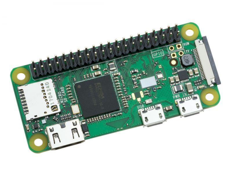
The 40 pin header on our Raspberry Pi Zero / Zero W gives us a lot of potentials to expand the functionality of this tiny single-board computer, but it, unfortunately, suffers from two major flaws, from my point of view of course.
- The pins are scattered all over the place, and not grouped by function.
Access to the pins is also very cluttered, to keep the overall footprint of the board small. - The GPIO pins are 3v only; adding anything that runs on a different voltage becomes a messy
assembly of wires and level converters and or resistor dividers… going to a breadboard…

My Solution
Solving these issues required a lot of deep thinking, it actually took me a few months, during which I looked at various commercial solutions, imagined things in my mind, as well as tested concepts and various modules.
Let us take a look at some of these before I show you the solution that I am currently working on.
Battery Power
I would like to use a single 18650 LiPo cell to power the Pi Zero. Other Battery Backup solutions make use of this as well. In the ideal world, a pair of these in parallel would be great. The 18650 cell is a 3.3 volt ( nominal 4.2v) LiPo cell. The Pi needs 5v to run. This would require a Boost converter, as well as a dedicated LiPo charging circuit to recharge the cell after use.
Many such charging and Boost converters are available, but they seem to suffer from a problem, they need a dedicated charging cycle, during which using the device is not advised.
I could design my own circuit, but as I do not consider myself a proficient power supply designer, and with the huge amount of professionally designed, low-cost modules available, I decided to use the MH CD-42 module instead.


This module seems to give me all the features I need, with only one exception: The input voltage MUST be between 5.0v and 5.5v. I hope to address that issue later though.
It can source up to 2A at 5v, and most importantly, has a current bypass function, which allows you to charge the battery, as well as power an external device at the same time.
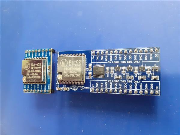
GPIO Pin Grouping and Level Conversion
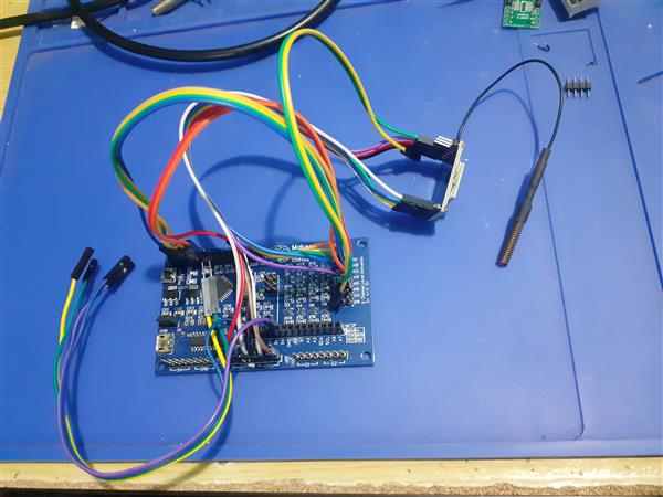
The next logical step was to design a base-board that contained the 18650 Cell, and power module, as well as provide access to the GPIO pins.

I decided to use a 90 degree 2×20 pin Female header to mount the Pi, allowing for plenty of airflow around it to prevent overheating, as well as clearly labelled header pins for access to the GPIO pins.
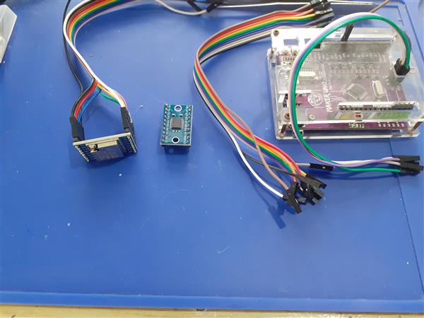
( Due to logistics issues, the female header pin has not arrived yet).
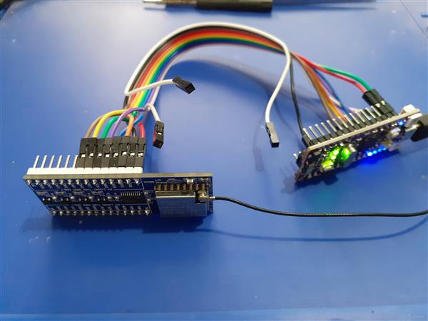
The logic level conversion was provided on some of the GPIO ( SPI0, SPI1, I2C and UART ) by using the TXS0108E 8Ch Bidirectional Level Shifter chip from TI. Headers in black are 3v ( with exception of GPIO13) and 5v logic pins are on a white header.
Additional Ground and Power headers for 5v and 3v (red headers) were also added.
Finally, a dedicated shutdown button was connected to GPIO26.
Schematic

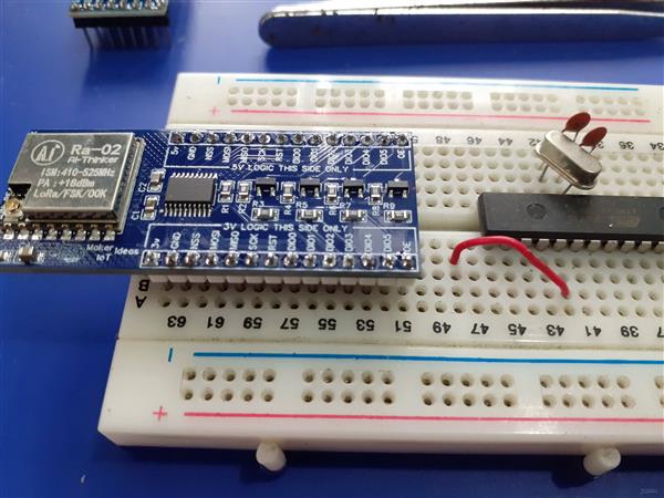
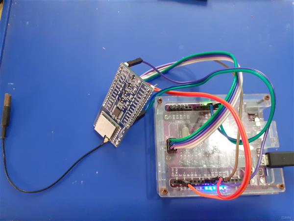
Testing the prototype
The prototype is still under testing, as mentioned above, I still have to receive the 40 pin female header.
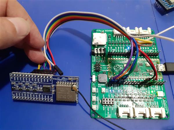
I did however connect the Pi Zero to the board with jumper wires ( 3v, 5v and ground only ) to test operation. So far, the setup provides 5 hours of battery backup with the Pi on idle, no external devices connected and running only an MQTT server on Raspberry Pi Lite OS ( No Gui )

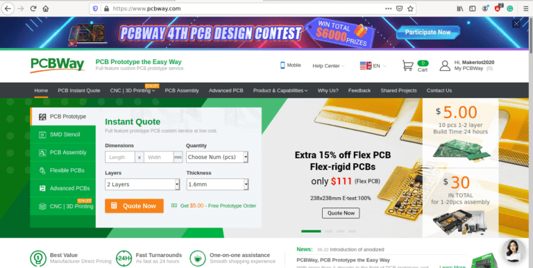
The first revision of the device is available for order at PCBWay
Manufacturing the PCB

This PCB was manufactured at PCBWAY. The Gerber files and BOM, as well as all the schematics, will soon be available as a shared project on their website. If you would like to have PCBWAY manufacture one of your own, designs, or even this particular PCB, you need to do the following…
1) Click on this link
2) Create an account if you have not already got one of your own.
If you use the link above, you will also instantly receive a $5USD coupon, which you can use on your first or any other order later. (Disclaimer: I will earn a small referral fee from PCBWay. This referral fee will not affect the cost of your order, nor will you pay any part thereof.)
3) Once you have gone to their website, and created an account, or login with your existing account,
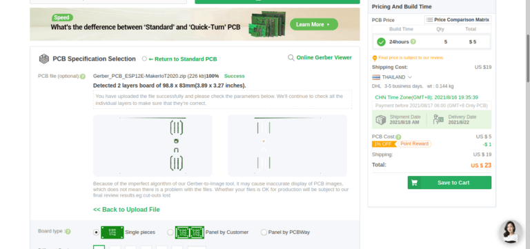
4) Click on PCB Instant Quote

5) If you do not have any very special requirements for your PCB, click on Quick-order PCB

6) Click on Add Gerber File, and select your Gerber file(s) from your computer. Most of your PCB details will now be automatically selected, leaving you to only select the solder mask and silk-screen colour, as well as to remove the order number or not. You can of course fine-tune everything exactly as you want as well.

7) You can also select whether you want an SMD stencil, or have the board assembled after manufacturing. Please note that the assembly service, as well as the cost of your components, ARE NOT included in the initial quoted price. ( The quote will update depending on what options you select ).
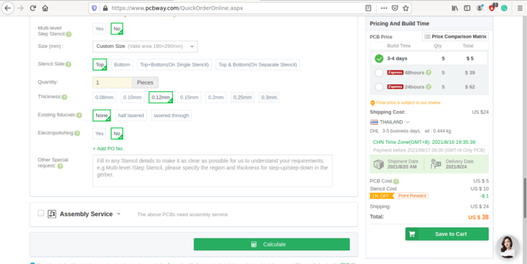
8) When you are happy with the options that you have selected, you can click on the Save to Cart Button. From here on, you can go to the top of the screen, click on Cart, make any payment(s) or use any coupons that you have in your account.
Then just sit back and wait for your new PCB to be delivered to your door via the shipping company that you have selected during checkout.