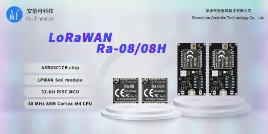
The Ai-Thinker company in Shenzen has recently introduced two new LoRa radio modules, the Ra-08 and Ra-08H. These new LoRaWAN modules are based on the ASR Microelectronics ASR6601 module featuring a 48MHz ARM Cortex M4 microcontroller and Semtech SX1262 transceiver allowing long-range, low power communication for the Internet of Things.
Both LoRaWAN modules share most of the same specifications, but the Ra-08 module operates in the 410-525MHz frequency band, while the Ra-08H module works in the widely used 803MHz to 930MHz band. Ai-Thinker also provides a development kit for each module.
Ai-Thinker Ra-08/Rs-08H key features and specifications:
Programmable embedded Arm Cortex-M4 MCU with 128 KB of Flash and 16 KB of SRAM
Power Consumption – Down to 0.9uA in deep sleep mode
Dimensions – 16 x 16 x 3.2m (SMD-18 package)
The modules support OTA firmware updates, and the company also provides PDF documentation for the individual modules, as well as Ra-08-kit and Ra-08H-kit development kits. Most of the documents are however still in Chinese, but can easily be translated with Google translate to make them easily understandable.
The modules feature a factory-installed AT-Command set for rapid application development, as well as the capability to completely reprogram the ARS6601 with your own custom firmware, using STMCube IDE from ST Microelectronics. At the moment, there does not seem to be any STMDuino support available for these, but we are sure that will change in the near future, as they gain popularity with users.
Applications
The Ra-08/08H modules, and ASR6601 LoRaWAN chip, enable a new generation of indoor and outdoor IoT applications such as smart agriculture, smart cities, smart meters, asset tracking, streetlights, parking sensors, smoke sensors, smart environmental monitoring, automation in the smart home, building automation, and more.
If you’d like to find out more, or order samples, please check out the Ai-Thinker website or contact them by email at overseas@aithinker.com.
Special Offer MakerIoT2020 has two sets of Ra-08 and RA-08H development kits available for two lucky readers, limited to one set each. These modules are unused and brand new from the factory. Find out more on our Facebook and Instagram pages on how to stand a chance to get them for free (shipping to your own account)
In part one of this series, I took a look at some of my experiments using different voltage regulators, to design and build the Remote Alarm Transceiver prototype, and also mentioned that I will be looking at a single chip logic converter solution. In this (hopefully short) post, I will take a detailed look at that logic converter chip, as well as show you how it is used.
Some of the features of the device is listed below:
• AEC-Q100 Qualified for Automotive Applications – Device Temperature Grade 1: –40°C to 125°C – Device HBM ESD Classification Level 2 – Device CDM ESD Classification Level C6 • No direction-control signal needed • Maximum data rates – 110 Mbps (push pull) – 1.2 Mbps (open drain) • 1.4 V to 3.6 V on A port and 1.65 V to 5.5 V on B port (VCCA ≤ VCCB) • No power-supply sequencing required – either VCCA or VCCB can be ramped first • Latch-up performance exceeds 100 mA per JESD 78, Class II • ESD protection exceeds JESD 22 (A Port) – 2000-V human body model (A114-B) – 1000-V charged-device model (C101) • IEC 61000-4-2 ESD (B port) – ±8 kV contact discharge – ±6 kV Air-gap discharge
Datasheet description:
This device is an 8-bit non-inverting level translator that uses two separate configurable power-supply rails. The A port tracks the VCCA pin supply voltage. The VCCA pin accepts any supply voltage between 1.4 V and 3.6 V. The B port tracks the VCCB pin supply voltage. The VCCB pin accepts any supply voltage between 1.65 V and 5.5 V. Two input supply pins allows for low Voltage bidirectional translation between any of the 1.5 V, 1.8 V, 2.5 V, 3.3 V, and 5 V voltage nodes. When the output-enable (OE) input is low, all outputs are placed in the high-impedance (Hi-Z) state. To ensure the Hi-Z state during power-up or power-down periods, tie OE to GND through a pull-down resistor. The minimum value of the resistor is determined by the current-sourcing capability of the driver.
Typical Application:
Reference Design / Typical Application for the TXS0108E
My Thoughts:
I really like the tri-state (high impedance) mode of the chip, as it allows for isolation between the different voltage level circuits, for example, If I were to communicate on a 5v SPI bus, to another device, I can for instance put the chip in Tri-state mode, and not worry about stray signals interfering from the 3v side.
On the downside, the chip is very small, which makes it a real challenge to solder by hand. On the speed side, It is also not quite as fast as my usual MOSFET based circuitry. It does however do the job it was designed for quite well.
Updated Circuit
Integrating the chip into the existing Remote Alarm Transceiver circuit is very easy, allowing us to replace almost all of the Mosfet-based Logic level converters. We do still need a few of them, as we have only 8 bidirectional channels on the TXS0108.
Schematics
Some Notes on the schematics:
A battery level monitor is connected through a voltage divider, with a MOSFET as a switch to the A0 pin. The voltage divider is set up for a 12v DC input source. The MOSFET is controlled from the D6 Pin.
The reason that I did this is, that I found some parasitic voltage leakage through the A2D converter in a previous design, reducing battery life. My hope is that by only reading battery level when the MOSFET is on, there can be an increase in battery life ( Taking into consideration that the Voltage regulators are not very efficient, it won’t really amount to a big gain unless I switch to an SMPS in the future. )
The PCB
The PCB
In the picture above, we can see the completed PCB (The relay and buzzer were not populated yet)
Manufacturing the PCB
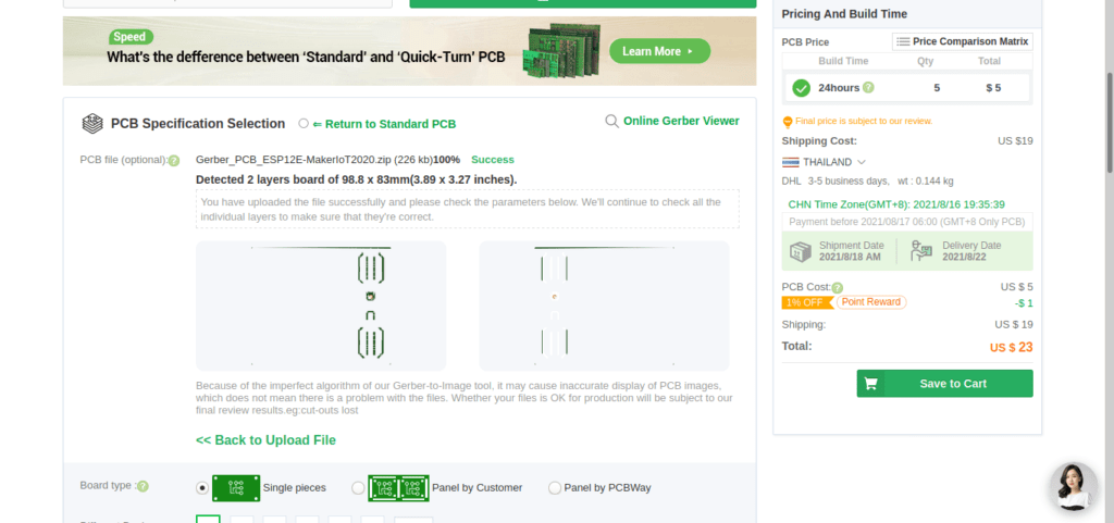
This PCB was manufactured at PCBWAY. The Gerber files and BOM, as well as all the schematics, will soon be available as a shared project on their website. If you would like to have PCBWAY manufacture one of your own, designs, or even this particular PCB, you need to do the following… 1) Click on this link 2) Create an account if you have not already got one of your own. If you use the link above, you will also instantly receive a $5USD coupon, which you can use on your first or any other order later. (Disclaimer: I will earn a small referral fee from PCBWay. This referral fee will not affect the cost of your order, nor will you pay any part thereof.) 3) Once you have gone to their website, and created an account, or login with your existing account,
4) Click on PCB Instant Quote
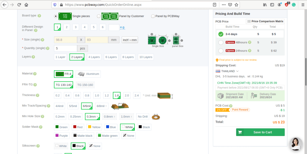
5) If you do not have any very special requirements for your PCB, click on Quick-order PCB
6) Click on Add Gerber File, and select your Gerber file(s) from your computer. Most of your PCB details will now be automatically selected, leaving you to only select the solder mask and silk-screen colour, as well as to remove the order number or not. You can of course fine-tune everything exactly as you want as well.
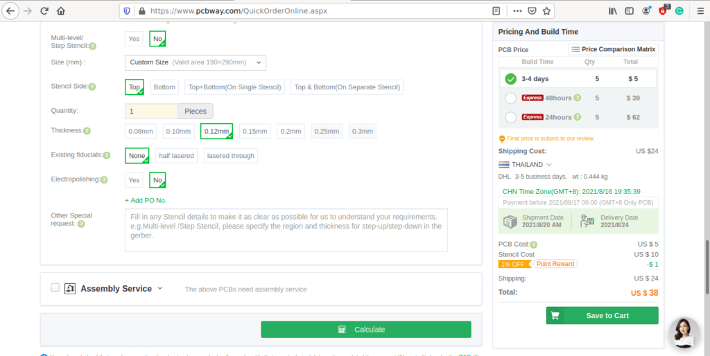
7) You can also select whether you want an SMD stencil, or have the board assembled after manufacturing. Please note that the assembly service, as well as the cost of your components, ARE NOT included in the initial quoted price. ( The quote will update depending on what options you select ).
8) When you are happy with the options that you have selected, you can click on the Save to Cart Button. From here on, you can go to the top of the screen, click on Cart, make any payment(s) or use any coupons that you have in your account.
Then just sit back and wait for your new PCB to be delivered to your door via the shipping company that you have selected during checkout.
As part of my experiments with LoRa and the easy to use ATMega328P, I have recently designed quite a few LoRa based projects. In this final 2 part series, I will look at two additional projects, part of a Remote Alarm Transceiver, where I experimented with a changing a few things:
– Using LM317G adjustable voltage regulators. – Replacing my standard N-MOS based logic level converters with a dedicated chip.
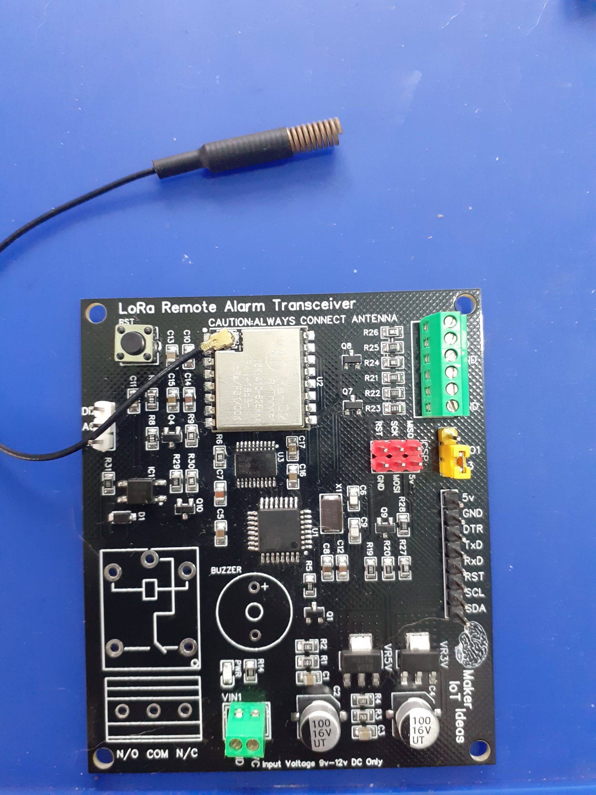
LoRa Remote Alarm Transmitter – with Onboard Relay putout and two sensor inputs
How does this differ from my other LoRa Based projects?
The PCB presented above does in fact not really differ a lot from any of my existing LoRa based projects. However, there are a few subtle changes, mainly experimental changes, brought on by factors such as component availability and an attempt to reduce component counts and board size.
The first of these changes is using the LM317G voltage regulator, in the place of my usual LM1117 3.3 and 5.0 LDO regulators.
The LM317 is an old device, It has been on the market for a long time. It can supply up to 1.5A of current, and a single device can be configured to supply a wide range of different voltages by just changing two resistors. This seemed quite attractive to me, as it is getting quite difficult to reliably get quite a few components on time, and with decent pricing in the post-Covid-19 world.
The second major change would be moving away from my existing N-Mos based Logic converter setup, where I used the BSS138 and 10K resistors as logic converters. This setup works perfectly, but it has the drawback of requiring quite a lot of components. for example:
To provide logic conversion to an RA-02 module, with access to all the IO Lines (GPIO0-5 included) required 12 BSS138 Mosfets and 24 10k resistors. This is quite a lot of components. A dedicated logic converter chip would thus be a much more attractive solution.
Driver circuitry for sensor Inputs, consisting of a simple transistor input, and an optically isolated Relay output completes the circuit.
Using the LM317
The output voltage of the LM317 is typically set using two resistors, with a suitable current rating, using the following Formula
VOUT = 1.25 * ( 1 + R2/R1 )
It is also common to use a variable resistor at R2, to have fine control over the output voltage. This is due to the fact that stock resistor values do not always give you the exact voltage you require. You should also take into account that using a 5% resistor will be less accurate than a 1% resistor.
The grid below is a list of common stock resistor values for R1/R2, with the resulting voltage produced.
R1 vs R2 Grid for use in selecting fixed output voltage
R2\R1
150
180
220
240
270
330
370
390
470
68
1.82
1.72
1.64
1.60
1.56
1.51
1.48
1.47
1.43
82
1.93
1.82
1.72
1.68
1.63
1.56
1.53
1.51
1.47
100
2.08
1.94
1.82
1.77
1.71
1.63
1.59
1.57
1.52
120
2.25
2.08
1.93
1.88
1.81
1.70
1.66
1.63
1.57
150
2.50
2.29
2.10
2.03
1.94
1.82
1.76
1.73
1.65
180
2.75
2.50
2.27
2.19
2.08
1.93
1.86
1.83
1.73
220
3.08
2.78
2.50
2.40
2.27
2.08
1.99
1.96
1.84
240
3.25
2.92
2.61
2.50
2.36
2.16
2.06
2.02
1.89
270
3.50
3.13
2.78
2.66
2.50
2.27
2.16
2.12
1.97
330
4.00
3.54
3.13
2.97
2.78
2.50
2.36
2.31
2.13
370
4.33
3.82
3.35
3.18
2.96
2.65
2.50
2.44
2.23
390
4.50
3.96
3.47
3.28
3.06
2.73
2.57
2.50
2.29
470
5.17
4.51
3.92
3.70
3.43
3.03
2.84
2.76
2.50
560
5.92
5.14
4.43
4.17
3.84
3.37
3.14
3.04
2.74
680
6.92
5.97
5.11
4.79
4.40
3.83
3.55
3.43
3.06
820
8.08
6.94
5.91
5.52
5.05
4.36
4.02
3.88
3.43
1000
9.58
8.19
6.93
6.46
5.88
5.04
4.63
4.46
3.91
1200
11.25
9.58
8.07
7.50
6.81
5.80
5.30
5.10
4.44
1500
13.75
11.67
9.77
9.06
8.19
6.93
6.32
6.06
5.24
1800
16.25
13.75
11.48
10.63
9.58
8.07
7.33
7.02
6.04
2200
19.58
16.53
13.75
12.71
11.44
9.58
8.68
8.30
7.10
2700
23.75
20.00
16.59
15.31
13.75
11.48
10.37
9.90
8.43
3300
28.75
24.17
20.00
18.44
16.53
13.75
12.40
11.83
10.03
As you can see from the table above, using stock resistors, the output voltage is reasonably accurate, but it is quite obvious that you will need a potentiometer to get exact values. Another issue will definitely be heat dissipation. In my PCB design, I have used the SOT-223 package of the component, with a PCB heatsink, built directly into the layers. With the LM1117 LDO regulators, these work extremely well.
Logic Level Conversion
In this design, I used my standard Logic Level conversion circuit, comprised of a BSS138 N-Mos with two 10 k resistors. This circuit, although a bit cumbersome with lots of components if you need many logic converters, is very stable, and functions extremely well.
Conclusion
This circuit was designed as a two-part prototype, with the goal of experimenting with different voltage regulators, and in part 2, with a single chip 8 channel logic converter. As such, I do not feel comfortable releasing the full schematics to you at this stage, do so anyway in the interest of learning. The circuit works, but there are many issues with the regulators:
– Overheating at input voltages above 8.0v The PCB heatsink will have to be improved, or even a different package for the LM317 with the possibility to attach an external heatsink.
– The voltages do not seem stable, especially on the 3.3-volt side.
Manufacturing the PCB
This PCB was manufactured at PCBWAY. The Gerber files and BOM, as well as all the schematics, will soon be available as a shared project on their website. If you would like to have PCBWAY manufacture one of your own, designs, or even this particular PCB, you need to do the following… 1) Click on this link 2) Create an account if you have not already got one of your own. If you use the link above, you will also instantly receive a $5USD coupon, which you can use on your first or any other order later. (Disclaimer: I will earn a small referral fee from PCBWay. This referral fee will not affect the cost of your order, nor will you pay any part thereof.) 3) Once you have gone to their website, and created an account, or login with your existing account,
4) Click on PCB Instant Quote
5) If you do not have any very special requirements for your PCB, click on Quick-order PCB
6) Click on Add Gerber File, and select your Gerber file(s) from your computer. Most of your PCB details will now be automatically selected, leaving you to only select the solder mask and silk-screen colour, as well as to remove the order number or not. You can of course fine-tune everything exactly as you want as well.
7) You can also select whether you want an SMD stencil, or have the board assembled after manufacturing. Please note that the assembly service, as well as the cost of your components, ARE NOT included in the initial quoted price. ( The quote will update depending on what options you select ).
8) When you are happy with the options that you have selected, you can click on the Save to Cart Button. From here on, you can go to the top of the screen, click on Cart, make any payment(s) or use any coupons that you have in your account.
Then just sit back and wait for your new PCB to be delivered to your door via the shipping company that you have selected during checkout.
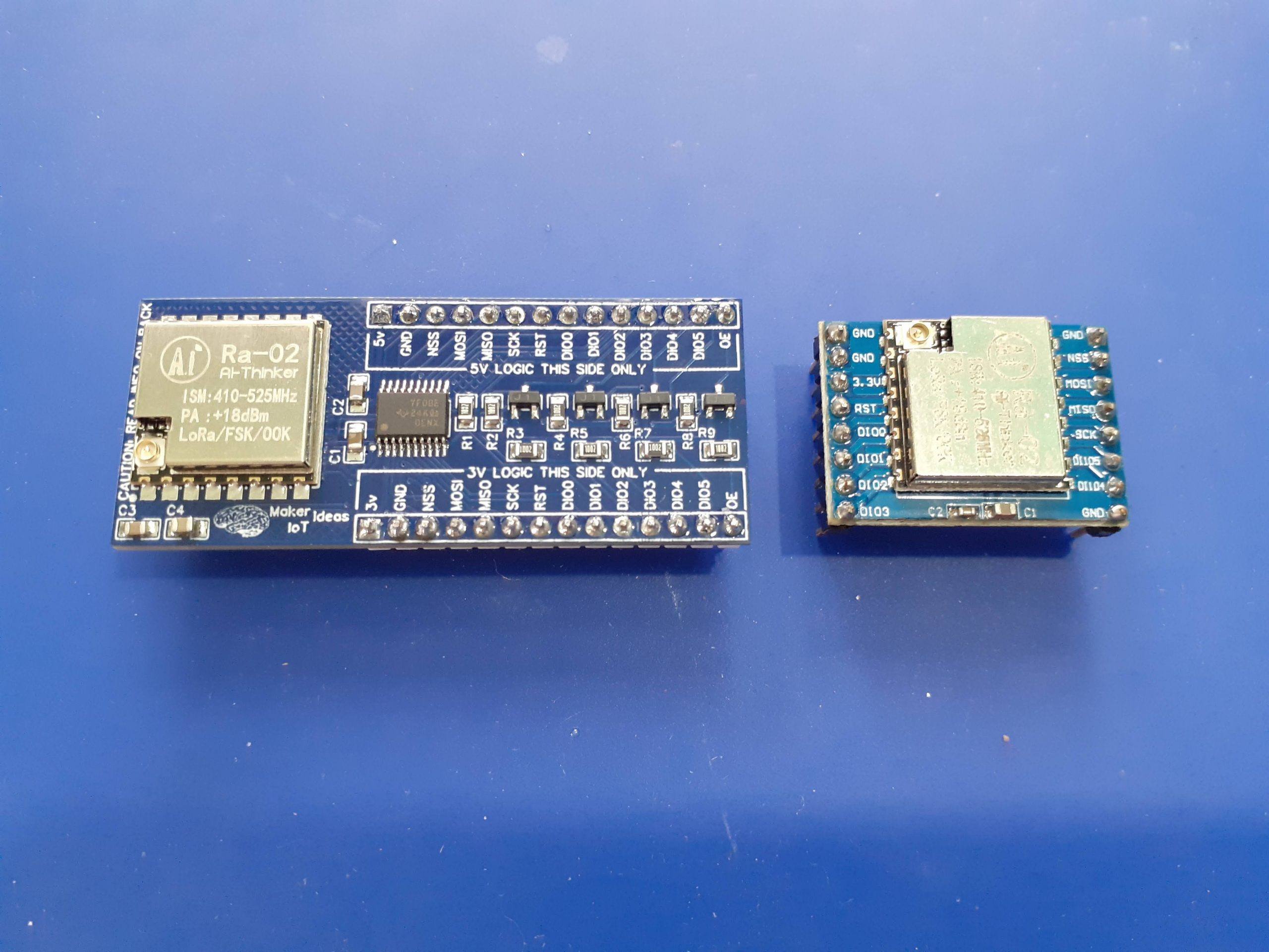
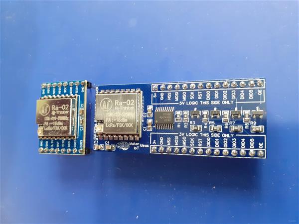
Most Makers and electronics enthusiasts may already know of the RA-02 LoRa Module. Many of them might own an RA-02 Breakout module or two… For those who do, they will surely know about the problems encountered with using this particular breakout module…
The RA-02 module, in itself, is a great piece of kit, and when used on a custom PCB, which was designed with all the little secrets of this module taken into consideration, is a pleasure. Using the RA-02 breakout module, in its existing form factor, does however present quite a few unique challenges, which, if you are unaware of them, can cause quite a few frustrating moments, or even result in permanent damage to the module…
1) The module is based on the SX1278 chip from Semtech and is a 3v device. The IO pins are NOT 5v compatible but seem to work for a few hours or so when used with 5v… This causes many people, especially on Youtube, to assume that it is ok to send 5v logic signals to this module…
I have still not seen any Youtube video telling viewers to at least use a resister divider or logic converter… People just don’t know, and those that know seem to be keeping quiet!
Adding logic converters is in fact specified by the datasheet.
2) Adding logic converters means adding additional wiring, and for a breadboard based project, that adds to the complexity.
3) You have a total of 4 ground pins that need to be connected. not connecting all of them, causes funny things to happen, from overheating down to failure… ( My personal experience while researching this project)
4) The existing breakout module is not breadboarding compatible, resulting in a floating assembly with wires going everywhere, which results in unstable connections etc…
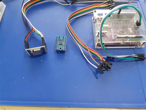
Basically something similar to the picture below:
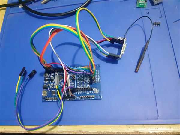
In this picture, I have an existing RA-02 Breakout Module, with an 8 channel Logic converter and an Arduino Uno clone, along with all the needed wiring to make this setup possible… Quite a lot of wires indeed…
My solution:
I design and use quite a few LoRa PCBs and on all of them, I implement logic conversion using the BSS138 N-MOS Mosfet and 10k resistors. It is a cheap and reliable solution, but it can take up quite a lot of space on a PCB, as this means 11 Mosfets and 22 10k resistors if I were to provide level conversion to all of the RA-02’s GPIO and IO pins…
I also have the constant problem of many unnecessary wires, many of which sometimes fail straight out of the box, when prototyping something. I partly solved that by designing a few dedicated PCB solutions, but that is not always ideal,
Using a dedicated Logic Converter IC, and Mosfet based converters to make up the difference, on a breadboard compatible module, seemed like a good idea, so I went ahead and designed the following solution:
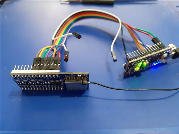
The breakout board module is breadboard compatible, and also has clearly marked pins to indicate the 3v and 5v sides of the module.
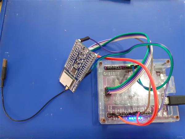
For my first test, I decided to test with an Arduino Uno Clone, since that is what most Makers and students will have access to. I used Cytron’s Maker Uno platform, which is equipped with some added goodies, in the form of diagnostic LED etc to make prototyping a lot easier.
As we can clearly see, It is only necessary to connect to the 5v logic side of the module, as well as provide 3v and 5v + GND to the module
In this test, I used Sandeep Mistry’s LoRa Library, with the Arduino IDE to do a quick test sketch.
As we can see, you need quite a lot more wires to make this work. It is also worth noting that we have only 8 level converters on this ATMEGA328P PCB, in order to use all of the RA-02’s GPIO, we will need to add an additional external logic converter as well.
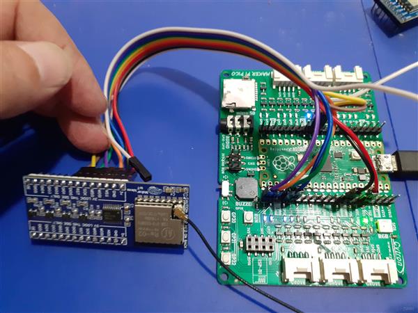
For my second test, I decided to be a bit brave, and try to use the new Raspberry Pi Pico ( RP2040 Microprocessor ). I have quite a few of them lying around and have never really done a lot with them, due to the fact that I do not really like using MicroPython or CircuitPython, and also because the recently released Arduino Core for the RP2040 still being quite new… I decided to use a development board that I recently bought from Cytron, the Maker Nano RP2040, as it has all the added diagnostic features to make my life a bit easier, I will also include a test with an original Pi Pico board, to make it more accessible to everyone out there.
Once again, I used Sandeep Mistry’s LoRa Library, with the exact same Arduino sketch, used for the Maker Uno test. (I obviously needed to change the pin numbers though, as the RP2040 uses different pins for its SPI interface).
Maker Nano RP2040 RA-02 Breakout Module
NSS 17
MOSI 19
MISO 16
SCK 18
RST 9
DIO0 8
In this case, we DO NOT need the OE pin, as the RP2040 is a native 3v device. The level converter can thus stay disabled, with its pins in tri-state ( high impedance ) mode.
If we look at the code, it is similar to the Maker Uno’s code, with only the Pin declarations needing a change
#include <SPI.h> // include libraries
#include <LoRa.h>
const int csPin = 17; // LoRa radio chip select
const int resetPin = 9; // LoRa radio reset
const int irqPin = 8; // change for your board; must be a hardware interrupt pin
byte msgCount = 0; // count of outgoing messages
int interval = 2000; // interval between sends
long lastSendTime = 0; // time of last packet send
// Note that SPI has different names on the RP2040, and it has 2 SPI ports. We used port 0
// CIPO (Miso) is on pin 16
// COPI (Mosi) is on pin 19
// SCK is on pin 18
// CE/SS is on pin 17, as already declared above
I did not use a breadboard, in order to make things as easy as possible.
To make things a bit easier, without having to resort to using a breadboard, I decided to do the Original Pi Pico test using the Maker Pi Pico PCB. This PCB is basically a big breakout module, with detailed pin numbers and some diagnostic LEDs, but it also uses a native Pi Pico, soldered directly to the PCB, by means of the castellated holes… So, While technically not being a true standalone Pico, It makes my life easier and was thus used for the test, as I can be sure that the pins are labelled exactly the same as on the original Pico.
The code used for the Maker Nano RP2040 works perfectly, with no changes required.
This post is getting quite long by now, so I have decided not to include my tests of the ESP-12E ( NodeMCU ) or ESP32 development boards here as well… They also function as expected.
In Summary
When I started this project, I set out to solve a problem ( personal to me ), that could potentially help a lot of other people use the RA-02 Module for more projects and tasks. The Breakout module in its current form can also be used with the RA-01h module (915Mhz Module) without any changes. All GPIO pins are broken out, and accessible through full logic converted pins on both sides of the breakout module.
I hope that this will be useful to someone. I am also not releasing the full schematics at this stage, as I may decide to make some minor cosmetic changes in the near future.
The PCB can however be ordered from PCBWay in its current form and works 100% as expected. The BOM file is available with the ordered PCB as usual.
This PCB was manufactured at PCBWAY. The Gerber files and BOM, as well as all the schematics, will soon be available as a shared project on their website. If you would like to have PCBWAY manufacture one of your own, designs, or even this particular PCB, you need to do the following… 1) Click on this link 2) Create an account if you have not already got one of your own. If you use the link above, you will also instantly receive a $5USD coupon, which you can use on your first or any other order later. (Disclaimer: I will earn a small referral fee from PCBWay. This referral fee will not affect the cost of your order, nor will you pay any part thereof.) 3) Once you have gone to their website, and created an account, or login with your existing account,
4) Click on PCB Instant Quote
5) If you do not have any very special requirements for your PCB, click on Quick-order PCB
6) Click on Add Gerber File, and select your Gerber file(s) from your computer. Most of your PCB details will now be automatically selected, leaving you to only select the solder mask and silk-screen colour, as well as to remove the order number or not. You can of course fine-tune everything exactly as you want as well.
7) You can also select whether you want an SMD stencil, or have the board assembled after manufacturing. Please note that the assembly service, as well as the cost of your components, ARE NOT included in the initial quoted price. ( The quote will update depending on what options you select ).
8) When you are happy with the options that you have selected, you can click on the Save to Cart Button. From here on, you can go to the top of the screen, click on Cart, make any payment(s) or use any coupons that you have in your account.
Then just sit back and wait for your new PCB to be delivered to your door via the shipping company that you have selected during checkout.
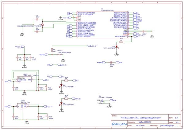
ATMEGA328P Module with integrated LoRa and CAN-BUS
INTRODUCTION
In my quest to perfect my LoRa telemetry system, I have gone through quite a few prototypes by this time. This post will focus on the next node design. Due to the fact that the area where I will deploy the system is quite large, but with roughly square boundary fence-lines, I decided to try and reduce the number of LoRa Radio nodes needed to cover the entire area. This opened up the opportunity to utilise CAN-BUS to attach sensor-only nodes to a Radio node and have them report status on exception as well as on requests from the radio node.
The device will thus function as a LoRa-to-CAN-BUS Gateway, with some local automation to control the transmission of data to the master station. This concept can also be adapted for use in other areas, such as home -automation, or an industrial setting.
At the heart of the device, I have stuck with the versatile ATMEGA328P, which, current chip shortages excluded, and current high prices excluded, are a very inexpensive chip, with lots of well-tested libraries, and a relatively low learning curve, largely due to its very wide use in the Arduino ecosystem.
The LoRa component is handled by the RA-02 or even RA-01H module, from AI-Tinker (not sponsored). This device, as we have seen in the previous prototypes, requires the use of logic level converters, due to the fact that it only accepts 3.3v logic levels. While I could get rid of those if I powered the ATMEGA328P from 3.3v, it would give rise to two problems, of which one will still force the use of level converters…
I chose to run the ATMEGA328P at 16Mhz, which basically forces me to use 5v to power the chip. The second reason is not so obvious unless you read a few datasheets very thoroughly…
The CAN-Bus component is handled by the MCP2515 Standalone SPI-to-CAN Controller, as well as the TJA1050 CAN Bus transceiver.
This is where things get interesting… The MCP2515 can operate on 3.3v, but the TJA1050 is a 5v only device. I could thus in theory use logic level converters only between the MCP2515 and the TJA1050, while running the rest of the circuit on 3.3v…
Given that I would rather run the ATMEGA328P on 16Mhz, as well as the fact that my LoRa Radio Module circuit, with its logic level converter circuitry, works extremely well, I decided not to change that, and keep the CAN Bus running at 5v all the way through, as I would still have to use a 5v regulator on the PCB anyway just for that purpose.
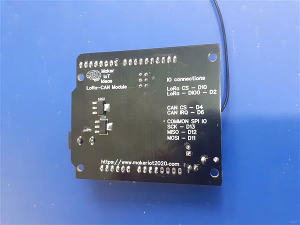
IO connections for LoRa and CAN BUS modules
You can order this PCB directly from PCBWay, by clicking here
Both of the two integrated components ( Lora and CAN ) are SPI devices. This means that they share common SCK, MISO and MOSI lines ( provided on the ATMEGA328P by pins D13, D12 and D11 respectively. The individual SPI device is then further selected for operation by the use of a CE pin, one unique pin per device, which is pulled low by the MCU to indicate to the device that it should pay attention to the data being transmitted on the SPI bus…
Both LoRa and CAN makes use of other pins as well, LoRa needs a Reset pin, connected to D9, a CS/CE Pin on D10 as well as a hardware interrupt pin, connected to D2. ( Note that this is for use with Sandeep Mistry’s LoRa Library. The Radiolib library would require an additional pin, usually connected to DIO1 on the LoRa module. The device does not provide access to those pins in its current layout, so you can only use it with the Sandeep Mistry library, for now at least… )
The CAN module uses a CE/CS pin at D4, with an IRQ pin on D6, which, although not a hardware interrupt pin, does have PCINT functionality.
Pins D10, D9 and D2 are not broken out for user access. although I decided to give access to D4 and D6, as well as the SPI bus, D11, D12, D13, to allow interfacing with logic analysers, or adding other SPI devices to the bus…
This brings us to a very interesting point… Does the two SPI devices actually play nice together? and what do I mean by “playing nice together”?
To answer that question, we are forced to first look at a bit of theory, as well as understand the fundamental differences between SPI and I2C…
The Difference between SPI and I2C
Most of us will be quite familiar with I2C, as it is a very common protocol used to connect sensors to a microcontroller. It consists of only two IO lines, SDA for data, and SCL for the clock. Each device on the bus has its own built-in address, like in the case of a PCF8574 IO expander, this address can be selectable between 0x20h and 0x27h. All of the devices share these common data lines, and will only respond when specifically addressed by the master controller… Unless you accidentally put two devices with the same address on the same bus, (if that would even work), there is no way that the wrong device would respond to any request for data…
SPI on the other hand, operates on a completely different principle, making it quite a few times faster than I2c, with data being simultaneously sent and received by the active device… SPI is also known as a four-wire protocol. Each device has a minimum of 4 data lines, namely SCK ( clock), MOSI ( for data transmitted FROM the Master TO the slave device ), MISO ( for data transmitted TO the master FROM the slave device) and a CE or CS ( Chip select ) pin.
SCK, MISO and MOSI are COMMON to all devices, meaning it is shared between all of them. CE/CS is a unique pin for EACH device, meaning that if you had four SPI devices on a bus, you would have to have four individual CE/CS pins!
A device will, or rather should only respond to data on the SPI-BUS IF the master pulls its respective CE/CS pin LOW. It should now very quickly become clear to you that this can become a very very complex mess, very quickly.
Let us take a very good example. the ST7789 SPI display module, has a cheap version, commonly sold on Ali-express, as we ll as other online stores. This particular module, I assume in a bid to make it easier to use, has the CE/CS pin internally pulled down to ground by default… So what about that, you may ask? What is wrong with that, as it saves you an IO pin?
It is in fact very wrong, a fact that you will very quickly discover if you ever tried using one of those displays on an SPI bus together with other SPI devices… Nothing will work, or only the display will work ( if you are lucky)
But why?
Pulling CE/CS LOW, signals to the chip that it should respond to instructions on the common SCK, MISO and MOSI lines. having the pin internally pulled LOW, thus forces that chip to always respond, even when it should not. Thus contaminating the entire SPI-BUS with garbage…
The answer to the question
After that very long-winded explanation, which is still extremely basic, it is time that we get back to our original question:
Does the Sx127x ( RA-02 ) Module and the MCP2515 Can Controller play nice on the same bus? The answer is not straightforward, as it comes down to which libraries you use…
Remember that the library must pull down the CE/CS pin of the device that it wants to communicate with. Some libraries wrongly assume that they are the only ones in use, and ignores the simple fact, that they should release the CE/CS pin AFTER EVERY transaction, to free up the bus for other devices to use it as well…
After extensive testing, I can however say that Sandeep Mistry’s LoRa Library, as well as the mcp_can library, does indeed play nice together. These two libraries do not keep the individual CE/CS pins pulled LOW, and allows the spi bus to be shared.
This is not the case with the ST7789 Module discussed above, where the hardware actually pulls the pin ow the entire time…
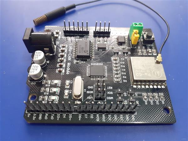
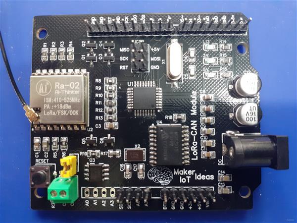
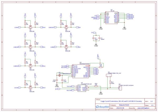
Taking a closer look at the PCB
Let us take a closer look at the PCB. The Ra-02 Module ( LoRa ) dominates most of the left-hand side of the PCB, with the ATMEGA328P on its right. The RA-02 is surrounded by the level converters, using the BSS138 N-Channel Mosfet, and 10k resistors (Q1 to Q6, R1, R2, R3, R4, R5, R6, R8, R9, R10, R11, R12, R13)
C1 and C2 are bypass capacitors for the Ra-02 module
In the bottom left corner, we have a hardware reset button, to reset the ATMEGA328P, with a yellow jumper (H1) next to it. This jumper controls the 120ohm ballast resistor (R17) for the CAN bus. Removing the jumper will remove the ballast. Directly below that is the CAN connecter, marked as U5, with CH as CAN-H, and CL as CAN-L ports.
U3 and U4, together with R18, R19, X2, C16, C17 make up the CAN components on the PCB. Decoupling is provided by C6, C7, C8 as well as C9 and C12 ( Includes the ATMEGA328P’s decoupling as well )
An ICSP programming header is provided above U1 ( ATMEGA328P) for use with USPASP, AVRASP or Arduino as ISP and similar.
No USB to serial converter is provided on the board, Serial upload is possible is loaded with an Arduino bootloader for the Arduino NANO ( to make use of all the analog inputs). RxD, TxD and DTR pins are broken out on opposite sides of the PCB, as well as access to 3.3v, 5v and GND pins.
A DC power socket is provided. it can accept up to 12v DC, although I would recommend not to go over 7.2 volts, to not stress the LDO regulators, at the back of the PCB ( LDO1, and LDO2) too much.
You can order this PCB directly from PCBWay, by Clicking here
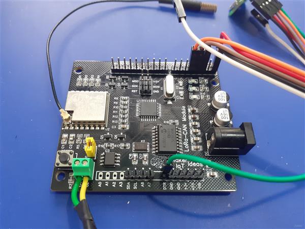
in the picture above, I have connected a USB-to Serial converter, as well as CAN-BUS to the device.
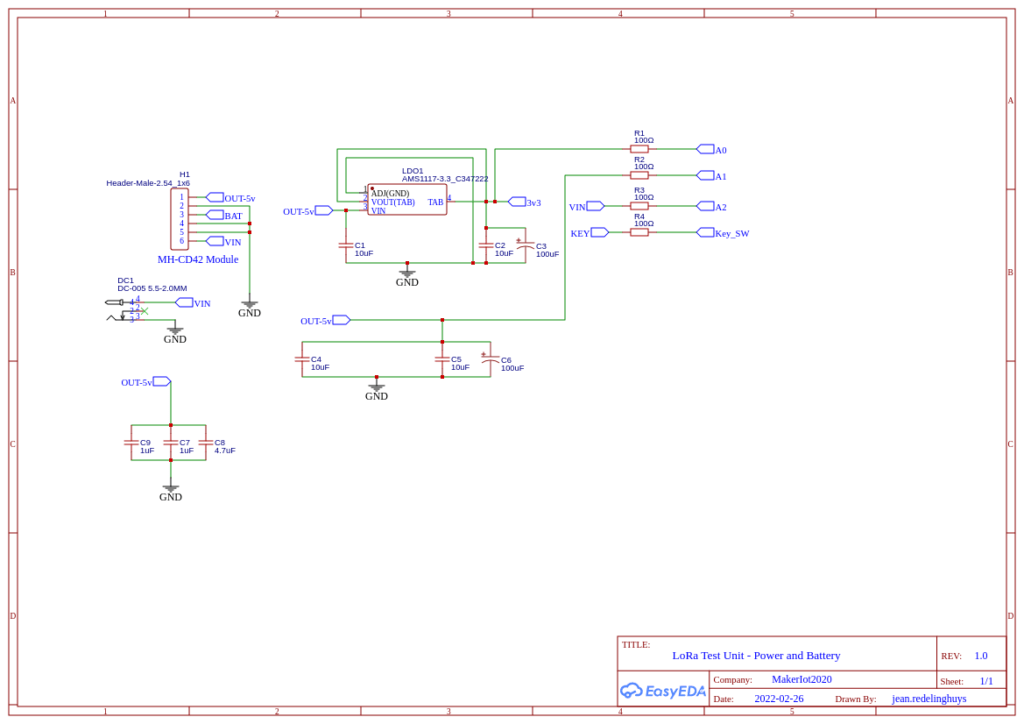
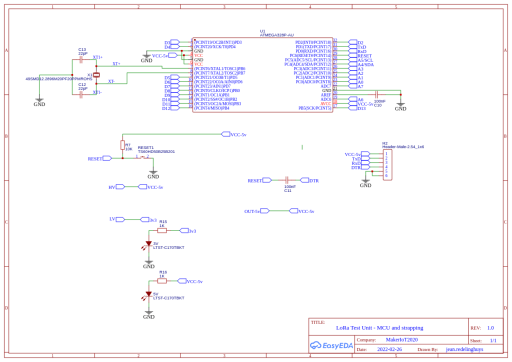
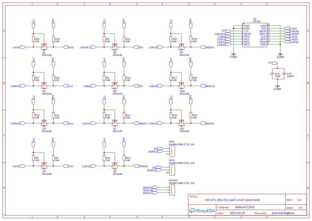
Schematic Diagram
The detailed schematic diagrams are provided below:
Sheet 1 (above) takes care of the ATMEGA328p and it supporting circuitry, as well as the power supply via LDO regulators.
Sheet 2 (below) takes care of the Logic Level converters, RA-02 (Sx1278) LoRa Module, and CAN-BUS controller and transceiver circuitry.
A combined example utilising both LoRa and CAN at the same time, will be released with the next part of the project, namely the CAN-Relay Module
This PCB was manufactured at PCBWAY. The Gerber files and BOM, as well as all the schematics, will soon be available as a shared project on their website. If you would like to have PCBWAY manufacture one of your own, designs, or even this particular PCB, you need to do the following… 1) Click on this link 2) Create an account if you have not already got one of your own. If you use the link above, you will also instantly receive a $5USD coupon, which you can use on your first or any other order later. (Disclaimer: I will earn a small referral fee from PCBWay. This referral fee will not affect the cost of your order, nor will you pay any part thereof.) 3) Once you have gone to their website, and created an account, or login with your existing account,
4) Click on PCB Instant Quote
5) If you do not have any very special requirements for your PCB, click on Quick-order PCB
6) Click on Add Gerber File, and select your Gerber file(s) from your computer. Most of your PCB details will now be automatically selected, leaving you to only select the solder mask and silk-screen colour, as well as to remove the order number or not. You can of course fine-tune everything exactly as you want as well.
7) You can also select whether you want an SMD stencil, or have the board assembled after manufacturing. Please note that the assembly service, as well as the cost of your components, ARE NOT included in the initial quoted price. ( The quote will update depending on what options you select ).
8) When you are happy with the options that you have selected, you can click on the Save to Cart Button. From here on, you can go to the top of the screen, click on Cart, make any payment(s) or use any coupons that you have in your account.
Then just sit back and wait for your new PCB to be delivered to your door via the shipping company that you have selected during checkout.
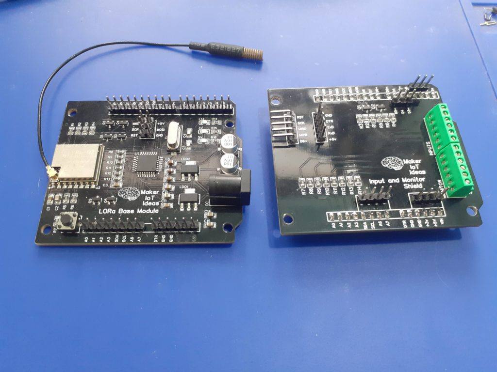
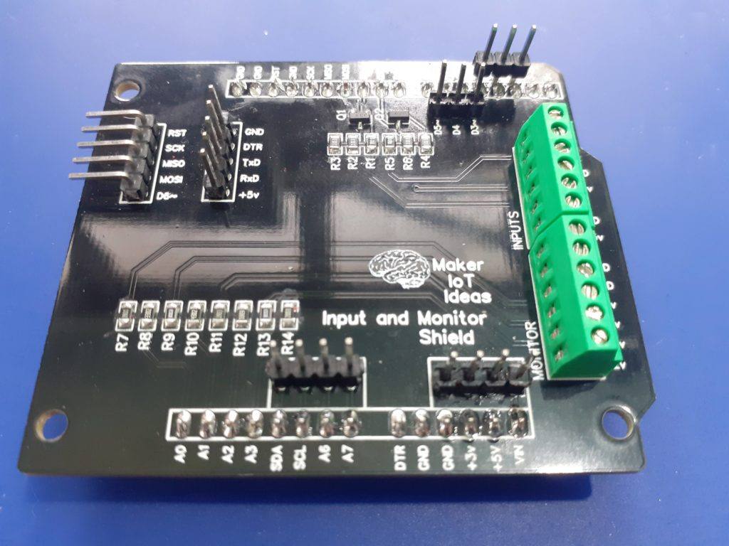
This is a straightforward project compared to my usual PCB projects. It is one of a series of designs towards completing my LoRa monitoring system, that I plan to use on the farm to monitor various areas, such as intrusion detection, battery levels etc.
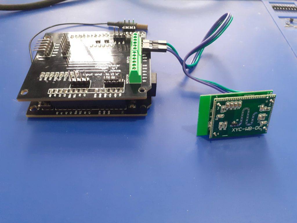
The shield was designed to fit on top of the first LoRa Base Module. It was designed to allow easy, neat connections to Infrared Beam sensors, XYC-WB-DC Motion Detector, as well as to monitor the battery levels at the Solar power inverter (the farm is completely off-grid).
The Motion Sensor provides a +3v signal that goes high on motion detection, while the Infrared Beam Sensor provides a relay contact that can be used to provide a similar voltage signal. As I prefer to use pull-up logic on my inputs, I decided to implement a simple transistor circuit where the input will switch the base of the transistor, which in turn will pull the input to signal ground when switched on. This circuit uses the S8050 transistor, with the base pulled down to signal ground via a 10k resistor to prevent floating, and a current limiting resistor of 1k to 1k8 on the base. The collector, as well as the D7 and D8 GPIO pins on the LoRa Base Module, is pulled High to Vcc5v via a 10k resistor.
Voltage monitoring is done with the ADC on the LoRa Base Module, with each of the 4 battery levels ( 12v, 24v,36v, and 56v) being connected to the relevant ADC channel via a resister-divider network to lower the respective voltage to a level between 0 and 5v. ( This was done as the ADC on the ATMEGA328p can only handle a maximum voltage of 5.0v )
The resistors were chosen to give a slightly bigger input voltage range, to accommodate for fluctuations from the solar charger ( It can sometimes go up to 65v on a very bright sunny day ). I decided to not add any current limiting resistors directly onto the PCB, as they are definitely going to be bulky. They will instead be attached externally, to suitable heatsinks, etc…
As this PBC is still in the prototype stage, and my LoRa Monitoring device will definitely go through quite a few modifications in future, I provided access to all unused GPIO pins via separate headers on the shield. Most notably the SPI Header, used for programming the ATMEGA328P MCU, or connecting other SPI devices ( I am working on a CAN bus addon for the device, to save on the number of physical radio nodes that needs to be installed), The UART Header, as well as I2C, A6, A7 and additional Digital IO Pins (D3~, D4, D5~).
In the photo above you will notice an additional header on the UART pins, This was added to assist me with debugging on the logic analyser, as I had a slight issue with waking up the ATMEGA328P, and getting it to send events via LoRa. It would wake up, print status messages through the UART, but never do the actual LoRa part! That has now been fixed, and the header removed…
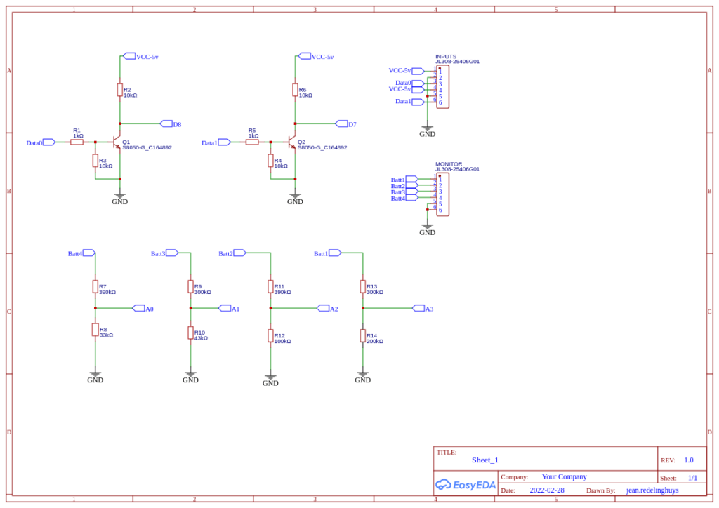
The schematic diagram for the shield is below. As you will see, it is very uncomplicated indeed.
The RA-02 Module (SX1278) connections to the ATMEGA328p is as follows:
NSS to D10 (CE)
MOSI to D11 (MOSI)
MISO to D12 (MISO)
SCK to D13 (SCK)
RESET to D9
DIO0 to D2 ( We need a hardware Interrupt pin ).
DIO1 to DIO5 was not broken out on the current version of the LoRa Base Module
There is also no direct access to pins D10, D9 and D2 either on the LoRa Base Module or on the Input and Monitor Shield.
If you do decide to hack the device and add access to any of the non broken out pins, please remember to use a logic level converter between the ATMEGA328 and the SX1278, as they operate at different voltages, and the SX1278 is not 5v tolerant on any of the IO Pins!
You can order this shield from PCBWay by clicking here
This PCB was manufactured at PCBWAY. The Gerber files and BOM, as well as all the schematics, will soon be available as a shared project on their website. If you would like to have PCBWAY manufacture one of your own, designs, or even this particular PCB, you need to do the following… 1) Click on this link 2) Create an account if you have not already got one of your own. If you use the link above, you will also instantly receive a $5USD coupon, which you can use on your first or any other order later. (Disclaimer: I will earn a small referral fee from PCBWay. This referral fee will not affect the cost of your order, nor will you pay any part thereof.) 3) Once you have gone to their website, and created an account, or login with your existing account,
4) Click on PCB Instant Quote
5) If you do not have any very special requirements for your PCB, click on Quick-order PCB
6) Click on Add Gerber File, and select your Gerber file(s) from your computer. Most of your PCB details will now be automatically selected, leaving you to only select the solder mask and silk-screen colour, as well as to remove the order number or not. You can of course fine-tune everything exactly as you want as well.
7) You can also select whether you want an SMD stencil, or have the board assembled after manufacturing. Please note that the assembly service, as well as the cost of your components, ARE NOT included in the initial quoted price. ( The quote will update depending on what options you select ).
8) When you are happy with the options that you have selected, you can click on the Save to Cart Button. From here on, you can go to the top of the screen, click on Cart, make any payment(s) or use any coupons that you have in your account.
Then just sit back and wait for your new PCB to be delivered to your door via the shipping company that you have selected during checkout.
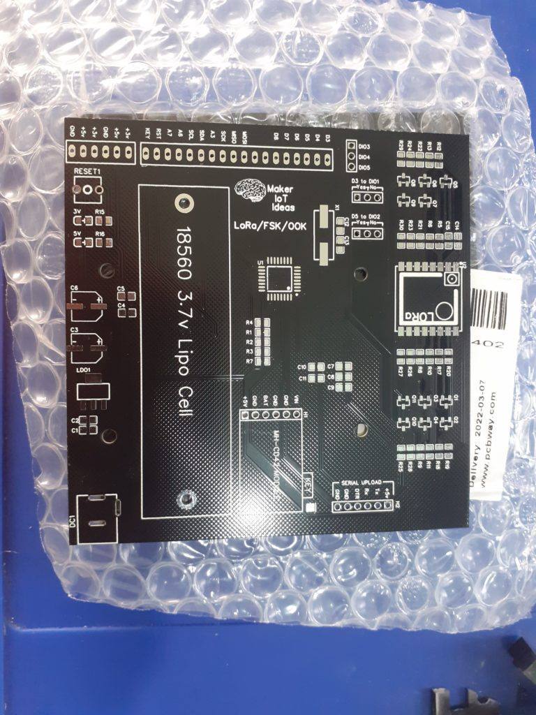
SX127x LoRa/FSK/OOK Module with LiPo battery-backup
SX127x LoRa/FSK/OOK Prototype Radio Board
I recently had a requirement to do some automation/telemetry on the farm. Things went missing, unauthorised persons were trespassing on the property, helping themselves to eggs, chickens, ducks and produce. Something had to be done, and as there is nobody sleeping there at night, it had to be possible to get remote status updates in real-time.
The farm is also completely off-grid, with solar-powered inverters taking care of all the water and electricity needs. Power usage monitoring could thus be a great help as well…
The idea is as follows:
Have a central control station, with various remote devices to do intrusion detection, control lights and water pumps, as well as monitor the battery levels of the inverter and solar-panel system. As the area is quite large, having to pull in electrical cabling will not be feasible, nor could the inverter handle all of that.
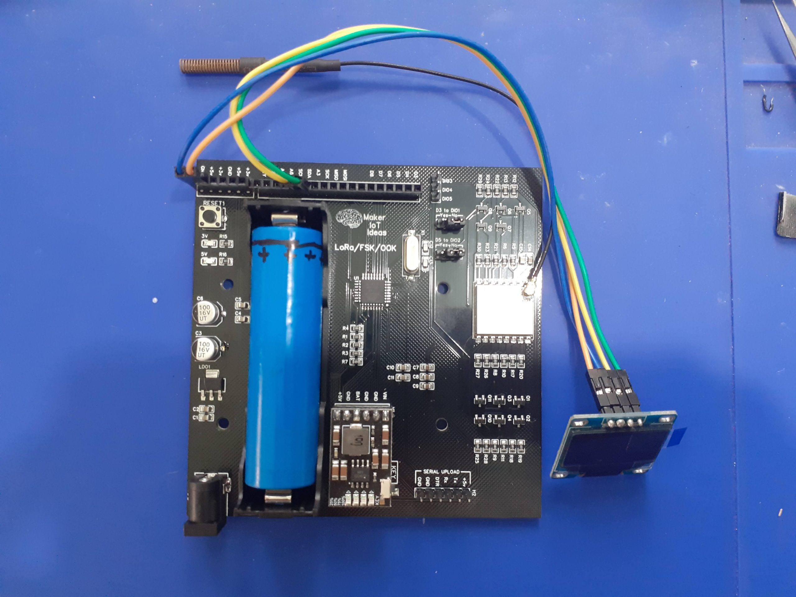
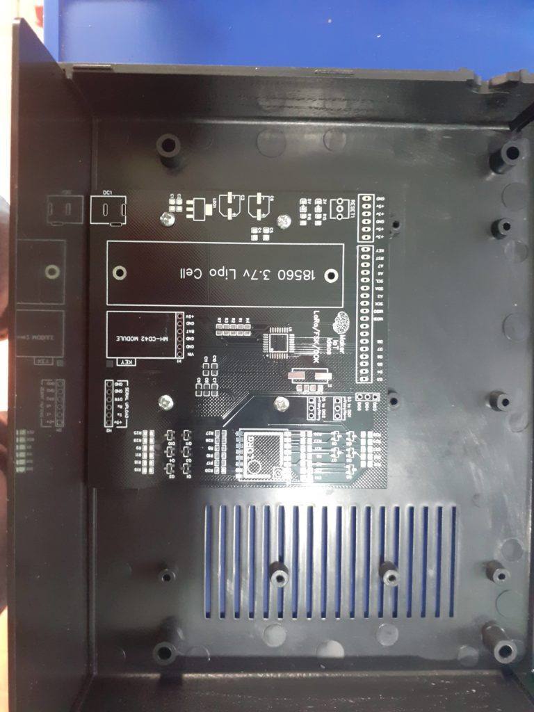
I decided to use the RA-02 LoRa/FSK/OOK module, on a custom PCB, but with various different PCB modifications, to take care of each stage of the project. The PCB that I will present today will be mainly used as the control unit, but it could also be a remote station, depending on what options are needed.
The ATMEGA328P-AU MCU is used as the main processor on each board, with the MH-CD42 Boost Converter/LiPo battery charger module taking care of power supply requirements. This module can source up to 2A at 5.0v, More than adequate for my needs. The ATMEGA328P will be put into sleep mode, to wake on interrupt to respond to events as needed ( To help save power ). Power usage of the circuit is around 50mA in standby ( NOT SLEEP MODE ), and with a peak of 100mA on a LoRa Transmit or Receive event.
The RA-02 Module did however present some challenges, as it is a 3.3v device, with non-5v capable IO lines. This made it necessary to include a 3.3v LDO regulator, as well as logic level converting circuitry onto the PCB. To allow for the most flexibility, all DIOs on the RA-02 was also broken out via level converters, in addition to the required SPI pins ( MOSI, MISO, CE and SCK ). This amount to a total of 11 level converters onboard.
I chose the MH-CD42 Power module for the reason that it can supply current at the same time as charging the LiPo battery (in my case, I used a 18650 cell). This will help greatly, as 220v inverter power is available during the day to charge the batteries.
Another challenge was definitely the enclosure. I found some really nice enclosures online, but the mounting holes were located in a very particular pattern, making it necessary to do some very careful measuring to get the PCB to fit exactly. The enclosure also has space to accept the other PCB modules, like the USER Control panel, and other sensor devices as needed. PCBWay did a great job at manufacturing the PCB so as to fit exactly. I must admit that I had quite a few tense moments between sending the PCB off to manufacturing and receiving it, as to whether my measurements were actually accurate, and if the PCB would fit as I imagined…
As you can see in the picture above, it turned out perfectly.
The Circuit diagram is basically a standard Arduino Nano ( I needed access to all of the ADC pins ),
Connections to the RA-02 module is as follows:
RA-02
ATMEGA328P
MOSI
D11
MISO
D12
SCK
D13
CE
D10
RESET
D9
DIO0
D2 ( We need a hardware interrupt pin here )
DIO1
D3 ( Hardware Interrupt, enabled through jumper)
DIO2
D5 ( Enabled through a jumper)
DIO3 to DIO 5
Not connected, available on a breakout header
Connections between Ra-02 (SX127x) and ATMEGA328P – Note that all IO Lines are connected through level converters 5v <-> 3.3v
On the ATMEGA328, the following pins are broken out into headers:
D3
can be connected to RA-02 with a jumper
D4
D5
can be connected to RA-02 with a jumper
D6
D7
D8
D13 ( SCK )
Broken out as a 5v logic pin
D12 ( MISO )
5v logic pin
D11 ( MOSI )
5v logic pin
A3,A6,A7
ADC Pins ( A0, A1, A2 is used internally to monitor VIN, VCC5v and VCC3v ) A0 = Vcc3v A1 = Vcc5v A2 = VIN
SCL
I2C SCL pin OR A5 (I2C pins are at 5v logic levels )
SDA
I2C SDA pin OR A4 (I2C pins are at 5v logic levels )
RESET
DTR
( connected through a 100nf Cap to Reset, used for serial uploading firmware )
D0 ( RxD )
UART Rx Pin ( 5v logic )
D1 ( TxD )
UART Tx Pin ( 5v logic )
ATMEGA328P breakout pins. All pins are at 5v logic level
The ATMEGA328P is clocked at 16Mhz through an external crystal.
3v, 5v and GND pins were broken out at two opposite corners of the PCB to allow easy connection of additional devices/ sensors as needed.
The MH-CD42 module has the capability to power a load while charging the LiPo battery. This makes it possible to do a few interesting things while supplying power to this particular PCB.
The board can be powered directly from a 5v header pin ( NOT from the DC1 input ). In this mode, a LiPo battery is not required.
5v will be directly supplied to the processor, as well as the 3.3v LDO regulator, allowing the RA-02 module to function as well.
PLEASE NOTE: THERE ARE NO 5v REGULATION – MAKE SURE YOU SUPPLY REGULATED 5v
Installing the MH-CD42 module will add the option of charging a 3.3v 18650 Lipo battery, as well as powering the board at the same time. You need to supply power through the DC plug to make use of this function. This mode is also a miniature uninterruptible power supply, with the 3.3v LiPo battery immediately taking over should the main DC input fail.
NOTE: The MH-CD42 can only accept up to 5.5v MAXIMUM as input!
Software:
The PCB can be used with LoRa libraries from Sandeep Mistry OR JGromes/RadioLib ( If you want to do FSK/OOK or other advanced stuff like LoRa of FHSS)
Both libraries have extensive examples showing how to use them. As our use case will definitely differ, I will not have any example here at this stage. I will add one later after the entire project is completed, with all the relevant modules.
This PCB was manufactured at PCBWAY. The Gerber files and BOM, as well as all the schematics, will soon be available as a shared project on their website. If you would like to have PCBWAY manufacture one of your own, designs, or even this particular PCB, you need to do the following… 1) Click on this link 2) Create an account if you have not already got one of your own. If you use the link above, you will also instantly receive a $5USD coupon, which you can use on your first or any other order later. (Disclaimer: I will earn a small referral fee from PCBWay. This referral fee will not affect the cost of your order, nor will you pay any part thereof.) 3) Once you have gone to their website, and created an account, or login with your existing account,
4) Click on PCB Instant Quote
5) If you do not have any very special requirements for your PCB, click on Quick-order PCB
6) Click on Add Gerber File, and select your Gerber file(s) from your computer. Most of your PCB details will now be automatically selected, leaving you to only select the solder mask and silk-screen colour, as well as to remove the order number or not. You can of course fine-tune everything exactly as you want as well.
7) You can also select whether you want an SMD stencil, or have the board assembled after manufacturing. Please note that the assembly service, as well as the cost of your components, ARE NOT included in the initial quoted price. ( The quote will update depending on what options you select ).
8) When you are happy with the options that you have selected, you can click on the Save to Cart Button. From here on, you can go to the top of the screen, click on Cart, make any payment(s) or use any coupons that you have in your account.
Then just sit back and wait for your new PCB to be delivered to your door via the shipping company that you have selected during checkout.
In this part of my LoRa Series ( Part 3 ) I will look at some basic code for the Heltec LoRa 32 V2 Module. This code will in particular be focused on Multiple device communication. It can easily adapted from the stock example (as provided below) to implement a custom addressing scheme.
LoRa Multiple Communications No Interrupt
#include "heltec.h"

#define BAND    433E6  //you can set band here directly,e.g. //868E6,915E6


String outgoing;              // outgoing message

byte localAddress = 0xBB;     // address of this device
byte destination = 0xFD;      // destination to send to

byte msgCount = 0;            // count of outgoing messages
long lastSendTime = 0;        // last send time
int interval = 2000;          // interval between sends

void setup()
{
   //WIFI Kit series V1 not support Vext control
  Heltec.begin(true /*DisplayEnable Enable*/, true /*Heltec.LoRa Enable*/, true /*Serial Enable*/, true /*PABOOST Enable*/, BAND /*long BAND*/);

  Serial.println("Heltec.LoRa Duplex");


}

void loop()
{
  if (millis() - lastSendTime > interval)
  {
    String message = "Hello there!";   // send a message
    sendMessage(message);
    Serial.println("Sending " + message);
    lastSendTime = millis();            // timestamp the message
    interval = random(2000) + 1000;    // 2-3 seconds
  }

  // parse for a packet, and call onReceive with the result:
  onReceive(LoRa.parsePacket());
}

void sendMessage(String outgoing)
{
  LoRa.beginPacket();                   // start packet
  LoRa.write(destination);              // add destination address
  LoRa.write(localAddress);             // add sender address
  LoRa.write(msgCount);                 // add message ID
  LoRa.write(outgoing.length());        // add payload length
  LoRa.print(outgoing);                 // add payload
  LoRa.endPacket();                     // finish packet and send it
  msgCount++;                           // increment message ID
}

void onReceive(int packetSize)
{
  if (packetSize == 0) return;          // if there's no packet, return

  // read packet header bytes:
  int recipient = LoRa.read();          // recipient address
  byte sender = LoRa.read();            // sender address
  byte incomingMsgId = LoRa.read();     // incoming msg ID
  byte incomingLength = LoRa.read();    // incoming msg length

  String incoming = "";

  while (LoRa.available())
  {
    incoming += (char)LoRa.read();
  }

  if (incomingLength != incoming.length())
  {   // check length for error
    Serial.println("error: message length does not match length");
    return;                             // skip rest of function
  }

  // if the recipient isn't this device or broadcast,
  if (recipient != localAddress && recipient != 0xFF) {
    Serial.println("This message is not for me.");
    return;                             // skip rest of function
  }

  // if message is for this device, or broadcast, print details:
  Serial.println("Received from: 0x" + String(sender, HEX));
  Serial.println("Sent to: 0x" + String(recipient, HEX));
  Serial.println("Message ID: " + String(incomingMsgId));
  Serial.println("Message length: " + String(incomingLength));
  Serial.println("Message: " + incoming);
  Serial.println("RSSI: " + String(LoRa.packetRssi()));
  Serial.println();
}
LoRa Multiple communication, Interrupt
#include "heltec.h"

#define BAND    433E6  //you can set band here directly,e.g. 868E6,915E6


byte localAddress = 0xBB;     // address of this device
byte destination = 0xFF;      // destination to send to

String outgoing;              // outgoing message
byte msgCount = 0;            // count of outgoing messages
long lastSendTime = 0;        // last send time
int interval = 2000;          // interval between sends

void setup()
{
   //WIFI Kit series V1 not support Vext control
  Heltec.begin(true /*DisplayEnable Enable*/, true /*Heltec.LoRa Disable*/, true /*Serial Enable*/, true /*PABOOST Enable*/, BAND /*long BAND*/);

  LoRa.onReceive(onReceive);
  LoRa.receive();
  Serial.println("Heltec.LoRa init succeeded.");
}

void loop()
{
  if (millis() - lastSendTime > interval)
  {
    String message = "Hello World!";   // send a message
    sendMessage(message);
    Serial.println("Sending " + message);
    lastSendTime = millis();            // timestamp the message
    interval = random(2000) + 1000;     // 2-3 seconds
    LoRa.receive();                     // go back into receive mode
  }
}

void sendMessage(String outgoing)
{
  LoRa.beginPacket();                   // start packet
  LoRa.write(destination);              // add destination address
  LoRa.write(localAddress);             // add sender address
  LoRa.write(msgCount);                 // add message ID
  LoRa.write(outgoing.length());        // add payload length
  LoRa.print(outgoing);                 // add payload
  LoRa.endPacket();                     // finish packet and send it
  msgCount++;                           // increment message ID
}

void onReceive(int packetSize)
{
  if (packetSize == 0) return;          // if there's no packet, return

  // read packet header bytes:
  int recipient = LoRa.read();          // recipient address
  byte sender = LoRa.read();            // sender address
  byte incomingMsgId = LoRa.read();     // incoming msg ID
  byte incomingLength = LoRa.read();    // incoming msg length

  String incoming = "";                 // payload of packet

  while (LoRa.available())             // can't use readString() in callback
  {
    incoming += (char)LoRa.read();      // add bytes one by one
  }

  if (incomingLength != incoming.length())   // check length for error
  {
    Serial.println("error: message length does not match length");
    return;                             // skip rest of function
  }

  // if the recipient isn't this device or broadcast,
  if (recipient != localAddress && recipient != 0xFF)
  {
    Serial.println("This message is not for me.");
    return;                             // skip rest of function
  }

  // if message is for this device, or broadcast, print details:
  Serial.println("Received from: 0x" + String(sender, HEX));
  Serial.println("Sent to: 0x" + String(recipient, HEX));
  Serial.println("Message ID: " + String(incomingMsgId));
  Serial.println("Message length: " + String(incomingLength));
  Serial.println("Message: " + incoming);
  Serial.println("RSSI: " + String(LoRa.packetRssi()));
  Serial.println();
}
So many people asked me which Lora Module I use for my projects. In this part of the series, I will show you, as well as shed some light on another module, that although seemingly cheap, is, unfortunately, according to me, a complete waste of time and money.
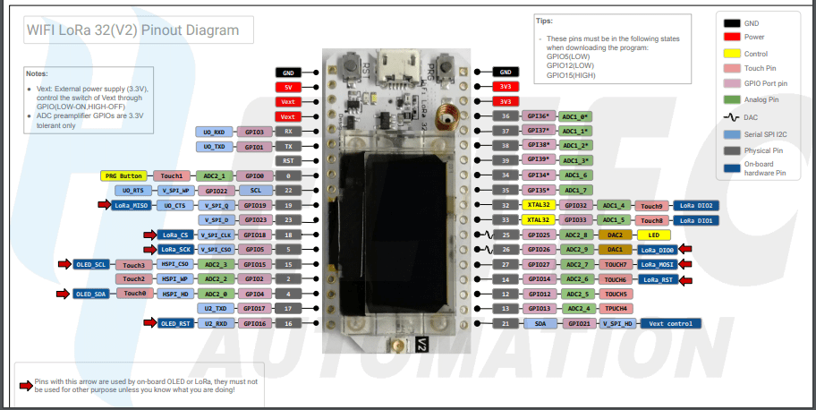
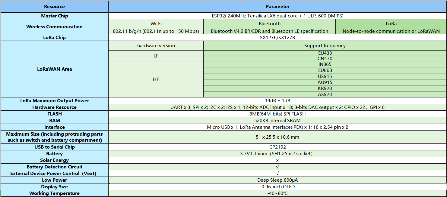
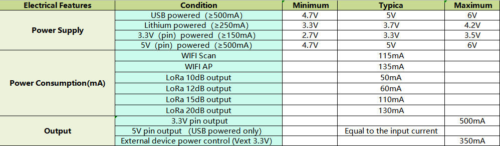
Heltec LoRa 32 v 2 – The good stuff ( according to me at least)
Technical SpecsElectrical SpecificationsPinout
Installation in Arduino IDE:
Installation of the libraries into the Arduino IDE is quite easy, just follow the link to heltec…
The Bad ( according to me )
The following module, is, according to me, an absolute waste of time and money. Documentation is impossible to find, and that that you do find, as often incorrect. The pin-outs are wrong, with no definite standard.
I am talking about the TTGO Lora V1 or V2 or what ever ??? can seem to even find that answer reliably. I was initially attracted to this module, as it was allegedly compatible with the heltec version, and did not have the oled screen, which, to be honest, is not always needed in every project. It was also about 25% cheaper, and could be sourced locally, without enriching the greedy shipping companies 😉 (I just have to rant about this, as 25USD to ship 100g worth of stuff is a ripoff. Either that or 60 to 90 days of guess-if-it-will-arrive mail is not on ( and even that is 10 USD!)
So, having high hopes, I ordered one of these boards, hoping to use it together with my heltec boards… It arrived, and that was well the top came of.. I could immediately see that the quality of the PCB was quite bad. Documentation was missing, and even the supplier sent me to a heltec pinout, which, after a quick test were definitely not correct…
Google turned up mixed results, and eventually I found a sort of accurate pinout …
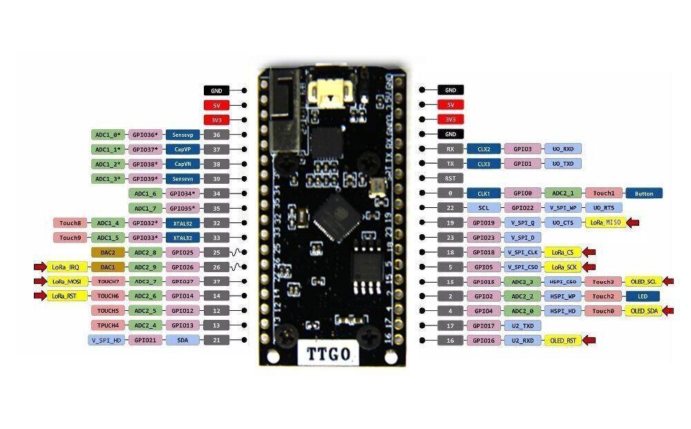
Alleged pinout for TTGO LoRa device
This pinout also turned out to be only about 50% correct, and after manually trying to map out the pins, I was sort of confident enough to test it further…
Further problems arose, LoRa does not work, I2C does not work, SPI does not work shall I continue…? 🙂 It now seems clear that the board that I bought was a clone of a clone, and a very bad one at that … I will post a picture of the actual board below, in the interest of education, to inform others not to get duped as well. Likewise, If I am the mistaken party, and you have had success with this board, please give me a message/yell and lets share some knowledge
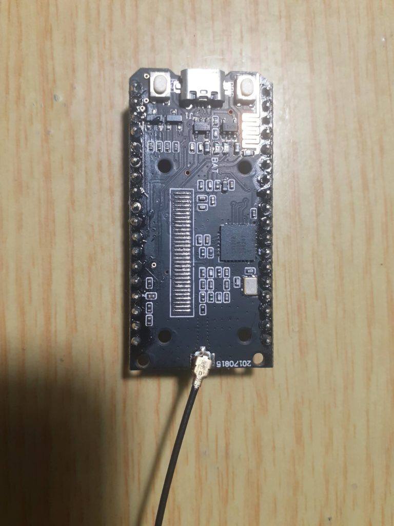
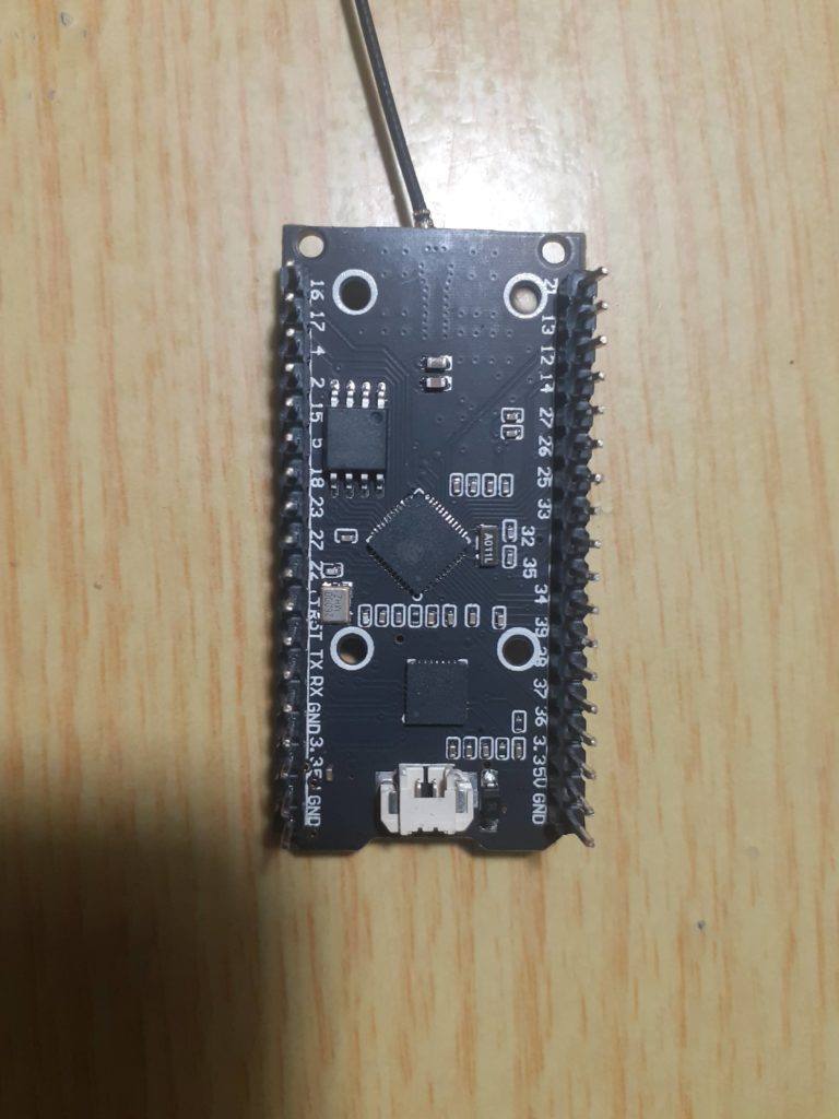
The Front (Top Side) of the Module
Front (Top) of the moduleBack (Bottom) of the module
I hope that you found this useful and that I will see you for part 3 of the series, where I will get into the actual coding.
When designing IoT solutions, we all encounter the problem of connecting our device(s) to each other, either directly, or through the internet. In Urban areas, it is quite easy to use WiFi or even GSM to achieve this, but these solutions often come with additional costs in the form of subscriptions. Although it is possible to run your own WiFi network free of charge, you will soon run into issues with the range…
Enter LoRa (short for Long Range) Radio communication. LoRa is a radio technology derived from chirp spread spectrum technology. It uses an ISM band, meaning it is unregulated in most countries, if you use the correct frequency for your country, that is.
It is also extremely low power, making it ideal for use with battery-powered devices. The technology is available in Node-to-Node, as well as Node-to -Gateway modes.
In this series, I will show you how to use a few of the existing LoRa Modules available on the market.
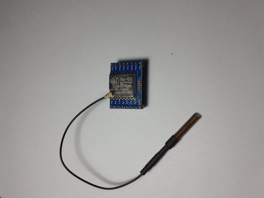
Ai-Tinker Ra-02 (Sx1278)
Ra-02 Lora Module, with spring antenna, by Ai-Tinker
This Module is conveniently broken-out onto a breakout board. It is sort of bread-board friendly (depending on the size of your bread-board) and is nicely labelled. It is also extremely cheap ( around $USD5 each, depending on where you buy from).
Caveats
There are quite a few important things that you should know about these modules before you start using them.
Disclaimer: The caveats listed below are by no means complete, or even valid. They are the result of experimentation by myself, with the intent to destroy a few modules, to see how hardy they are. Also take into mind, that living in SE Asia, it is quite common to buy something from a shop, where the seller has no or only a very limited idea of what he or she is selling, and are thus usually quite unable to provide any technical support.
To summarise: USE YOUR HEAD. If I did leave out something, it is quite possible that I forgot, or decided not to include it on purpose. This is a general guide, and you should ideally do your own research as well. That is the best way to learn.
1) Always connect an Antenna. This may seem like a logical one, but it is extremely important. The module is capable of quite a lot of transmission power, and operating it without an antenna will quickly damage the module, permanently.
2) ONLY use 3.3v, even on the control lines (the module uses SPI). This is quite important, as it is not very clearly stated by the suppliers, and will result in very short-lived component operation 😉 If you absolutely have to use 5v, use a level converter. (There are examples available on the internet, where they use this chip directly from an Arduino Uno. I can confirm that that approach does work, BUT, not for very long. I have purposely sacrificed a pair of transceiver modules so that you don’t have to. You can also adjust the SPI frequency, in the event that your level converter is not capable of running at a high SPI frequency.
3)Make sure that you connect ALL the ground pins on the device. This is another area that is not fully explained by the user manual and does “unexplainably” result in damaged modules.
4) Use short, good quality cables, and if possible, keep the module off the breadboard. While testing the modules, I found that the usual DuPont wires, as everyone should know by now, are quite unreliable. Combine that with a bread-board that has seen its share of use, and it is a definite recipe for headache 🙂
5) LoRa Antennas are polarised, make sure you have your antennas in the same orientation. Although this will not prevent it from working over short distances, it makes sense to just do it correctly. Good RF practices never hurt anybody 🙂
Connecting to Arduino
A Note on Power: It is important to power this module from a decent dedicated 3.3v power-supply. The Arduino Uno does sometimes have a 3.3v regulator on-board. From my tests, it is however not always up to the task, as the module may spike up to 120mA when transmitting. It is thus also recommended to have a nice fat capacitor across the power lines (decoupling cap) to soak up any spikes.
As mentioned above, a level converter is mandatory for a 5v Arduino. You may do without it if you use a 3.3v Arduino, but once again, your mileage will vary 🙂
Both the transmitter and receiver uses the same connections, which are listed below:
LoRa SX1278 Module
Arduino Board
3.3V
–
Gnd
Gnd
En/Nss
D10
G0/DIO0
D2
SCK
D13
MISO
D12
MOSI
D11
RST
D9
Connections to the Arduino from a LoRa RA-02 Module
Remember that you NEED a Level converter between the LoRa Module and the Arduino.
Software Library
The software library that we will use in our example is the excellent library from Sandeep Mistry. We will just include this into the Arduino IDE, and then use a slightly modified version of the examples for our experiment. It is also important to note that we will use Node-to Node communication, NOT LoRaWan. This means that all your communications will essentially be unencrypted, and not addressed. This does however allow you the flexibility to design and implement your own addressing scheme.
LORA code for Transmitting Side

#include <SPI.h>
#include <LoRa.h>

int counter = 0;

void setup() {
  Serial.begin(115200);
  while (!Serial);

  Serial.println("LoRa Sender");

  if (!LoRa.begin(433E6)) { // Set the frequency to that of your  //module. Mine uses 433Mhz, thus I have set it to 433E6
    Serial.println("Starting LoRa failed!");
    while (1);
  }

  LoRa.setTxPower(20);

}

void loop() {
  Serial.print("Sending packet: ");
  Serial.println(counter);

  // send packet
  LoRa.beginPacket();
  LoRa.print("hello ");
  LoRa.print(counter);
  LoRa.endPacket();

  counter++;

  delay(5000);
}
LORA code for Receiver Side

#include <SPI.h>
#include <LoRa.h>

void setup() {
  Serial.begin(115200);
  while (!Serial);

  Serial.println("LoRa Receiver");

  if (!LoRa.begin(433E6)) {
    Serial.println("Starting LoRa failed!");
    while (1);
  }
}

void loop() {
  // try to parse packet
  int packetSize = LoRa.parsePacket();
  if (packetSize) {
    // received a packet
    Serial.print("Received packet '");

    // read packet
    while (LoRa.available()) {
      Serial.print((char)LoRa.read());
    }

    // print RSSI of packet
    Serial.print("' with RSSI ");
    Serial.println(LoRa.packetRssi());
  }
}
Where to from here?
If all went well, you will see packets being received in the serial monitor of the Arduino IDE, connected to the receiver module. You will also see that the data from this example is sent as a string… It is however also possible to send binary data, by using the LoRa.write() function.
In the next part of this series, I will show you how to use LoRa with the ESP32/ESP8266, as well as a working example with binary data transmission and an addressing scheme in part 3.