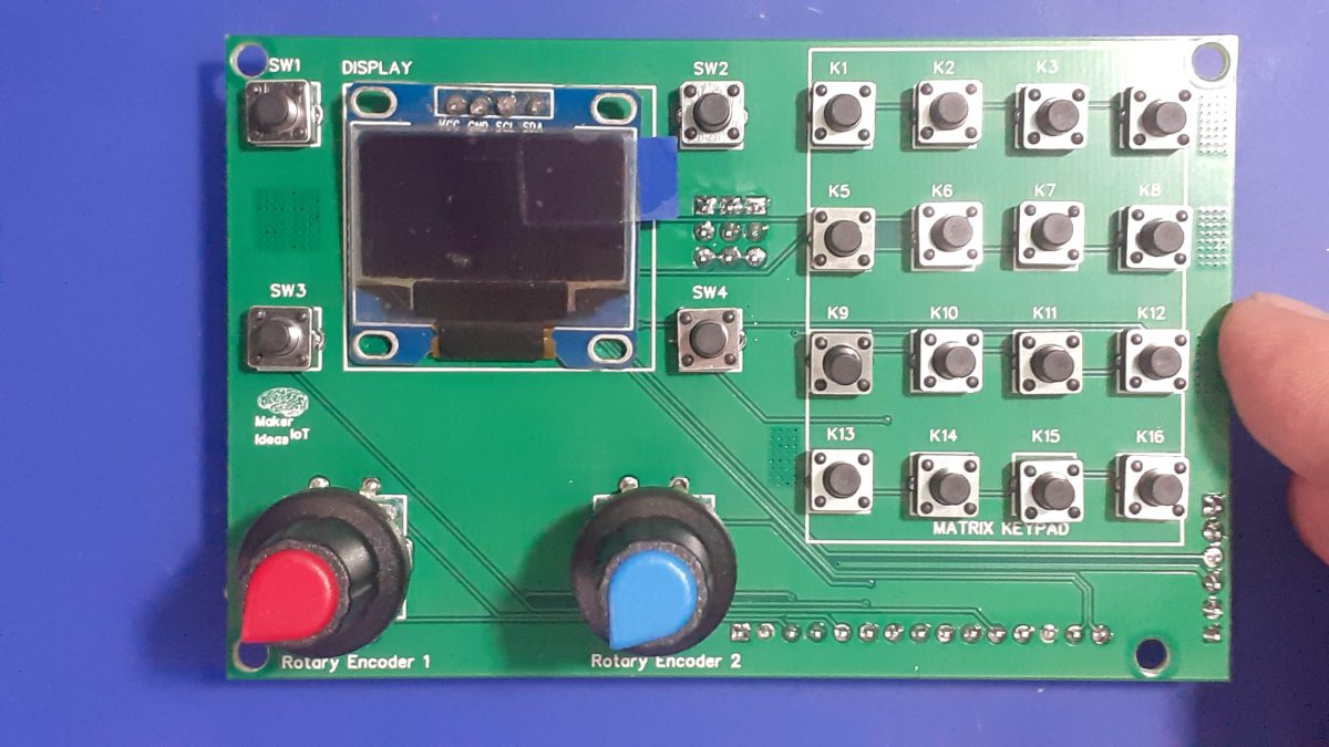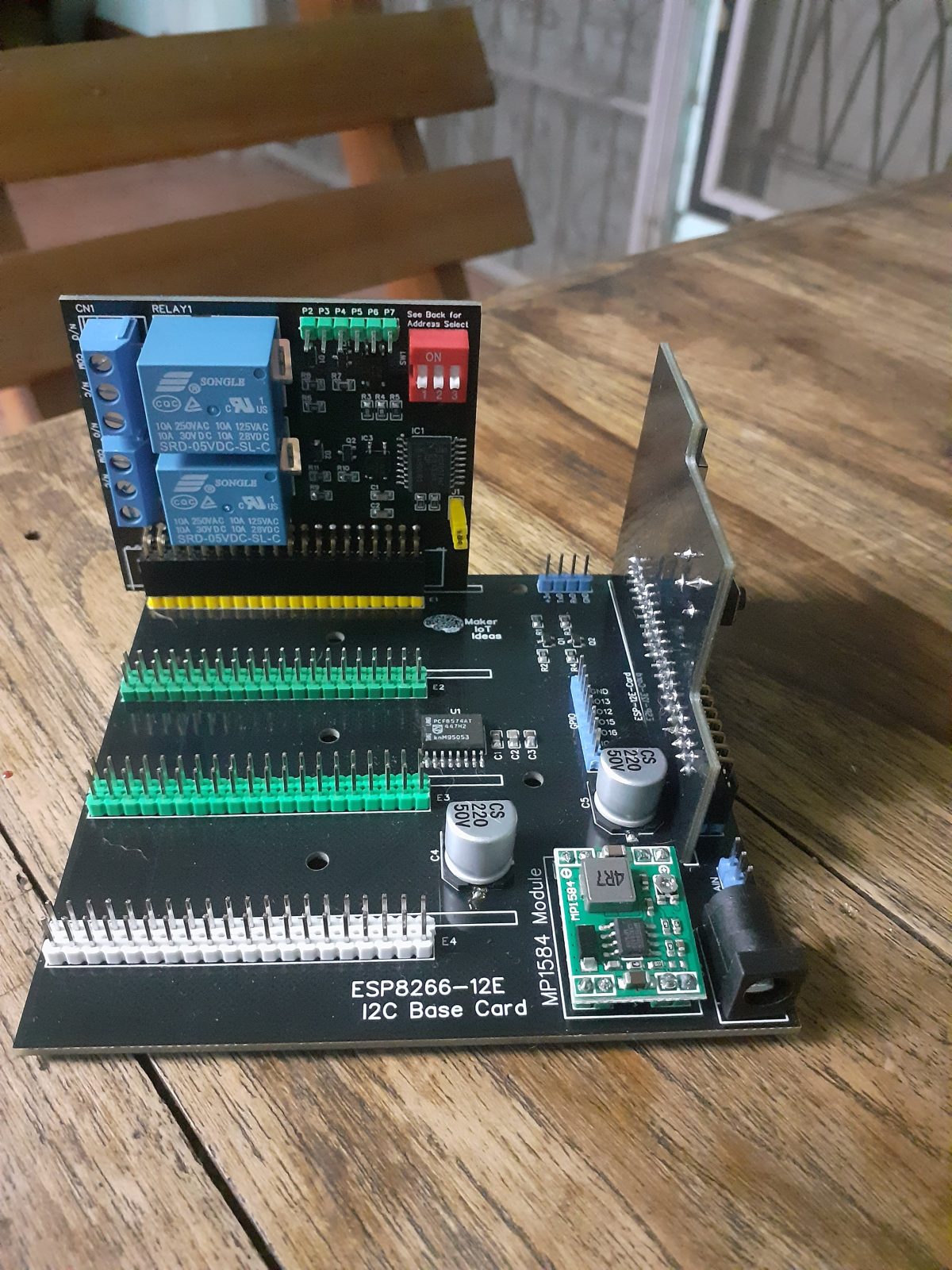
I designed this breakout to assist me during prototyping my next version of the “RP2040 Emergency Mouse“. In that project, I used the SEEED Studio Xiao RP2040, along with a few other components to create a simple but effective computer mouse-type device.
While the “mouse” works quite well, I have quite early on discovered that it could be better. More on that in a follow-up article, but let us just say that I needed more GPIO pins than that were available on the XIAO RP2040 and that the layout can be improved a bit – especially If I want to get it into an enclosure.
I am still quite neutral about CircuitPython and Micropython on microcontrollers, and Python in general, but since the above-mentioned project runs completely on CircuitPython, it made a lot of good sense to get more into it.
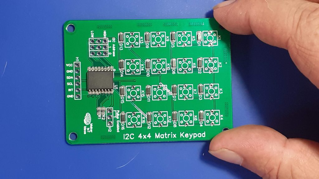
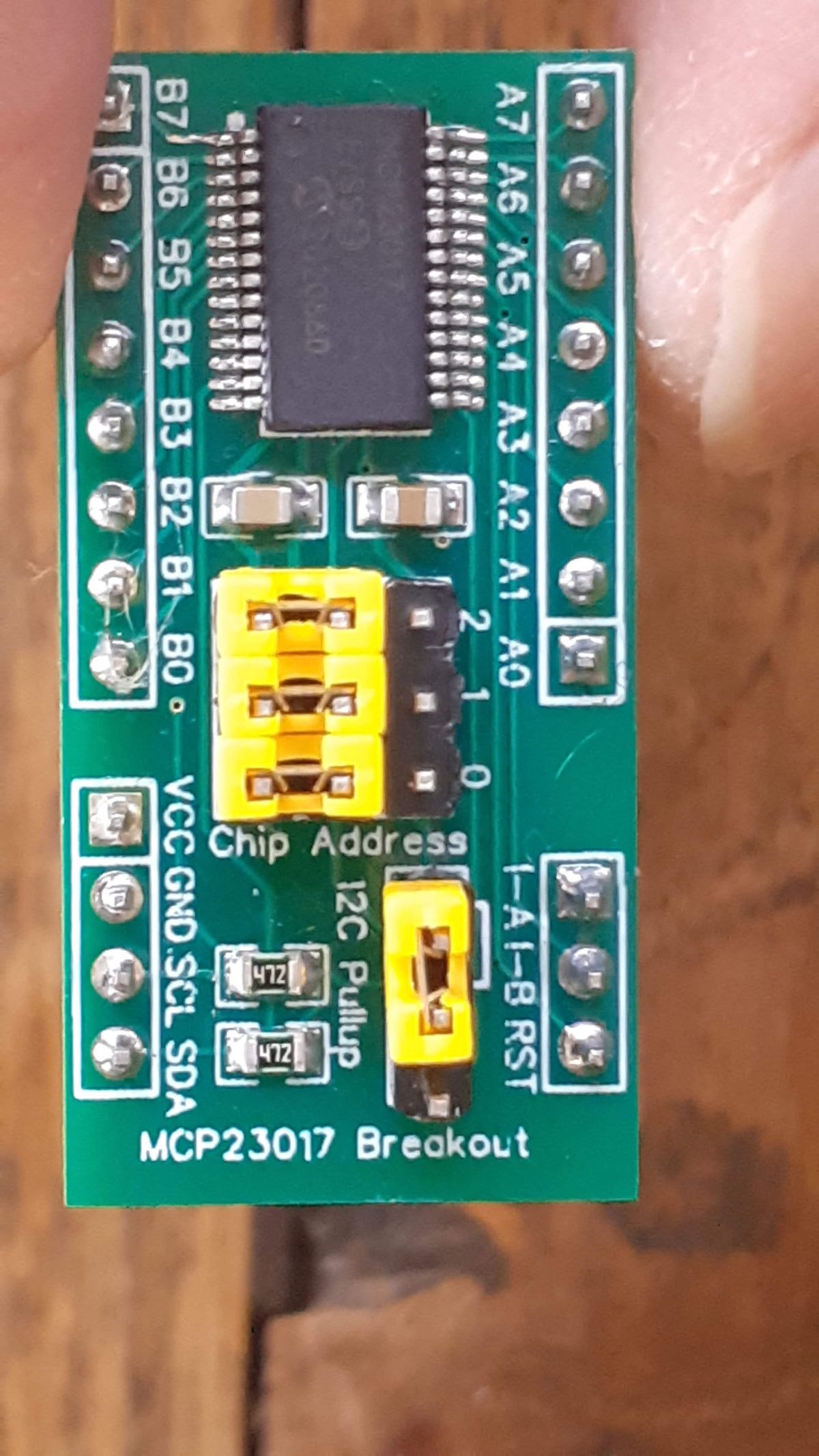
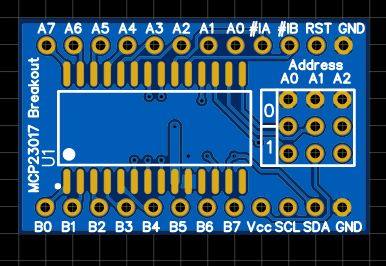
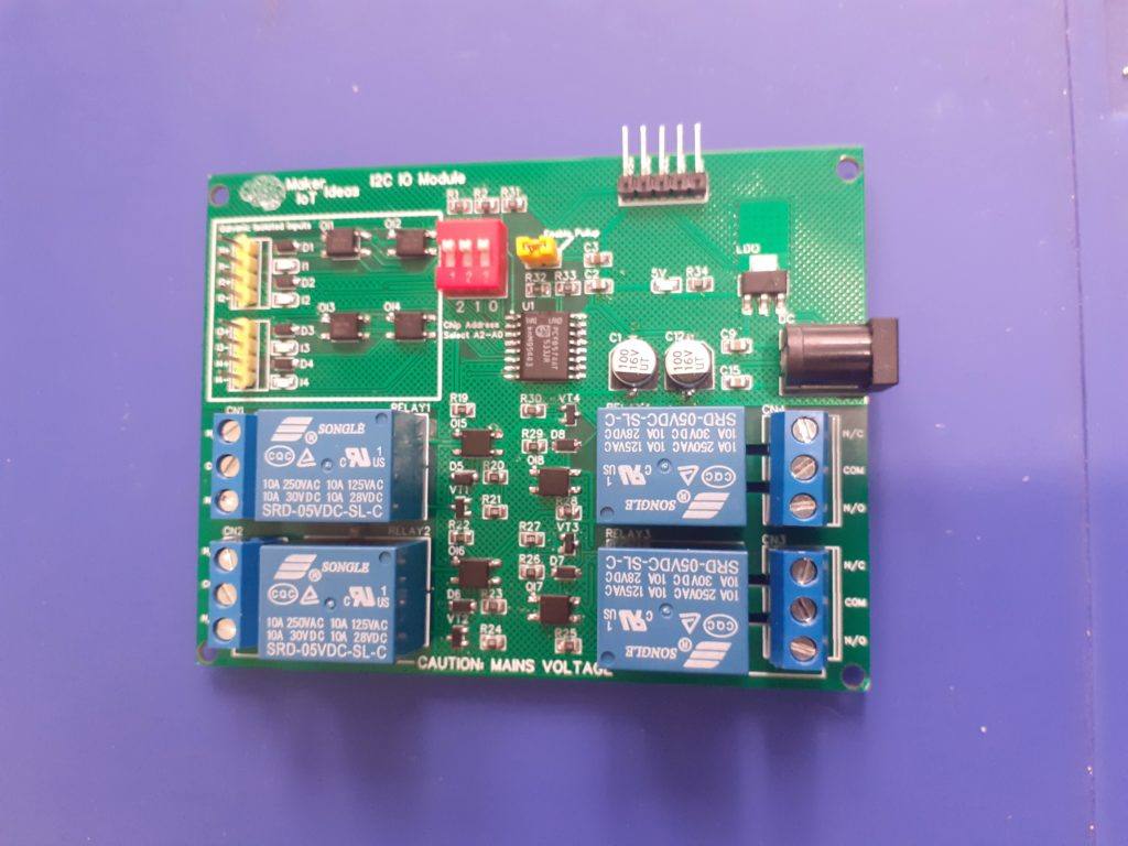
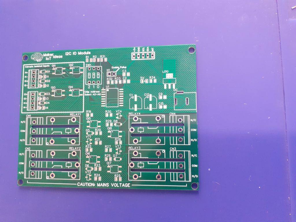
What is on the PCB?

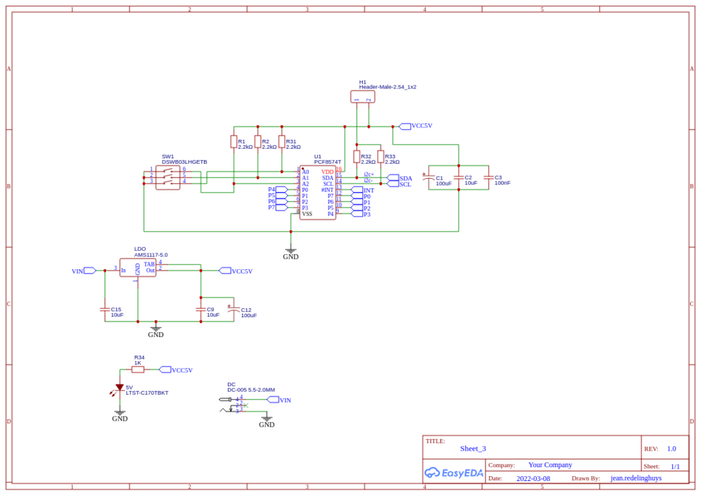
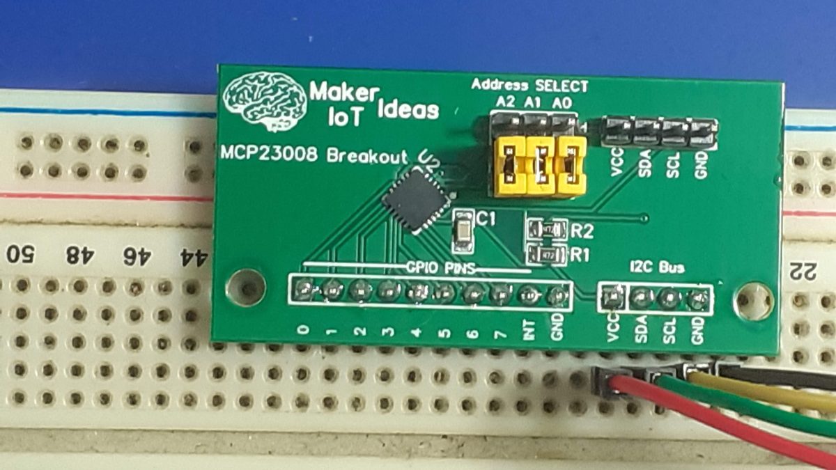
I wanted something as small as possible, and that meant that I chose a QFN package for the MCP23008 IO expander chip. At only 4mm x 4mm, and not being bothered to try and find a DIP version, a breakout board became a much-needed necessity.
Address Selection Jumpers, Two I2C bus headers, and of course the all-important GPIO pins make up all of the user accessible interfacing. Note that the chip reset line is permanently tied to Vcc to make things a bit less cluttered, and easier to use while prototyping.
A decoupling capacitor, as well as pullup resistors on the I2c lines, were also included. Another note here, I did not provide my usual selection jumper to disable these on this particular board.
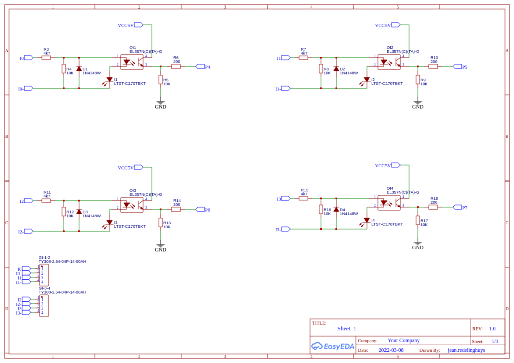
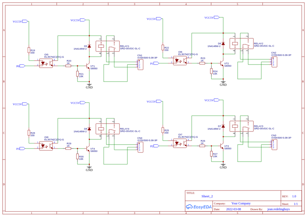
The Schematic

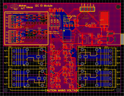
Manufacturing the PCB
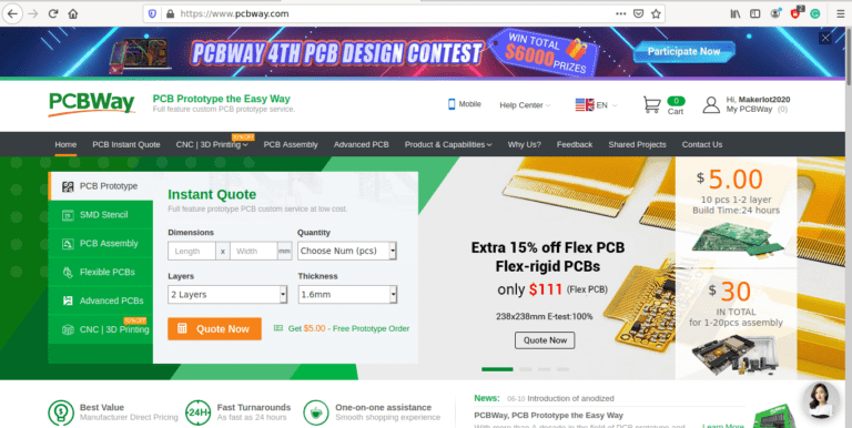
I choose PCBWay for my PCB manufacturing. Why? What makes them different from the rest?
PCBWay‘s business goal is to be the most professional PCB manufacturer for prototyping and low-volume production work in the world. With more than a decade in the business, they are committed to meeting the needs of their customers from different industries in terms of quality, delivery, cost-effectiveness and any other demanding requests. As one of the most experienced PCB manufacturers and SMT Assemblers in China, they pride themselves to be our (the Makers) best business partners, as well as good friends in every aspect of our PCB manufacturing needs. They strive to make our R&D work easy and hassle-free.
How do they do that?
PCBWay is NOT a broker. That means that they do all manufacturing and assembly themselves, cutting out all the middlemen, and saving us money.
PCBWay’s online quoting system gives a very detailed and accurate picture of all costs upfront, including components and assembly costs. This saves a lot of time and hassle.
PCBWay gives you one-on-one customer support, that answers you in 5 minutes ( from the Website chat ), or by email within a few hours ( from your personal account manager). Issues are really resolved very quickly, not that there are many anyway, but, as we are all human, it is nice to know that when a gremlin rears its head, you have someone to talk to that will do his/her best to resolve your issue as soon as possible.
Find out more here

Assembly and Testing
Due to the small size of the QFN package, I strongly recommend that you either have this assembled professionally, or at least consider buying a stencil for applying the solder paste to this board. Maybe those with excellent eyesight can do without that?

Assembly took only a few minutes, with the help of an extremely accurate stencil, followed by a few minutes on a hotplate, and manually soldering on the header pins.


Using the MCP23008 with CircuitPython
I2C devices are very easy to use with the Arduino IDE or similar, and as such, I will not be covering that here.
Circuitpython, however, is gaining popularity, and I am slowly starting to see what the hype is about myself…
So, to get started, you need a microcontroller running CircuitPython – See Adafruit for excellent tutorials. You will also need a few libraries from Adafruit
See this link
I will give a very simple example below, showing how to set a pin as an output, as well as an input with internal pullup resistors enabled. Note that the MCP23008 DOES NOT SUPPORT pull-down resistors internally. You need to add those by yourself externally.
# Initialising all the required libraries
import board
import busio
from digitalio import Direction
from adafruit_mcp230xx.mcp23008 import MCP23008
i2c = busio.I2C(board.SCL, board.SDA)
# Adding the MCP23008
mcp = MCP23008(i2c)
# This assumes that you are using the default address [ i.e. all address
# pins are grounded]
#
#
#
# Defining two outputs on pins 0 and 1
pin0 = mcp.get_pin(0)
pin0.direction = Direction.OUTPUT
pin1 = mcp.get_pin(1)
pin1.direction = Direction.OUTPUT
#
#
# We can now control the pins by setting them to true or false, true being
# high
pin0.value = True
pin1.value = True
#
# and switch them off again by using
pin0.value = False
pin1.value = False
#
#
# We can also use the pins as inputs.
# We will activate the internal pullup as well
#
# first , we need another library
import digitalio
pin2 = mcp.get_pin(2)
pin2.direction = digitalio.Direction.INPUT
pin2.pull = digitalio.Pull.UP
#
#
# Reading the pin value is now as easy as
pin2.value
#
# This will return True if the pin is high ( its default state with pullups # activated, of False if pulled low, by for example a switch of button )
Conclusion
The breakout works as expected, and it is very easy to use with CircuitPython.
I can now continue with the actual integration and Software for the RP2040 Mouse Rev 2.0 project.