
The electronics Breadboard is definitely one of those things that electronics hobbyists use quite a lot. It allows you to prototype your design relatively easily, with the use of breakout modules, wires and leaded components.
While this seems like a good thing, these breadboards are also unfortunately not perfect. The wires and connectors add electrical noise, and stray capacitance, as well as a certain level of unreliability.
My biggest issue with breadboards is not that though. it is the fact that you can only use through-hole components. Breakout PCBs is sort of a middle ground, as they allow you to connect SMD chips to stuff on a breadboard with wires, but that is not the issue here.
Doing a lot of prototyping, having a lot of components lying around, and then having to still try and find TH versions of everything to prototype with becomes costly in terms of time and space. If you have a larger project, but you are not yet at a stage to have a PCB made, adding another breadboard to the already cluttered setup is sometimes quite a challenge.
To get rid of this major point of frustration to me, I decided to try to solve it for myself by designing a SMD breadboard Hybrid.

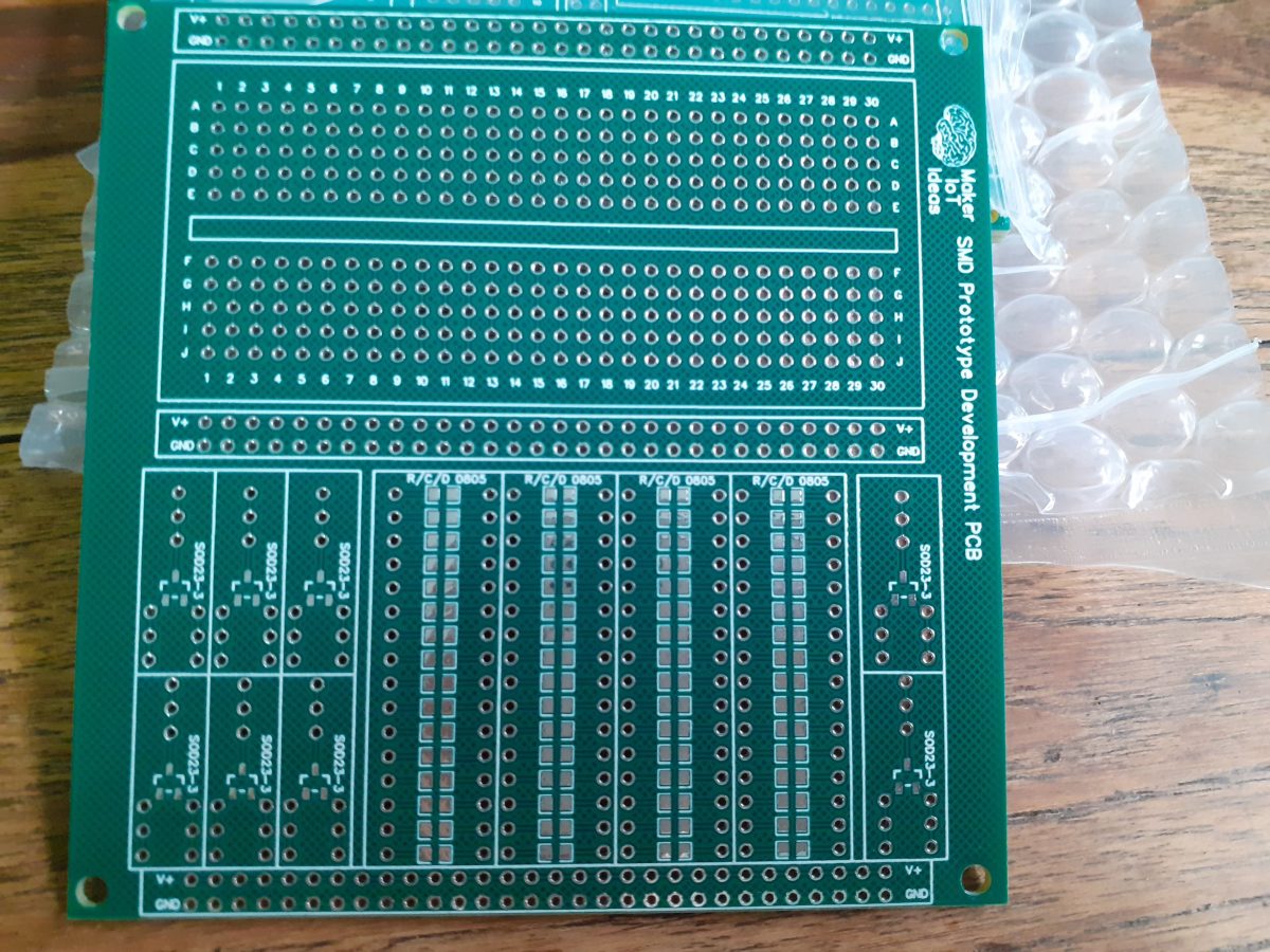
What is on the board?
Quick Specifications
-300-hole solderable breadboard (dual layer, plated through-hole pads)
-64 0805 SMD pads, with plated through hole pads for connectors
-8 BJT/Mosfet footprint pads (SOT233/SOD23-3) with 3 plated through-hole pads per terminal
– 3 Power rails, 30 holes each for Vcc and Ground (Common ground on all)
– Mesh-style ground plane on both sides of the PCB.
– 4 mounting holes
Details
To address all of the various issues that I have with breadboarding, I did the following:
I hardly ever use more than a 300-hole breadboard for single stage of a project.
Many of these circuit blocks could benefit from being a permanent soldered solution, but does not warrant the time and expense to design a dedicated PCB to hold them.
The first thing to do was thus to design a 300-hole PCB breadboard, complete with top and bottom power rails.
My next issue was SMD components. Chips have many footprints, and to try and design for each of them would turn into a nightmare. Breakout PCB’s would thus still be used for those. My biggest issue was BJT’s Mosfets Capacitors, diodes and resistors.
These can be bought in lead versions, but that was exactly what I tried to get away from, so it needed some thinking.
Resistors, capacitors and diodes have only two terminals, and could thus easily be soldered onto 0805 resistor pads (depending of course on the capacitor size )
BJTs and Mosfets need their own footprint.

Each of the SMD components has a corresponding through-hole pad, to easily connect it to a different part of the board as needed. BJT’s and Mosfets have 3 per leg.
Hopefully this will make things a bit more organised in future, and save me some time;
Manufacturing
Over the past eight years, PCBWay has continuously upgraded their MANUFACTURING plants and equipment to meet higher quality requirements, and now THEY also provide OEM services to build your products from ideas to mass production and access to the market.
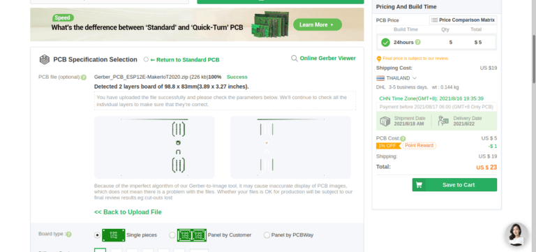
The PCB for this project has been manufactured at PCBWay.
Please consider supporting them if you would like your own copy of this PCB, or if you have any PCB of your own that you need to have manufactured.

If you would like to have PCBWAY manufacture one of your own, designs, or even this particular PCB, you need to do the following…
1) Click on this link
2) Create an account if you have not already got one of your own.
If you use the link above, you will also instantly receive a $5 USD coupon, which you can use on your first or any other order later. (Disclaimer: I will earn a small referral fee from PCBWay. This referral fee will not affect the cost of your order, nor will you pay any part thereof.)
3) Once you have gone to their website, and created an account, or login with your existing account,
4) Click on PCB Instant Quote

5) If you do not have any very special requirements for your PCB, click on Quick-order PCB

6) Click on Add Gerber File, and select your Gerber file(s) from your computer. Most of your PCB details will now be automatically selected, leaving you to only select the solder mask and silk-screen colour, as well as to remove the order number or not. You can of course fine-tune everything exactly as you want as well.

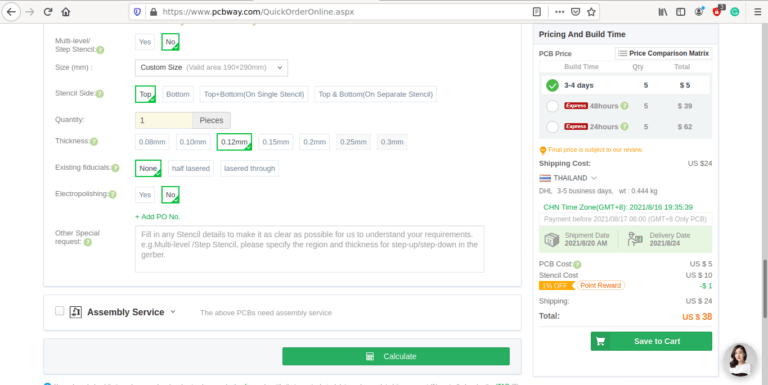
7) You can also select whether you want an SMD stencil, or have the board assembled after manufacturing. Please note that the assembly service, as well as the cost of your components, ARE NOT included in the initial quoted price. ( The quote will update depending on what options you select ).
8) When you are happy with the options that you have selected, you can click on the Save to Cart Button. From here on, you can go to the top of the screen, click on Cart, make any payment(s) or use any coupons that you have in your account.
Then just sit back and wait for your new PCB to be delivered to your door via the shipping company that you have selected during checkout.