I designed this breakout to assist me during prototyping my next version of the “RP2040 Emergency Mouse“. In that project, I used the SEEED Studio Xiao RP2040, along with a few other components to create a simple but effective computer mouse-type device.
While the “mouse” works quite well, I have quite early on discovered that it could be better. More on that in a follow-up article, but let us just say that I needed more GPIO pins than that were available on the XIAO RP2040 and that the layout can be improved a bit – especially If I want to get it into an enclosure.
I am still quite neutral about CircuitPython and Micropython on microcontrollers, and Python in general, but since the above-mentioned project runs completely on CircuitPython, it made a lot of good sense to get more into it.
What is on the PCB?
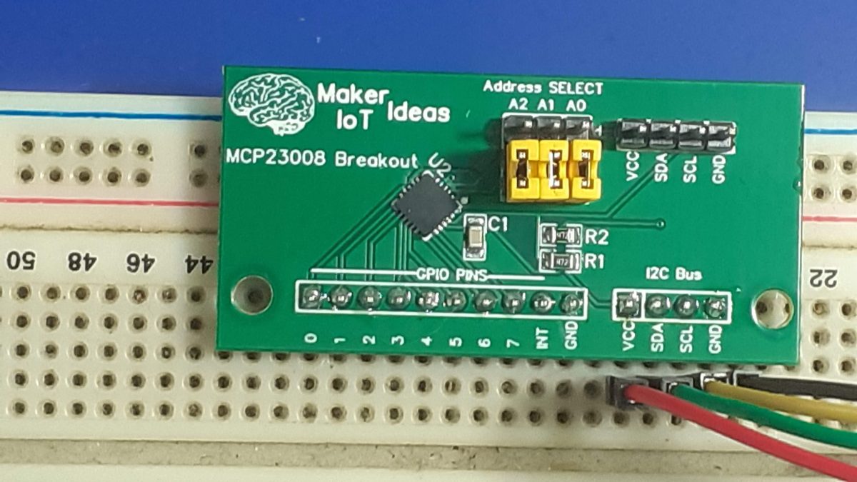
I wanted something as small as possible, and that meant that I chose a QFN package for the MCP23008 IO expander chip. At only 4mm x 4mm, and not being bothered to try and find a DIP version, a breakout board became a much-needed necessity.
Address Selection Jumpers, Two I2C bus headers, and of course the all-important GPIO pins make up all of the user accessible interfacing. Note that the chip reset line is permanently tied to Vcc to make things a bit less cluttered, and easier to use while prototyping.
A decoupling capacitor, as well as pullup resistors on the I2c lines, were also included. Another note here, I did not provide my usual selection jumper to disable these on this particular board.
The Schematic
Manufacturing the PCB
I choose PCBWay for my PCB manufacturing. Why? What makes them different from the rest?
PCBWay‘s business goal is to be the most professional PCB manufacturer for prototyping and low-volume production work in the world. With more than a decade in the business, they are committed to meeting the needs of their customers from different industries in terms of quality, delivery, cost-effectiveness and any other demanding requests. As one of the most experienced PCB manufacturers and SMT Assemblers in China, they pride themselves to be our (the Makers) best business partners, as well as good friends in every aspect of our PCB manufacturing needs. They strive to make our R&D work easy and hassle-free.
How do they do that?
PCBWay is NOT a broker. That means that they do all manufacturing and assembly themselves, cutting out all the middlemen, and saving us money.
PCBWay’s online quoting system gives a very detailed and accurate picture of all costs upfront, including components and assembly costs. This saves a lot of time and hassle.
PCBWay gives you one-on-one customer support, that answers you in 5 minutes ( from the Website chat ), or by email within a few hours ( from your personal account manager). Issues are really resolved very quickly, not that there are many anyway, but, as we are all human, it is nice to know that when a gremlin rears its head, you have someone to talk to that will do his/her best to resolve your issue as soon as possible.
Due to the small size of the QFN package, I strongly recommend that you either have this assembled professionally, or at least consider buying a stencil for applying the solder paste to this board. Maybe those with excellent eyesight can do without that?
Assembly took only a few minutes, with the help of an extremely accurate stencil, followed by a few minutes on a hotplate, and manually soldering on the header pins.
Using the MCP23008 with CircuitPython
I2C devices are very easy to use with the Arduino IDE or similar, and as such, I will not be covering that here.
Circuitpython, however, is gaining popularity, and I am slowly starting to see what the hype is about myself…
So, to get started, you need a microcontroller running CircuitPython – See Adafruit for excellent tutorials. You will also need a few libraries from Adafruit See this link
I will give a very simple example below, showing how to set a pin as an output, as well as an input with internal pullup resistors enabled. Note that the MCP23008 DOES NOT SUPPORT pull-down resistors internally. You need to add those by yourself externally.
# Initialising all the required libraries
import board
import busio
from digitalio import Direction
from adafruit_mcp230xx.mcp23008 import MCP23008
i2c = busio.I2C(board.SCL, board.SDA)
# Adding the MCP23008
mcp = MCP23008(i2c)
# This assumes that you are using the default address [ i.e. all address
# pins are grounded]
#
#
#
# Defining two outputs on pins 0 and 1
pin0 = mcp.get_pin(0)
pin0.direction = Direction.OUTPUT
pin1 = mcp.get_pin(1)
pin1.direction = Direction.OUTPUT
#
#
# We can now control the pins by setting them to true or false, true being
# high
pin0.value = True
pin1.value = True
#
# and switch them off again by using
pin0.value = False
pin1.value = False
#
#
# We can also use the pins as inputs.
# We will activate the internal pullup as well
#
# first , we need another library
import digitalio
pin2 = mcp.get_pin(2)
pin2.direction = digitalio.Direction.INPUT
pin2.pull = digitalio.Pull.UP
#
#
# Reading the pin value is now as easy as
pin2.value
#
# This will return True if the pin is high ( its default state with pullups # activated, of False if pulled low, by for example a switch of button )
Conclusion
The breakout works as expected, and it is very easy to use with CircuitPython. I can now continue with the actual integration and Software for the RP2040 Mouse Rev 2.0 project.
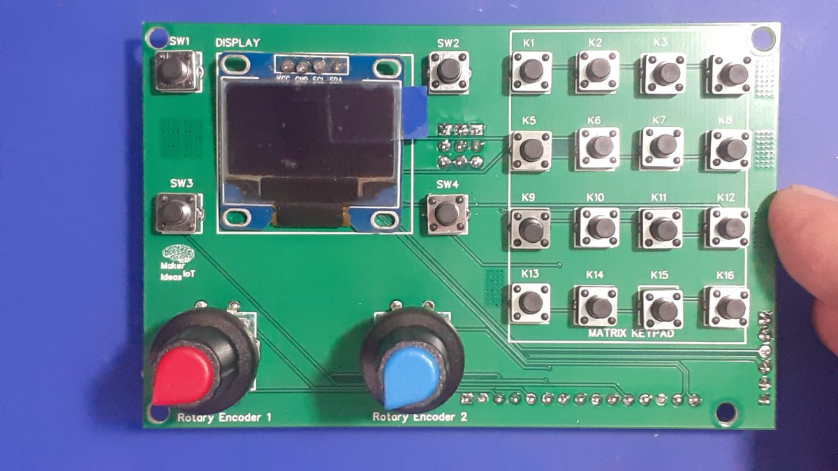
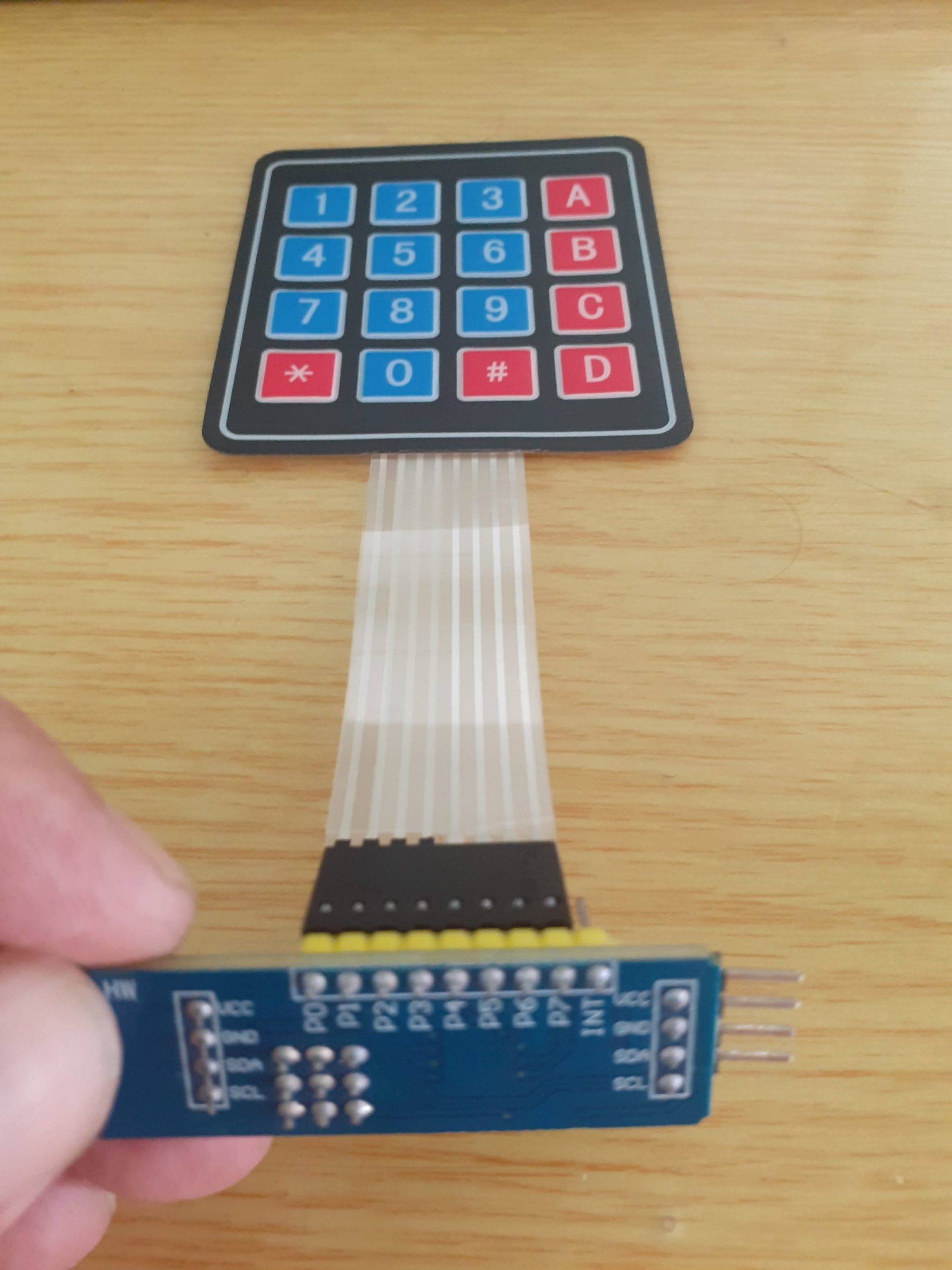
When we are working on a prototype, we always need access to pushbuttons, encoders and even displays to test our ideas in the real world. This Multi-Purpose IO Card was designed to help me do just that…
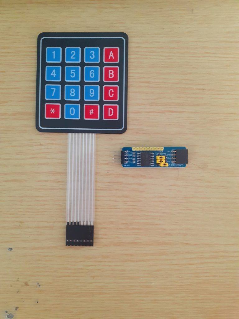
What is on the PCB?
This PCB was designed with my particular work style in mind. I use a lot of I2C devices, IO Expanders, Displays and sensors. It would thus make sense to have I2C on the PCB, to control an OLED display, as well as a PCF8574 IO expander, that is used to drive a 4×4 Matrix Keypad. Two Rotary encoders, as well as another 4 standard push buttons completes the PCB…
The features, summarised is as follows:
1x Matrix Keypad (4×4) Controlled via an PCF8574 IO expander with selectable addressing. 1x SSD1306 OLED I2C Display 4x Momentary pushbuttons, configured to be used with internal pullups – i.e pushing the button pulls the GPIO LOW 2x Rotary Encoders, with integrated Pushbutton, also configured as Active LOW
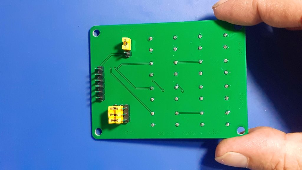
The board has all of the connectors and jumpers on the back, making it possible to mount it to an enclosure as a control panel.
I have also provided an additional I2C header to make it possible to add additional devices to the I2C bus easily
The PCB in Detail
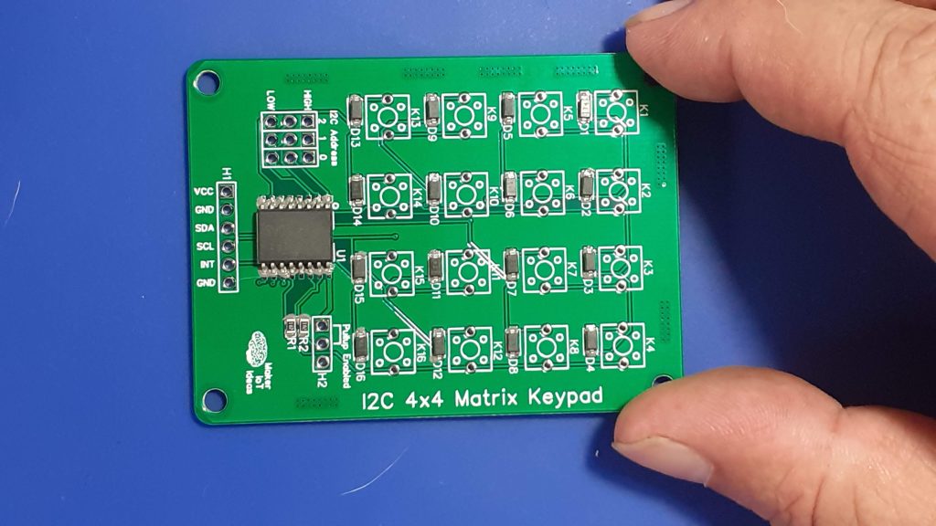
PCB Top
Starting from left to right, we have two push-buttons, an OLED display, with two rotary encoders below the display, and another two momentary push buttons. On the Right, we have a 4×4 matrix keypad, and various pin headers for connection to a microcontroller of your choice.
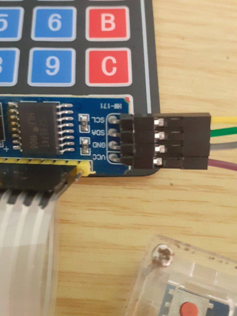
On the back, we have the PCF8574 IO expander for the Matric keypad, addressing Jumpers for the IO expander, as well as the two pin headers for connections to and from a microcontroller…
The Pinouts of these are as follows: Horizontal 15 pin 2.54mm connector SDA I2C Data SCA I2C Clock
RE2-D Rotary Encoder 2 Push Button RE2-B Rotary Encoder 2 Pin B RE2-A Rotary Encoder 2 Pin A
RE1-D Rotary Encoder 1 Push Button RE1-B Rotary Encoder 1 Pin B RE1-A Rotary Encoder 1 Pin A
GND VCC 3.3v to 5v DC
The Expansion header extends the I2C Bus, as well as proved access to the interrupt pin on the PCF8574. VCC and GND are also provided.
The Schematic
Manufacturing the PCB
I choose PCBWay for my PCB manufacturing. Why? What makes them different from the rest?
PCBWay‘s business goal is to be the most professional PCB manufacturer for prototyping and low-volume production work in the world. With more than a decade in the business, they are committed to meeting the needs of their customers from different industries in terms of quality, delivery, cost-effectiveness and any other demanding requests. As one of the most experienced PCB manufacturers and SMT Assemblers in China, they pride themselves to be our (the Makers) best business partners, as well as good friends in every aspect of our PCB manufacturing needs. They strive to make our R&D work easy and hassle-free.
How do they do that?
PCBWay is NOT a broker. That means that they do all manufacturing and assembly themselves, cutting out all the middlemen, and saving us money.
PCBWay’s online quoting system gives a very detailed and accurate picture of all costs upfront, including components and assembly costs. This saves a lot of time and hassle.
PCBWay gives you one-on-one customer support, that answers you in 5 minutes ( from the Website chat ), or by email within a few hours ( from your personal account manager). Issues are really resolved very quickly, not that there are many anyway, but, as we are all human, it is nice to know that when a gremlin rears its head, you have someone to talk to that will do his/her best to resolve your issue as soon as possible.
The assembly of this PCB was relatively easy, as it contains only a single SMD component. I do however have to alert you to a certain caveat…
On the PCB, the I2C OLED display pinout is, from left to right,
VCC GND SDC SDA
I have however come across similar displays that swap the GND and VCC pins… and some that even have SCL and SDA swapped…
It is thus quite important that you check your display BEFORE soldering it to this PCB…
Addressing the PCF8574 is also quite easy, with the jumper towards the top is a high, and towards the bottom is a low… They are marked A2 A1 A0 and thus, counting in binary, all low will be 0x20h and all high will be ox27h
Also, note that there are NO I2C Pullup resistors on the board. My microcontroller PCB’s usually have these already, and most I2C Sensors, including the OLED Display that we use, already include as well… You should thus check what you have on your own hardware, as it is quite impossible to cater for every situation… In a future version, I may add selectable pullup resistors onto this board as well…
Coding and Firmware
The possible uses of this board is quite broad, and the code possibilities are thus also quite extensive. Since I mainly use ESPHome or the Arduino IDE with most of my projects, I wont be including any specialised code here. I think it is enough to say that almost all of the available PCF8574 Matrix Keypad libraries available for the Arduino IDE will fork with this board…
The pinouts are important, and thus :
Row 0 – P0 Row 1 – P1 Row 2 – P2 Row 4 – P3
Col 0 – P7 Col 1 – P6 Col 2 – P5 Col 3 – P4
As far as ESPHome goes, you will need to 1) Add an I2c bus for your device 2)Add a PCF8574 component 3)Add a Matrix Keypad component, and refer the rows and columns to the pins on the PCF8574 – See below for an example of how I have done that in a previous project.
#I2C bus

i2c:

sda: 4

scl: 5

scan: true

id: I2C_Bus

#
# In my case, SDA is on GPIO4 and SCL is on GPIO5
# This is similar to the standard configuration on a NodeMCU v2 Dev board
#

#
# The next step is to configure the actual IO Expander, which in my case is located
# at address 0x27
#

#PCF8574

pcf8574:

- id: 'pcf8574_hub'

address: 0x27

pcf8575: false


#
# Now we can add the actual keypad interface to the YAML file
# Take note of the difference from the ESP32 file above.
#
#

#KEYPAD

matrix_keypad:

id: mykeypad

rows:

- pin:

pcf8574: pcf8574_hub

# Use pin number 0

number: 0

# In the ESP32 file, we wHereould specify a pin directly like:
#
# -pin: 17
#
# That approach will not work for us.
# The reason for that is that we have to redirect the GPIO to a
# physical pin on the PCF8574 IO expander.
#
# That is done with the following syntax
#
# - pin:
#pcf8574: pcf8574_hub -- This is the ID of the PCF8574 device -
#number: 0 -- The actual pin number

- pin:

pcf8574: pcf8574_hub

# Use pin number 0

number: 1

- pin:

pcf8574: pcf8574_hub

# Use pin number 0

number: 2

- pin:

pcf8574: pcf8574_hub

# Use pin number 0

number: 3

columns:

- pin:

pcf8574: pcf8574_hub

# Use pin number 0

number: 7

- pin:

pcf8574: pcf8574_hub

# Use pin number 0

number: 6

- pin:

pcf8574: pcf8574_hub

# Use pin number 0

number: 5

- pin:

pcf8574: pcf8574_hub

# Use pin number 0

number: 4

keys: "123A456B789C*0#D"

has_diodes: false
The Rotary encoders and momentary push-buttons can be handled in the same manner, using standard libraries in the Arduino IDE, or a rotary encoder component in ESPHome…
The OLED display would also be handled as above, with a DISPLAY component in ESPHome…
Summary and next steps
The next steps, for me at least, would be to design and CNC cut a suitable enclosure for the IO panel/Control panel in order to make it easier to use…
The panel was designed to be a tool to aid me while designing, and part of my never-ending battle getting rid of breadboards.
It does its job well, at least so far, and works as I have intended it to.
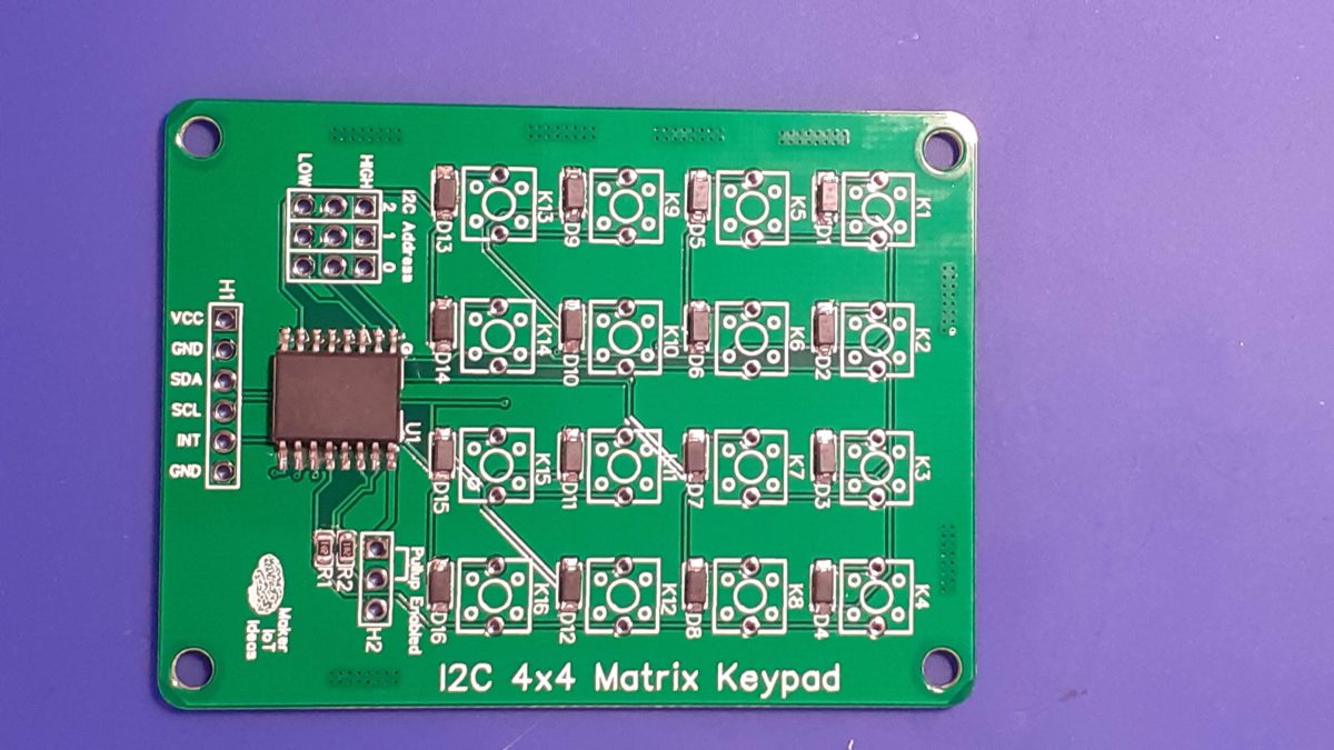
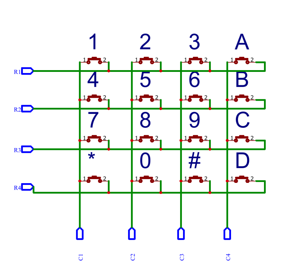
In a previous post this month I introduced my 4×4 matrix keypad. That keypad was designed to be directly interfaced to a microcontroller’s GPIO pins or alternatively to an IO expander chip like the PCF8574. That design, while working very well had the problem of requiring 8 GPIO pins to function correctly.
GPIO pins on a microcontroller can be considered very precious resources, and it should then be logical to assume that we should find a way to use these GPIO pins in a more conservative way, to allow us to interface more peripherals.
I solved this problem by integrating the keypad with an IO Expander on the same PCB. That will allow us to get away with using only 2 GPIO pins, and also open up the option of adding more keypads to the I2C bus, in the event that we need that many keys for a particular project.
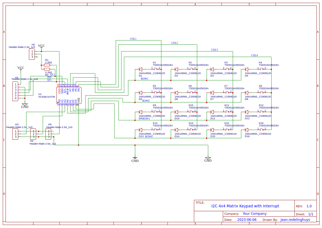
The Schematic
I2C 4×4 Matrix Keypad Schematic
Looking closely at the schematic, we can see that it is exactly the same basic keypad circuit that I used in the initial design. The only difference is that in this design, I have integrated a PCF8574 directly onto the PCB.
Some additional features include selectable I2C Pullup resistors ( usually my microcontroller development boards already include those) that can be activated with a jumper when needed. There are also a set of address selection jumpers, making it possible to stack keypads together into a bigger keyboard if you require something like that. Note that, in this version of the hardware, I did not include headers for stacking.
The keypad can be powered by a DC power source of 3.3v to 5v.
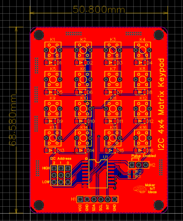
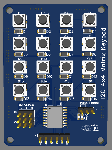
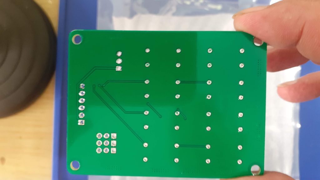
The PCB
I2C Keypad PCB
3D Render of the I2C Keypad
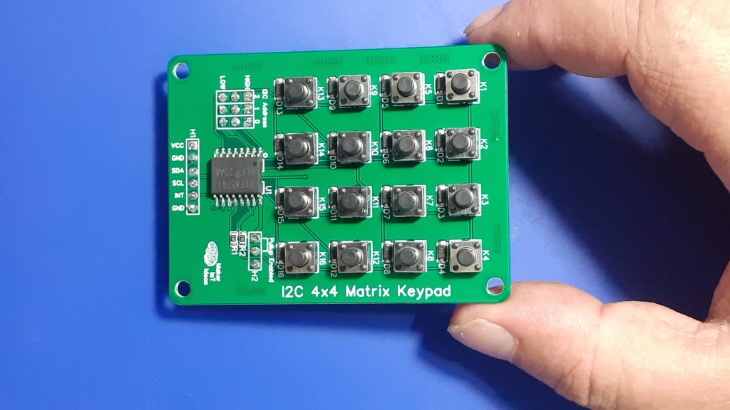
The PCB is a double-layer board of 68.8mm x 50.8mm. Male header pins provide access to the connections as well as address and pullup resistor jumpers. In my build, I have mounted these male headers on the back of the PCB. That makes it possible to mount the Keypad in an enclosure without having the jumpers “stick out” and get in the way.
The top layer of the I2C Keypad PCBBottom Layer
Manufacturing
I choose PCBWay for my PCB manufacturing. This month, PCBWay is also celebrating its 9th anniversary, and that means that there are quite a lot of very special offers available.
Why? What makes them different from the rest?
PCBWay‘s business goal is to be the most professional PCB manufacturer for prototyping and low-volume production work in the world. With more than a decade in the business, they are committed to meeting the needs of their customers from different industries in terms of quality, delivery, cost-effectiveness and any other demanding requests. As one of the most experienced PCB manufacturers and SMT Assemblers in China, they pride themselves to be our (the Makers) best business partners, as well as good friends in every aspect of our PCB manufacturing needs. They strive to make our R&D work easy and hassle-free.
How do they do that?
PCBWay is NOT a broker. That means that they do all manufacturing and assembly themselves, cutting out all the middlemen, and saving us money.
PCBWay’s online quoting system gives a very detailed and accurate picture of all costs upfront, including components and assembly costs. This saves a lot of time and hassle.
PCBWay gives you one-on-one customer support, that answers you in 5 minutes ( from the Website chat ), or by email within a few hours ( from your personal account manager). Issues are really resolved very quickly, not that there are many anyway, but, as we are all human, it is nice to know that when a gremlin rears its head, you have someone to talk to that will do his/her best to resolve your issue as soon as possible.
The assembly of this PCB was quite easy and quick. A stencil is not required. All SMD components are 0805 or bigger. It would thus be quite easy to solder them all by hand with a fine-tipped soldering iron.
I have however used soldering paste and hot air to reflow the components, as it is the fastest, in my opinion, and definitely looks neater than hand soldering.
After placing SMD components onto solder paste – ready for reflow solderingAfter Reflow soldering with Hot Air
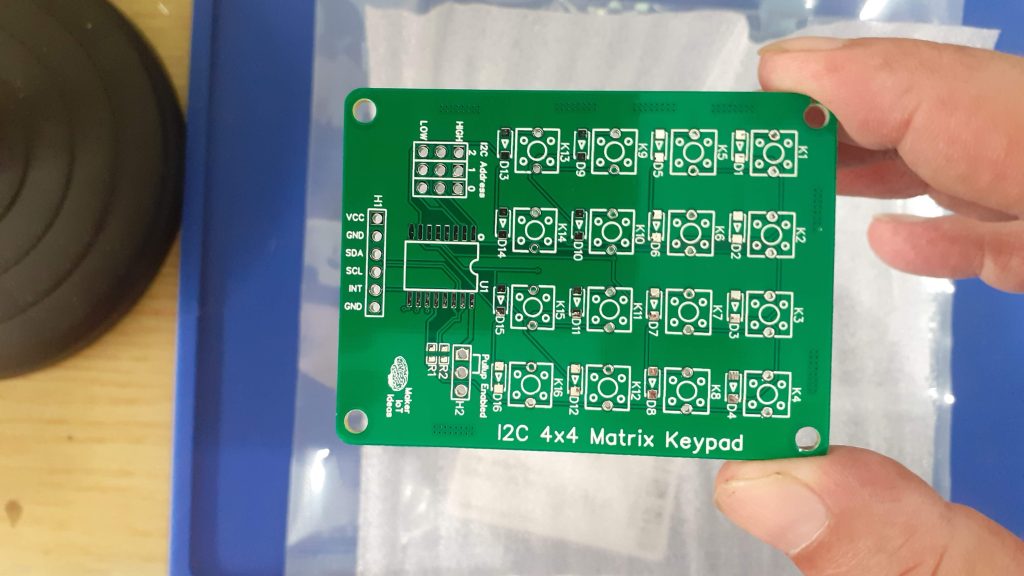
The board is now ready to solder the switches and header pins in place. As already mentioned above, I chose to assemble the headers on the back of the PCB to prevent them from interfering with any enclosure that I may later use with the keypad.
Final AssemblyNote that I assembled the headers onto the back of the PCB.
Testing and Coding
Testing the keypad consisted of a few steps, the first of which was ensuring that there were no short circuits, as well as that all the momentary switches worked. This was done with a multimeter in continuity as well as diode mode, with probes alternatively on each column and row in turn, while pressing the buttons.
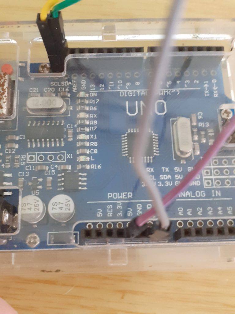
The next stage was testing the I2C IO Expander. This was done with a simple I2C Scanning sketch on an Arduino Uno. It did not do a lot, but, I could see that the PCF8574 is responding to its address and that the pullup resistors work when enabled. This test was repeated with my own ESP8266 and ESP32 boards, this time with pullup resistors disabled, as these boards already have them onboard.
Coding came next, and it was another case of perspectives. It seems like all commercial keypads do not have diodes. This affects the way that they work with a given library. It seems that software developers and hardware developers have different understandings of what a row and a column is.
This meant that, due to the fact that I have diodes on each switch, and the way that the library work – which pins are pulled high and which are set as inputs -, I had to swap around my rows and columns in the software to get everything to work. On a keypad with the diodes replaced with 0-ohm links, that was not needed.
A short test sketch follows below:
Note that with was run on an ESP8266-12E, therefore the Wire.begin() function was changed to Wire.begin(4,5); in order to use GPIO 4 and GPIO 5 for I2C
Another point to note is that the keypad Layout will seem strange. Remember that this is due to the diodes in series on each switch. That forces us to swap around the Rows and the Columns in the software, resulting in a mirrored and rotated left representation of the keypad. It looks funny, but believe me, it actually still works perfectly.
#include <Wire.h>
#include "Keypad.h"
#include <Keypad_I2C.h>

const byte n_rows = 4;
const byte n_cols = 4;

char keys[n_rows][n_cols] = {
    {'1', '4', '7', '*'},
    {'2', '5', '8', '0'},
    {'3', '6', '9', '#'},
    {'A', 'B', 'C', 'D'}};

byte rowPins[n_rows] = {4, 5, 6, 7};
byte colPins[n_cols] = {0, 1, 2, 3};

Keypad_I2C myKeypad = Keypad_I2C(makeKeymap(keys), rowPins, colPins, n_rows, n_cols, 0x20);

String swOnState(KeyState kpadState)
{
    switch (kpadState)
    {
    case IDLE:
        return "IDLE";
        break;
    case PRESSED:
        return "PRESSED";
        break;
    case HOLD:
        return "HOLD";
        break;
    case RELEASED:
        return "RELEASED";
        break;
    } // end switch-case
    return "";
} // end switch on state function

void setup()
{
    // This will be called by App.setup()
    Serial.begin(115200);
    while (!Serial)
    { /*wait*/
    }
    Serial.println("Press any key...");
    Wire.begin(4,5);
    myKeypad.begin(makeKeymap(keys));
}

char myKeyp = NO_KEY;
KeyState myKSp = IDLE;
auto myHold = false;

void loop()
{

    char myKey = myKeypad.getKey();
    KeyState myKS = myKeypad.getState();

    if (myKSp != myKS && myKS != IDLE)
    {
        Serial.print("myKS: ");
        Serial.println(swOnState(myKS));
        myKSp = myKS;
        if (myKey != NULL)
            myKeyp = myKey;
        String r;
        r = myKeyp;
        Serial.println("myKey: " + String(r));
        if (myKS == HOLD)
            myHold = true;
        if (myKS == RELEASED)
        {
            if (myHold)
                r = r + "+";
            Serial.println(r.c_str());
            myHold = false;
        }
        Serial.println(swOnState(myKS));
        myKey == NULL;
        myKS = IDLE;
    }
}
Conclusion
This project once again delivered what I set out to achieve. It has some quirks, but nothing serious. Everything works as expected, both in the Arduino IDE/platform IO realm, as well as in ESPHome. It is worth noting that in ESPHome, we do not need to swap the rows and columns to use the Keypad component. Do remember to leave the has_diodes flag to false though…
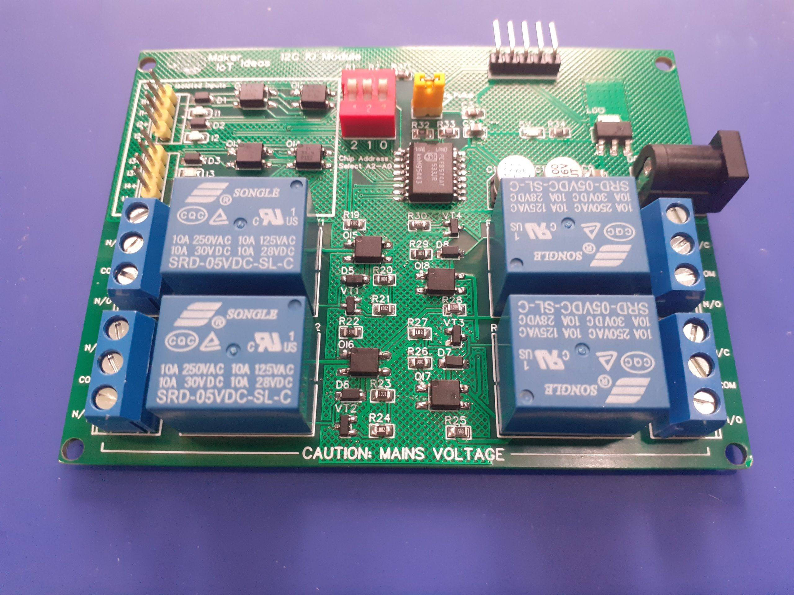
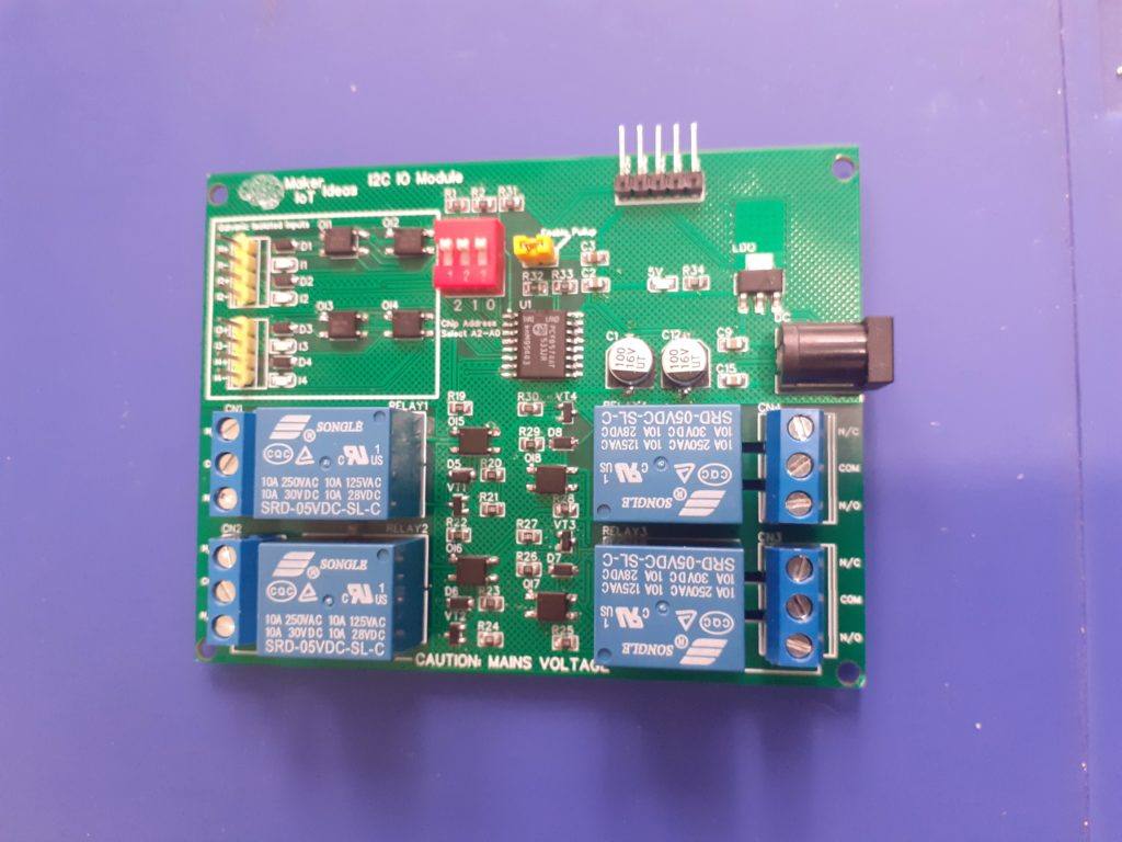
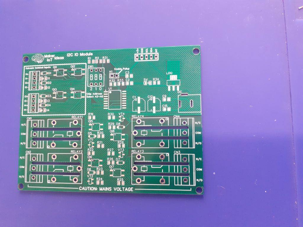
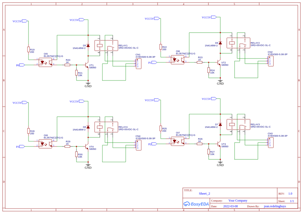
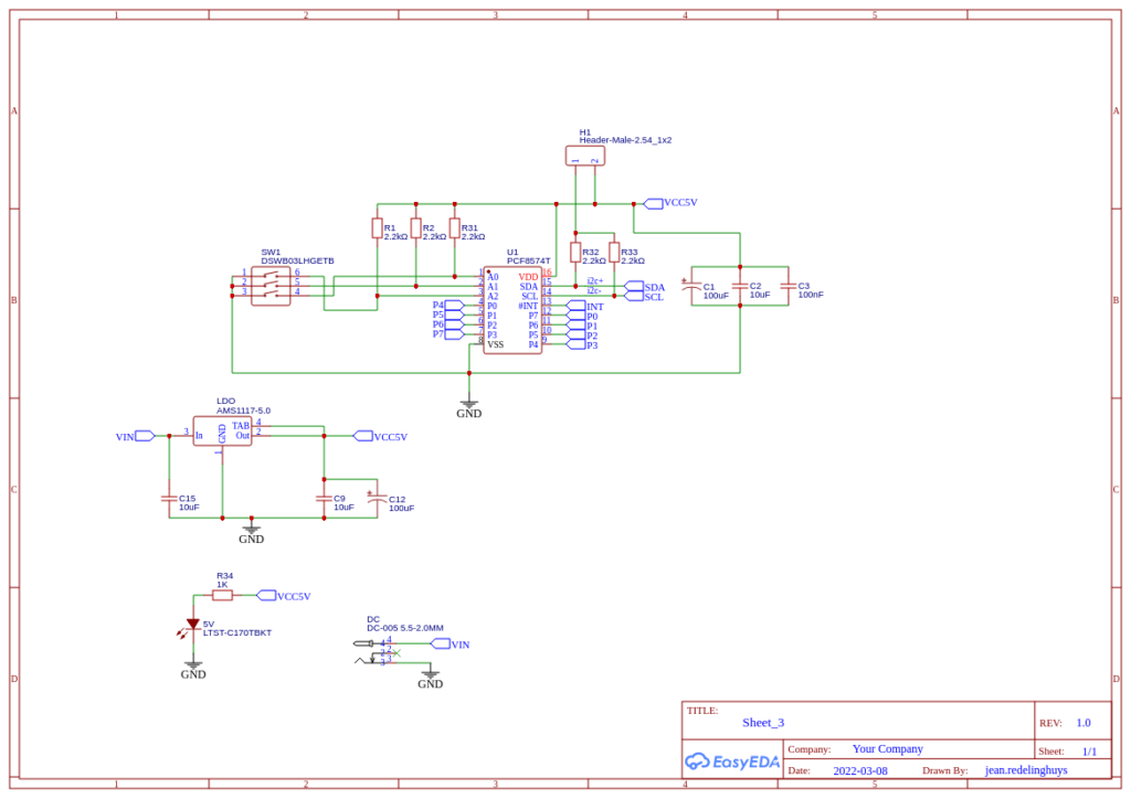
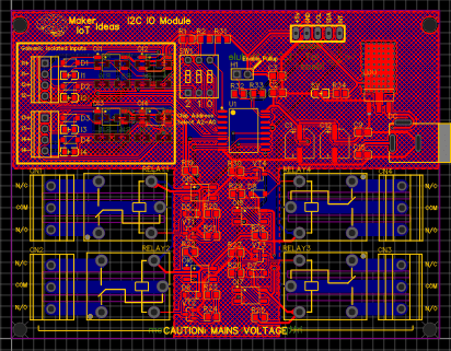
The I2C IO Card for ESP-12E I2C Base Card is another expander card for the ESP-12E I2C Base Card Project. This PCB is an address-selectable I2C module with two relays and six (6) GPIO pins, all driven from a single PCF8574 running at 3v. The relays are optically isolated, and generous mains isolation cutouts were provided to reduce the possibility of mains voltage tracking. A jumper to enable/disable the i2c pullup-resistors is also provided on the PCB.
The relays are powered from a single LDO regulator, accepting 12v DC from the 2x20pin female header on the bottom of the card. 3.3v and ground should also be applied to the card at the 2x20pin header.
It is worth mentioning that this circuit does not contain level converting circuitry and that the i2c bus thus runs at 3.3v to be compatible with ESP chips.
It is possible to use the card with other processors if the appropriate level converters are used on the i2c bus.
The Schematic
Manufacturing the PCB
Over the past eight years, PCBWay has continuously upgraded their MANUFACTURING plants and equipment to meet higher quality requirements, and now THEY also provide OEM services to build your products from ideas to mass production and access to the market.
The PCB for this project has been manufactured at PCBWay. Please consider supporting them if you would like your own copy of this PCB, or if you have any PCB of your own that you need to have manufactured.
If you would like to have PCBWAY manufacture one of your own, designs, or even this particular PCB, you need to do the following… 1) Click on this link 2) Create an account if you have not already got one of your own. If you use the link above, you will also instantly receive a $5 USD coupon, which you can use on your first or any other order later. (Disclaimer: I will earn a small referral fee from PCBWay. This referral fee will not affect the cost of your order, nor will you pay any part thereof.) 3) Once you have gone to their website, and created an account, or login with your existing account,
4) Click on PCB Instant Quote
5) If you do not have any very special requirements for your PCB, click on Quick-order PCB
6) Click on Add Gerber File, and select your Gerber file(s) from your computer. Most of your PCB details will now be automatically selected, leaving you to only select the solder mask and silk-screen colour, as well as to remove the order number or not. You can of course fine-tune everything exactly as you want as well.
7) You can also select whether you want an SMD stencil, or have the board assembled after manufacturing. Please note that the assembly service, as well as the cost of your components, ARE NOT included in the initial quoted price. ( The quote will update depending on what options you select ).
8) When you are happy with the options that you have selected, you can click on the Save to Cart Button. From here on, you can go to the top of the screen, click on Cart, make any payment(s) or use any coupons that you have in your account.
Then just sit back and wait for your new PCB to be delivered to your door via the shipping company that you have selected during checkout.
In this, part 3 of the “Giving new Life to an Old Toy Car” series, we will be adding some flashing lights to the toy car project. This will ultimately serve two purposes, with the most obvious being to give some life and excitement to the project ( as the final user will be a young boy of 7, the visual aspect is important). The second purpose is more obscured, and mostly only useable to programmers and coders, or those that will debug the project… The flashing lights will function as status indicators, at startup, as well as during the normal operation of the toy. Obviously, the diagnostic nature should be well obscured so as to not distract from the visual aspects.
A short test of the display unit, disguised as a “police-style” flasher unit
The flasher unit is made up of an extremely simple circuit, with only a PCF8574 IO expander, bypass capacitors, some LED lights, and current limiting resistors.
The bottom layer of the flasher unit, shows the Io expander, bypass capacitors, and current limiting resistors.The top layer is designed to be as clean as possible, with only LEDs and some labeling
Schematic
Schematic
The schematic is straightforward, with no surprises, consisting only of a few components, like the PCB8574, bypass capacitors, current limiting resistors, and of course the LEDs. It is also important to remember that I plan to use this entire robot car to teach a young boy to program microprocessors. I believe that visual is best, thus, all the lights 🙂
Coding
As this is still a project in quite a lot of development stages, I will not publish my exact code at this moment. You can however look forward to the future conclusion post, which will contain all my code at that stage. For now, however, we need to keep in mind that the PCF8574 is an I2C port expander, with an 8-bit IO port.
It is thus possible to do something simple like the below:
#include <Wire.h>

void setup() {
 wire.begin();
 wire.beginTransmission(0x20);
 wire.write(0b11111111); // All LEDS off
 // our circuit is sinking current into the io expander
 wire.endTransmission();
delay(1000); // delay for illustration purposes, production code will use
// non blocking code
wire.beginTransmission(0x20);
 wire.write(0b10100101); // All blue LED on
 // our circuit is sinking current into the io expander
 wire.endTransmission();
delay(1000);
}

void loop() {
}
Obviously, this is just a very quick example and is meant to just test functionality. Your own application will ultimately determine the exact code that you would need.
Manufacturing the PCB
The PCB for this project is currently on its way from China, after having been manufactured at PCBWay. Please consider supporting them if you would like your own copy of this PCB, or if you have any PCB of your own that you need to be manufactured.
If you would like to have PCBWAY manufacture one of your own, designs, or even this particular PCB, you need to do the following… 1) Click on this link 2) Create an account if you have not already got one of your own. If you use the link above, you will also instantly receive a $5USD coupon, which you can use on your first or any other order later. (Disclaimer: I will earn a small referral fee from PCBWay. This referral fee will not affect the cost of your order, nor will you pay any part thereof.) 3) Once you have gone to their website, and created an account, or login with your existing account,
4) Click on PCB Instant Quote
5) If you do not have any very special requirements for your PCB, click on Quick-order PCB
6) Click on Add Gerber File, and select your Gerber file(s) from your computer. Most of your PCB details will now be automatically selected, leaving you to only select the solder mask and silk-screen colour, as well as to remove the order number or not. You can of course fine-tune everything exactly as you want as well.
7) You can also select whether you want an SMD stencil, or have the board assembled after manufacturing. Please note that the assembly service, as well as the cost of your components, ARE NOT included in the initial quoted price. ( The quote will update depending on what options you select ).
8) When you are happy with the options that you have selected, you can click on the Save to Cart Button. From here on, you can go to the top of the screen, click on Cart, make any payment(s) or use any coupons that you have in your account.
Then just sit back and wait for your new PCB to be delivered to your door via the shipping company that you have selected during checkout.
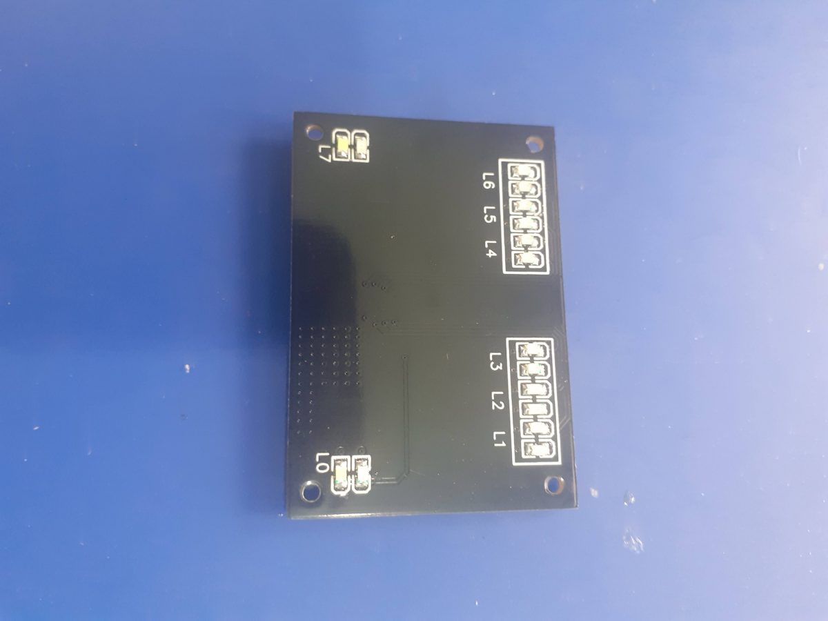
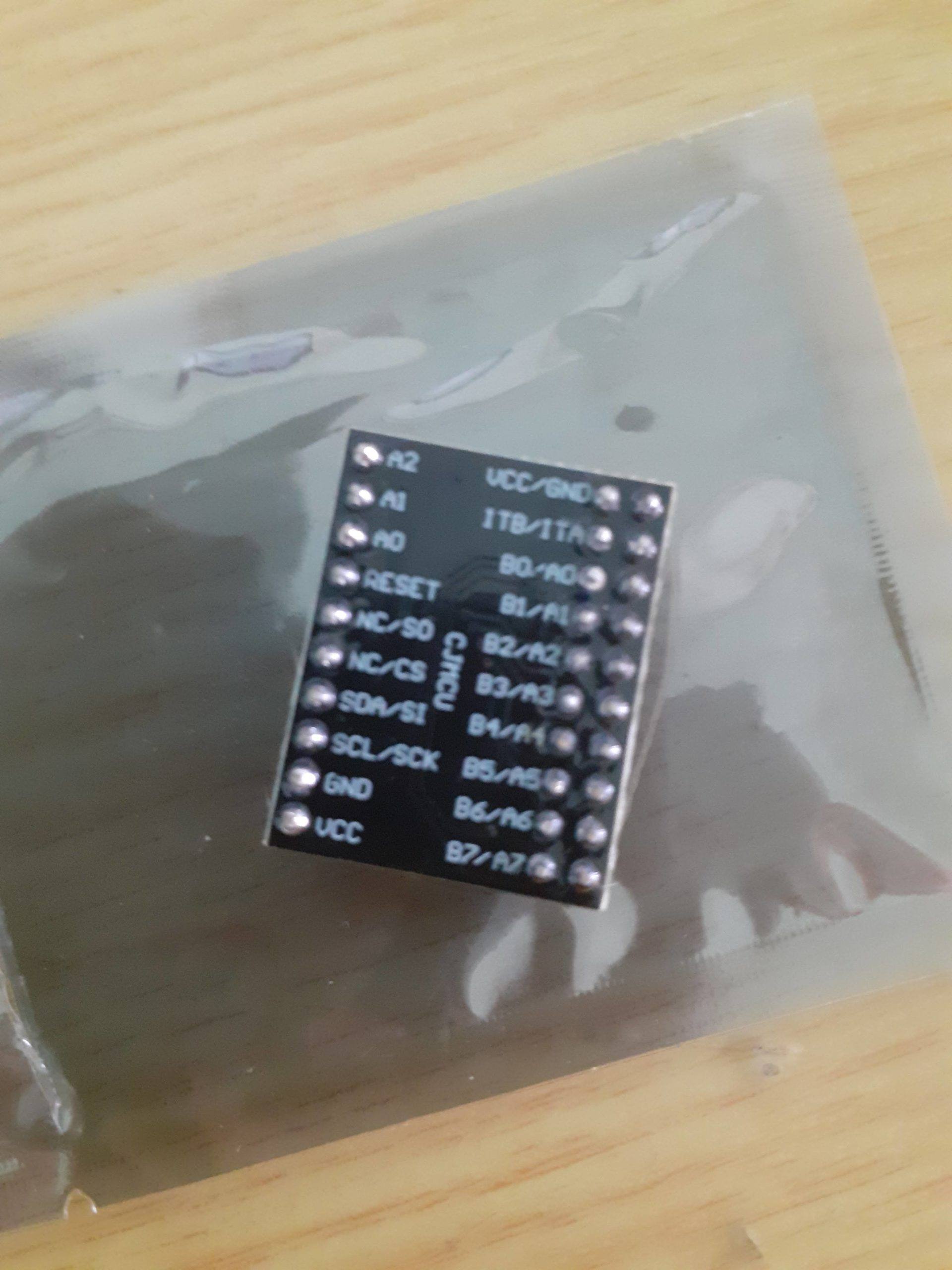
I2C port extenders or expanders are extremely useful devices, and I use quite a lot of them in my projects. My go-to device is definitely the PCF8574, mainly because it is sort of “breadboard friendly”. The MCP23017, with the existing breakouts available locally, are not. I have thus decided to design my own version of a breadboard friendly MCP23017 breakout board.
The Breakout Module PCB and its features
A breadboard friendly MCP23017 breakout board – Fronta breadboard friendly MCP23017 breakout board – Back
While this was definitely one of my easier projects, It still took a bit of time to get it just right and add some essential components and features directly onto the PCB.
The main features of this breakout: – DIP12 Layout – with all pins broken out, address pins to jumper headers… – Proper decoupling capacitors, as close as possible to the MCP23017 chip. I had to make use of the back layer of the PCB to do this, not exactly ideal, but with proper power and ground planes, and nice thick tracks, I believe they will be just fine.
– Address selector jumpers – The breakouts that are available locally, do not have these. – Breadboard friendly layout – 33.020mm x 20.320mm [board size], with 15.240mm vertical spacing between the rows of pins, ensures that you can easily fit it onto your breadboard, while still having space to add jumper wires to the pins. Horizontal pin spacing is standard 2.45mm.
The Schematic
The schematic is plain and simple. A few points to note though: – The address selection header, as well as the io pin headers are not shown on the schematic. – I2C pullup resistors are set at 1k but can be replaced with more suitable values as required in your circuit
The PCB for this project is currently on its way from China, after having been manufactured at PCBWay. Please consider supporting them if you would like your own copy of this PCB, or if you have any PCB of your own that you need to be manufactured.
If you would like to have PCBWAY manufacture one of your own, designs, or even this particular PCB, you need to do the following… 1) Click on this link 2) Create an account if you have not already got one of your own. If you use the link above, you will also instantly receive a $5USD coupon, which you can use on your first or any other order later. (Disclaimer: I will earn a small referral fee from PCBWay. This referral fee will not affect the cost of your order, nor will you pay any part thereof.) 3) Once you have gone to their website, and created an account, or login with your existing account,
4) Click on PCB Instant Quote
5) If you do not have any very special requirements for your PCB, click on Quick-order PCB
6) Click on Add Gerber File, and select your Gerber file(s) from your computer. Most of your PCB details will now be automatically selected, leaving you to only select the solder mask and silk-screen colour, as well as to remove the order number or not. You can of course fine-tune everything exactly as you want as well.
7) You can also select whether you want an SMD stencil, or have the board assembled after manufacturing. Please note that the assembly service, as well as the cost of your components, ARE NOT included in the initial quoted price. ( The quote will update depending on what options you select ).
8) When you are happy with the options that you have selected, you can click on the Save to Cart Button. From here on, you can go to the top of the screen, click on Cart, make any payment(s) or use any coupons that you have in your account.
Then just sit back and wait for your new PCB to be delivered to your door via the shipping company that you have selected during checkout.
Sometimes we need extra Inputs or Outputs on a device, or for use with a project. To implement it properly we also need a lot of additional electronic components to properly isolate these inputs and outputs, with the signals they switch, from our own project, because, let us be real, electronics and electrical devices in the real world do not all work with Arduino or ESP32/ESP8266 save voltages ( 5v and 3.3v ).
I will also tell you about a very special deal to get PCBs of your own made for only one (1) USD ( Including shipping with DHL )! No, I am not joking, and I am not crazy either… More on that later in the post…
It is thus extremely important to have a module that can effectively interface with inputs of 5.5v up to 32v DC ( optically Isolated up to 3000v ), and relay outputs, also optically isolated at 3000v. ( Note that the optical isolation voltage does not mean you can input that voltage level into the chip! It means that it can isolate the electronics on the safe side of the isolator from a voltage spike of up to that voltage!).
I also love using I2C, as it allows me to add modules onto an existing data bus while using only 2 GPIO lines on the MCU!
The module I am presenting to you today was designed to be operated from 5v DC. That includes the I2C data lines (SDA and SCL). If you need to interface to a 3.3v microprocessor, like an ESP32 or ESP8266, or even the new RP2040 or an STM32, you need to use a logic level converter.
The PCB uses the popular PCF8574 8 channel IO expander, which is extremely easy to use, and where you can connect up to 8 devices in a chain ( 16 if you use the PCF8574AT variant as well.. Meaning eight of each variant) This surely adds up to quite a lot of IO lines at a cost of only 2 GPIO on your MCU!
The Circuit diagram is below, and I will discuss each part briefly.
Schematic – Page 1
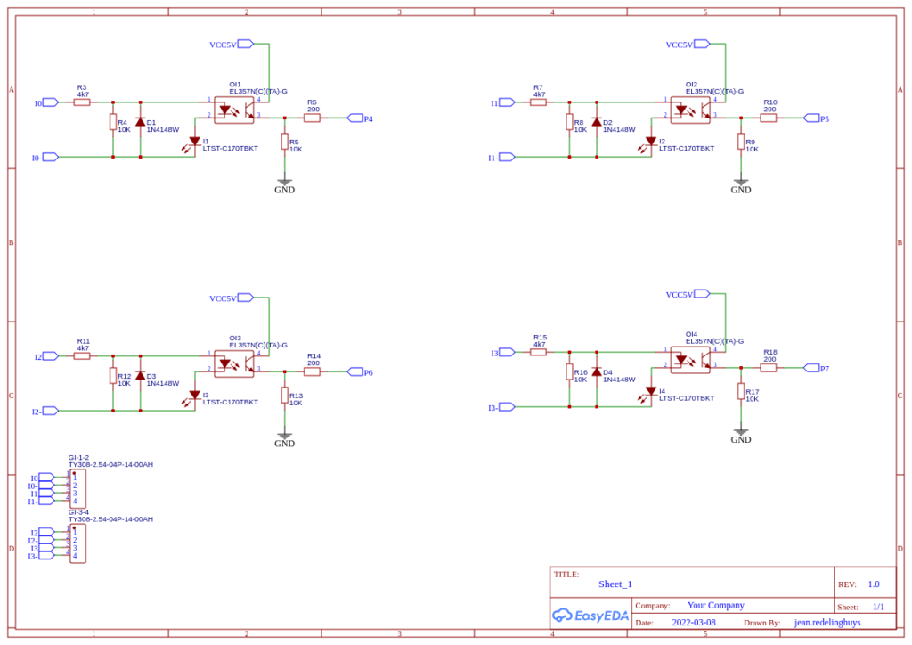
This is the Galvanic Isolated Input schematic. Each input operates at a voltage of 5.5v to 32v DC. Complete Galvanic Isolation between the Module and the remote input is in effect. Please note that you have to supply a remote ground from the device that provides the input. DO NOT connect the PCB Module ground to an isolated ground pin. This may still work but renders the galvanic Isolation for that input completely useless.
Relay Driver Schematic
This is the Relay driver schematic. Each relay output is driven through an optocoupler, as well as a transistor. Although this arrangement does not provide complete galvanic Isolation of the relay coil, it does protect your MCU from any voltage spikes caused by back-emf when the relay is de-energised. The Relay contacts themselves, being magnetically actuated by the coil, are in themselves Galvanically Isolated from the rest of the PCB.
I2C Control Schematic
Finally, we have the I2C IO Expander schematic, with a 5v LDO regulator, capable of providing up to 600mA of current to the PCB. The PCF8574 Chip’s address is selectable with DipSwitch SW1 so that you can use multiple PCBs at the same time if you should choose to do so. The only note on that is that you should not connect the 5v lines of each individual PCB together. You should also only connect the GND and SDA, SCL lines back to the MCU.
Raw PCB Layout
Earlier on in the post, I promised to tell you about a very special deal…
Well, here it is, as well as some details about the sponsor of this very exciting deal…
PCBPartner.com is owned and operated by Kinji Group, which was established in 1997. We have over 20 years of experience in PCB manufacturing, PCB design, component manufacturing and distribution, PCB assembly and PCB cam software development.
While Kinji Group has 3 PCB factories in China, we have also developed strategic partnerships with more than 15 other factories around Asia. We, therefore, have a large group of specialists in PCB manufacturing, quality control, technical support and part sourcing to support your innovative ideas and products.
Our over 500 employees are spread across 8 branches in Mainland China (Shenzhen, Dongguan, Shanghai, Wuxi, Chengdu, Xiamen), Hong Kong SAR, and Taiwan. And we’re still growing!
We’re confident once you try us out, we’ll become your PCB Partner. And if not? Well, you’ll have scored some free PCB! So why not take us for a spin, you’ve got nothing to lose.
We, MakerIoT2020.com, have decided to give it a go and send this particular PCB to PCBPartner.com for manufacturing. So far, while we are still waiting to receive the PCB, ( Weekends happen 🙂 ), We are very happy with the ease of use of the online ordering system provided.
We would also like to point out that this special order will only be available until the end of March 2022, as well as that there are a few conditions:
Promotion ends March 31st 2022 Each new customer can enjoy free PCB on their first order This promotion applies to 1-2 layers of FR4 PCB, up to 100x100mm, 10pcs, with Green Solder Mask 4 layer of FR4 PCB, up to 50x50mm, 10pcs, with Green Solder Mask 1 layer Aluminum PCB, up to 100x100mm, 10pcs This PCB promotion cannot be used with other discounts or other promotional activities
For a full list of conditions, and countries that may participate in this offer, please click on the link here
Let us have a look at the entire ordering process..
Once you click on the PCBPartner.com link, you will be taken to their website, where you should sign up, which is free and easy… We used our Google.com account details and were ready to order in seconds…
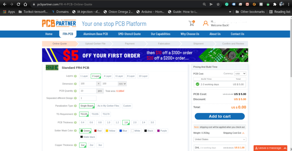
FR4 PBC Quote Form – Before uploading your Gerber Files
Enter the specific details for the manufacturing of your PCB, and upload your Gerber files.
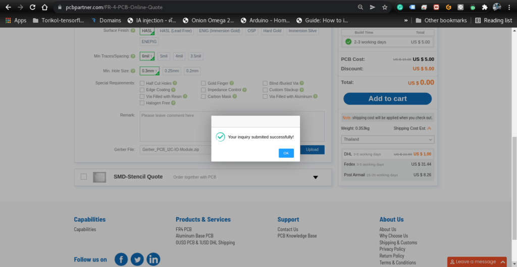
After uploading your Gerber Files.
Continue selecting options for your PCB order… Make sure to select DHL shipping, to take advantage of the special 1USD option, and click on the ADD to Cart Button…
Quote added to your shopping cart.
You will now get a message that your enquiry has been submitted successfully.
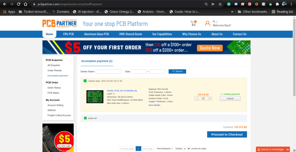
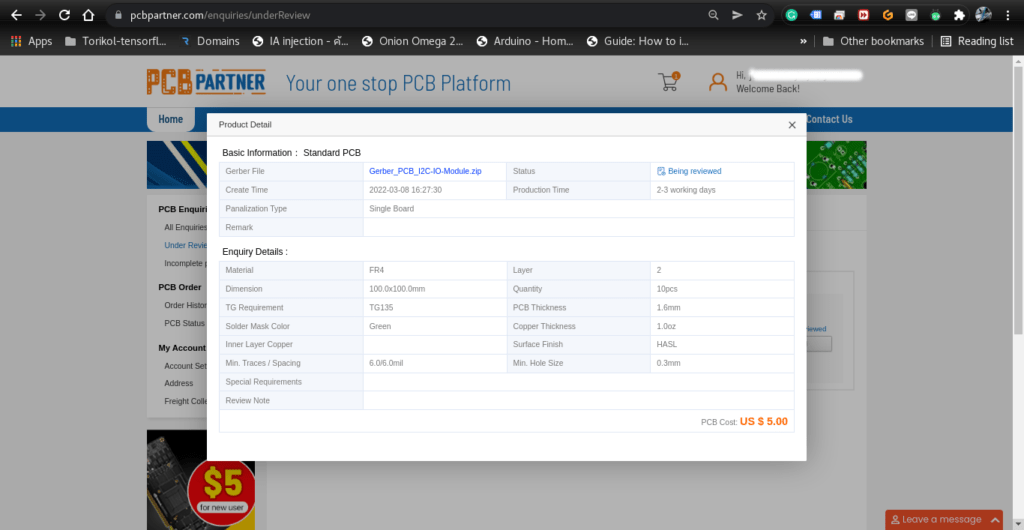
Click on the “Under review” button, to see your quote status… In my case, it took about 5 minutes for the review to pass, and be able to checkout and pay for the order…
PCB order under review
Once the review has passed, you will see a pending payment,
Payment Pending
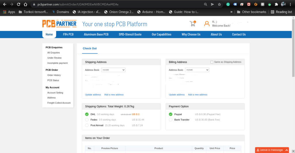
You may now click on the “Proceed to Payment” option
Add your shipping address, and choose your payment option.
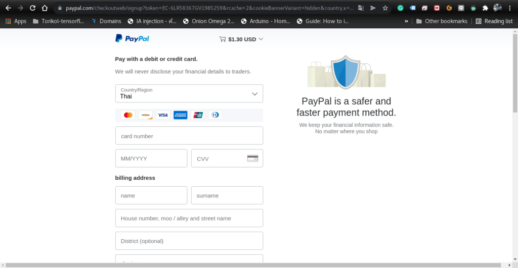
At this moment in time, only two payment options are supported, Paypal ( as well as Debit and Credit cards) and Direct Bank Transfer. I believe more options will be made available in future.. Checkout with Paypal
In my case, I chose Paypal and paid by Debit card.
Enter your card detailsAfter Payment.
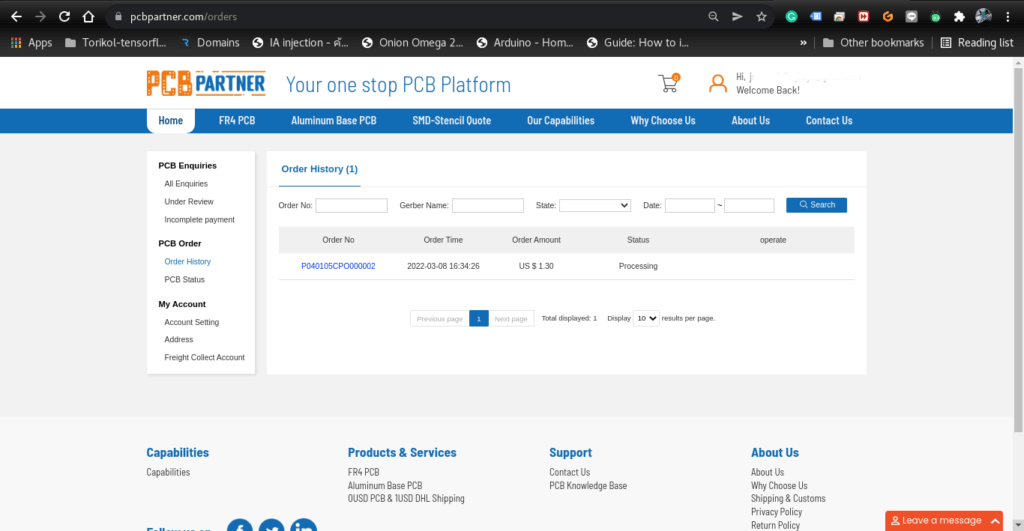
After payment was made successfully, you can also check on the status of your order…
Review your order status
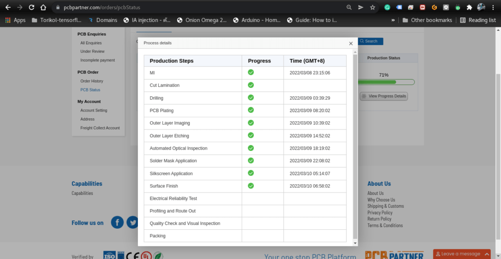
You can also review your order at any stage before or after payment, as well as get progress reports of the manufacturing process.
PCB Order Status.
In conclusion, I would like to say that it was quite easy to order and make payment. The Website is easy to use, and everything is clear and easy to understand. The PCB was well manufactured and seems to be quite good quality
In a previous post, I have shown you how to use the MCP23017 16 Port I2C I/O Port extender with the standard Wire library, as supplied with the Arduino IDE. In this post, I will have a quick look at using Adafruit’s library for this IC. I believe that this library brings a lot of ease-of-use to the part, making it possible to obscure some of the complexity of I2C.
I do however prefer to use the native Wire library myself, as it is slightly faster.
When using single pin operations such as pinMode(pinId, dir) or digitalRead(pinId) or digitalWrite(pinId, val) then the pins are addressed using the ID’s below. For example, for set the mode of GPB0 then use pinMode(8, …).
Physical Pin #
Pin Name
Pin ID
21
GPA0
0
22
GPA1
1
23
GPA2
2
24
GPA3
3
25
GPA4
4
26
GPA5
5
27
GPA6
6
28
GPA7
7
1
GPB0
8
2
GPB1
9
3
GPB2
10
4
GPB3
11
5
GPB4
12
6
GPB5
13
7
GPB6
14
8
GPB7
15
Some examples, directly from the library, all code belongs to Adafruit, and was not written by me.
1. A Button Example
#include <Wire.h>
#include "Adafruit_MCP23017.h"

// Basic pin reading and pullup test for the MCP23017 I/O expander
// public domain!

// Connect pin #12 of the expander to Analog 5 (i2c clock)
// Connect pin #13 of the expander to Analog 4 (i2c data)
// Connect pins #15, 16 and 17 of the expander to ground (address selection)
// Connect pin #9 of the expander to 5V (power)
// Connect pin #10 of the expander to ground (common ground)
// Connect pin #18 through a ~10kohm resistor to 5V (reset pin, active low)

// Input #0 is on pin 21 so connect a button or switch from there to ground

Adafruit_MCP23017 mcp;

void setup() {
  mcp.begin();      // use default address 0

  mcp.pinMode(0, INPUT);
  mcp.pullUp(0, HIGH);  // turn on a 100K pullup internally

  pinMode(13, OUTPUT);  // use the p13 LED as debugging
}


void loop() {
  // The LED will 'echo' the button
  digitalWrite(13, mcp.digitalRead(0));
}
2. An Interrupt Example
// Install the LowPower library for optional sleeping support.
// See loop() function comments for details on usage.
//#include <LowPower.h>

#include <Wire.h>
#include <Adafruit_MCP23017.h>

Adafruit_MCP23017 mcp;

byte ledPin=13;

// Interrupts from the MCP will be handled by this PIN
byte arduinoIntPin=3;

// ... and this interrupt vector
byte arduinoInterrupt=1;

volatile boolean awakenByInterrupt = false;

// Two pins at the MCP (Ports A/B where some buttons have been setup.)
// Buttons connect the pin to grond, and pins are pulled up.
byte mcpPinA=7;
byte mcpPinB=15;

void setup(){

  Serial.begin(9600);
  Serial.println("MCP23007 Interrupt Test");

  pinMode(arduinoIntPin,INPUT);

  mcp.begin();      // use default address 0

  // We mirror INTA and INTB, so that only one line is required between MCP and Arduino for int reporting
  // The INTA/B will not be Floating
  // INTs will be signaled with a LOW
  mcp.setupInterrupts(true,false,LOW);

  // configuration for a button on port A
  // interrupt will triger when the pin is taken to ground by a pushbutton
  mcp.pinMode(mcpPinA, INPUT);
  mcp.pullUp(mcpPinA, HIGH);  // turn on a 100K pullup internally
  mcp.setupInterruptPin(mcpPinA,FALLING);

  // similar, but on port B.
  mcp.pinMode(mcpPinB, INPUT);
  mcp.pullUp(mcpPinB, HIGH);  // turn on a 100K pullup internall
  mcp.setupInterruptPin(mcpPinB,FALLING);

  // We will setup a pin for flashing from the int routine
  pinMode(ledPin, OUTPUT);  // use the p13 LED as debugging

}

// The int handler will just signal that the int has happen
// we will do the work from the main loop.
void intCallBack(){
  awakenByInterrupt=true;
}

void handleInterrupt(){

  // Get more information from the MCP from the INT
  uint8_t pin=mcp.getLastInterruptPin();
  uint8_t val=mcp.getLastInterruptPinValue();

  // We will flash the led 1 or 2 times depending on the PIN that triggered the Interrupt
  // 3 and 4 flases are supposed to be impossible conditions... just for debugging.
  uint8_t flashes=4;
  if(pin==mcpPinA) flashes=1;
  if(pin==mcpPinB) flashes=2;
  if(val!=LOW) flashes=3;

  // simulate some output associated to this
  for(int i=0;i<flashes;i++){
    delay(100);
    digitalWrite(ledPin,HIGH);
    delay(100);
    digitalWrite(ledPin,LOW);
  }

  // we have to wait for the interrupt condition to finish
  // otherwise we might go to sleep with an ongoing condition and never wake up again.
  // as, an action is required to clear the INT flag, and allow it to trigger again.
  // see datasheet for datails.
  while( ! (mcp.digitalRead(mcpPinB) && mcp.digitalRead(mcpPinA) ));
  // and clean queued INT signal
  cleanInterrupts();
}

// handy for interrupts triggered by buttons
// normally signal a few due to bouncing issues
void cleanInterrupts(){
  EIFR=0x01;
  awakenByInterrupt=false;
}

/**
 * main routine: sleep the arduino, and wake up on Interrups.
 * the LowPower library, or similar is required for sleeping, but sleep is simulated here.
 * It is actually posible to get the MCP to draw only 1uA while in standby as the datasheet claims,
 * however there is no stadndby mode. Its all down to seting up each pin in a way that current does not flow.
 * and you can wait for interrupts while waiting.
 */
void loop(){

  // enable interrupts before going to sleep/wait
  // And we setup a callback for the arduino INT handler.
  attachInterrupt(arduinoInterrupt,intCallBack,FALLING);

  // Simulate a deep sleep
  while(!awakenByInterrupt);
  // Or sleep the arduino, this lib is great, if you have it.
  //LowPower.powerDown(SLEEP_1S, ADC_OFF, BOD_OFF);

  // disable interrupts while handling them.
  detachInterrupt(arduinoInterrupt);

  if(awakenByInterrupt) handleInterrupt();
}


I hope that this shows you another way of using this versatile IC,
In a future post, I will show you how to do interrupts, using the native Wire library, as well as point out a few things about why interrrupts sometimes does not seem to be working, as well as a workaround for that.
Today I will show you another useful IO Expander chip, The MCP23017. This chip, although similar to the PCF8475, which I have already covered in a previous article, has many additional features that may make it a very attractive solution when you need some more extra GPIO pins for a big project…
Features
Let us look at some of the features of this chip
16-Bit Remote Bidirectional I/O Port:
I/O pins default to input • High-Speed I2C Interface (MCP23017):
100 kHz
400 kHz
1.7 MHz • High-Speed SPI Interface (MCP23S17):
10 MHz (maximum) • Three Hardware Address Pins to Allow Up to Eight Devices On the Bus • Configurable Interrupt Output Pins:
Configurable as active-high, active-low or open-drain • INTA and INTB Can Be Configured to Operate Independently or Together • Configurable Interrupt Source:
Interrupt-on-change from configured register defaults or pin changes • Polarity Inversion Register to Configure the Polarity of the Input Port Data • External Reset Input • Low Standby Current: 1 µA (max.) • Operating Voltage:
1.8V to 5.5V @ -40°C to +85°C
2.7V to 5.5V @ -40°C to +85°C
4.5V to 5.5V @ -40°C to +125°C
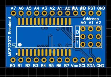
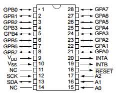
MCP23017 Pinout Diagram
The sixteen I/O ports are separated into two ‘ports’ – A (on the right) and B (on the left. Pin 9 connects to 5V, 10 to GND, 11 isn’t used, 12 is the I2C bus clock line (Arduino Uno/Duemilanove analogue pin 5, Mega pin 21), and 13 is the I2C bus data line (Arduino Uno/Duemailnove analogue pin 4, Mega pin 20).
External pull-up resistors should be used on the I2C bus – in our examples we use 4.7k ohm values. Pin 14 is unused, and we won’t be looking at interrupts, so ignore pins 19 and 20. Pin 18 is the reset pin, which is normally high – therefore you ground it to reset the IC. So connect it to 5V!
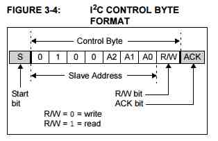
Finally we have the three hardware address pins 15~17. These are used to determine the I2C bus address for the chip. If you connect them all to GND, the address is 0x20. If you have other devices with that address or need to use multiple MCP23017s, see figure 1-2 in the datasheet.
You can alter the address by connecting a combination of pins 15~17 to 5V (1) or GND (0). For example, if you connect 15~17 all to 5V, the control byte becomes 0100111 in binary, or 0x27 in hexadecimal.
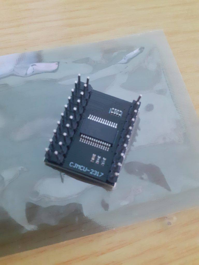
It is also available on a convenient breakout PCB, for about $USD0.80 from AliExpress
MCP23017 on Breakout PCB – Back
MCP23017 on Breakout PCB – Front
Please Note: THIS BREAKOUT PCB IS NOT SUITED FOR USE ON A BREADBOARD. YOU WILL SHORT OUT VCC AND GROUND AS WELL AS ALL THE IO PINS IF YOU TRY TO USE IT ON A BREADBOARD.
As you can see, the pins are however very clearly labelled, and thus easy to use. I have also purposely soldered my header pins “the wrong way round” to prevent using it on a breadboard, as this will short out Vcc to Ground!
Having interrupt outputs is one of the most important features of the MCP23017, since the microcontroller does not have to continuously poll the device to detect an input change. Instead an interrupt service routine can be used to react quickly to an input change such a key press…
To make life even easier each GPIO input pin can be configured with an internal pullup (~100k) and that means you won’t have to wire up external pull up resistors for keyboard input. You can also mix and match inputs and outputs the same as any standard microcontroller 8 bit port.
Addressing
The 23017 has three input pins to allow you to set a different address for each attached MCP23017.
The above corresponds to a hardware address for the three lines A0, A1, A2 corresponding to the input pin values at the IC. You must set the value of these hardware inputs as 0V or (high) volts and not leave them floating otherwise they will get random values from electrical noise and the chip will do nothing!
The four left most bits are fixed a 0100 (specified by a consortium who doles out address ranges to manufacturers).
So the MCP23017 I2C address range is 32 decimal to 37 decimal or 0x20 to 0x27 for the MCP23017.
Please note: The addresses are the same as those for the PCF8475. You must thus be careful if you use these two devices on the same i2c bus!
MCP23017 Non interrupt registers
IODIR I/O direction register
For controlling I/O direction of each pin, register IODIR (A/B) lets you set the pin to an output when a zero is written and to an input when a ‘1’ is written to the register bit. This is the same scheme for most microcontrollers – the key is to remember that zero (‘0’) equates to the ‘O’ in Output.
GPPU Pullup register
Setting a bit high sets the pullup active for the corresponding I/O pin.
OLAT Output Latch register
This is exactly the same as the I/O port in 18F series PIC chips where you can read back the “desired” output of a port pin whether or not the actual state of that pin is reached. i.e. consider a strong current LED attached to the pin – it is easily possible to pull down the output voltage at the pin to below the logic threshold i.e. you would read back a zero if reading from the pin itself when in fact it should be a one. Reading the OLAT register bit returns a ‘one’ as you would expect from a software engineering point of view.
IPOL pin inversion register
The IPOL(A/B) register allows you to selectively invert any input pin. This reduces the glue logic needed to interface other devices to the MCP23017 since you won’t need to add inverter logic chips to get the correct signal polarity into the MCP23017.
It is also very handy for getting the signals the right way up e.g. it is common to use a pull up resistor for an input so when a user presses an input key the voltage input is zero, so in software you have to remember to test for zero.
Using the MCP23017 you could invert that input and test for a 1 (in my mind a key press is more equivalent to an on state i.e. a ‘1’) however I use pullups all the time (and uCs in general use internal pullups when enabled) so have to put up with a zero as ‘pressed’. Using this device would allow you to correct this easily.Note: The reason that active low signals are used everywhere is a historical one: TTL (Transistor Transistor Logic) devices draw more power in the active low state due to the internal circuitry, and it was important to reduce unnecessary power consumption – therefore signals that are inactive most of the time e.g. a chip select signal – were defined to be high. With CMOS devices either state causes the same power usage so it now does not matter – however active low is used because everyone uses it now and used it in the past.
SEQOP polling mode : register bit : (Within IOCON register)
If you have a design that has critical interrupt code e.g. for performing a timing critical measurement you may not want non critical inputs to generate an interrupt i.e. you reserve the interrupt for the most important input data.
In this case, it may make more sense to allow polling of some of the device inputs. To facilitate this “Byte mode” is provided. In this mode, you can read the same set of GPIOs using clocks but not needling to provide other control information. i.e. it stays on the same set of GPIO bits, and you can continuously read it without the register-address updating itself. In non-byte mode, you either have to set the address you read from (A or B bank) as control input data.
Now to examine how to use the IC in our sketches.
As you should know by now most I2C devices have several registers that can be addressed. Each address holds one byte of data that determines various options. So before using we need to set whether each port is an input or an output. First, we’ll examine setting them as outputs. So to set port A to outputs, we use:
Wire.beginTransmission(0x20);
Wire.write(0x00); // IODIRA register
Wire.write(0x00); // set all of port A to outputs
Wire.endTransmission();
Then to set port B to outputs, we use:
Wire.beginTransmission(0x20);
Wire.write(0x01); // IODIRB register
Wire.write(0x00); // set all of port B to outputs
Wire.endTransmission();
So now we are in void loop() or a function of your own creation and want to control some output pins. To control port A, we use:
Wire.beginTransmission(0x20);
Wire.write(0x12); // address port A
Wire.write(??);  // value to send
Wire.endTransmission();
To control port B, we use:
Wire.beginTransmission(0x20);
Wire.write(0x13); // address port B
Wire.write(??);  // value to send
Wire.endTransmission();
… replacing ?? with the binary or equivalent hexadecimal or decimal value to send to the register.
To calculate the required number, consider each I/O pin from 7 to 0 matches one bit of a binary number – 1 for on, 0 for off. So you can insert a binary number representing the status of each output pin. Or if binary does your head in, convert it to hexadecimal. Or a decimal number.
So for example, you want pins 7 and 1 on. In binary that would be 10000010, in hexadecimal that is 0x82, or 130 decimal. (Using decimals is convenient if you want to display values from an incrementing value or function result).
For example, we want port A to be 11001100 and port B to be 10001000 – so we send the following (note we converted the binary values to decimal):
Wire.beginTransmission(0x20);
Wire.write(0x12); // address port A
Wire.write(204); // value to send
Wire.endTransmission();
Wire.beginTransmission(0x20);
Wire.write(0x13); // address port B
Wire.write(136);     // value to send
Wire.endTransmission();
A complete Example
// pins 15~17 to GND, I2C bus address is 0x20
#include "Wire.h"
void setup()
{
 Wire.begin(); // wake up I2C bus
// set I/O pins to outputs
 Wire.beginTransmission(0x20);
 Wire.write(0x00); // IODIRA register
 Wire.write(0x00); // set all of port A to outputs
 Wire.endTransmission();
Wire.beginTransmission(0x20);
 Wire.write(0x01); // IODIRB register
 Wire.write(0x00); // set all of port B to outputs
 Wire.endTransmission();
}
void binaryCount()
{
 for (byte a=0; a<256; a++)
 {
 Wire.beginTransmission(0x20);
 Wire.write(0x12); // GPIOA
 Wire.write(a); // port A
 Wire.endTransmission();
Wire.beginTransmission(0x20);
 Wire.write(0x13); // GPIOB
 Wire.write(a); // port B
 Wire.endTransmission();
 }
}
void loop()
{
 binaryCount();
 delay(500);
}
Using the pins as inputs
Although that may have seemed like a simple demonstration, it was created show how the outputs can be used. So now you know how to control the I/O pins set as outputs. Note that you can’t source more than 25 mA of current from each pin, so if switching higher current loads use a transistor and an external power supply and so on.
Now let’s turn the tables and work on using the I/O pins as digital inputs. The MCP23017 I/O pins default to input mode, so we just need to initiate the I2C bus. Then in the void loop() or other function all we do is set the address of the register to read and receive one byte of data.
// pins 15~17 to GND, I2C bus address is 0x20
#include "Wire.h"
byte inputs=0;
void setup()
{
 Serial.begin(9600);
 Wire.begin(); // wake up I2C bus
}
void loop()
{
 Wire.beginTransmission(0x20);
 Wire.write(0x13); // set MCP23017 memory pointer to GPIOB address
 Wire.endTransmission();
 Wire.requestFrom(0x20, 1); // request one byte of data from MCP20317
 inputs=Wire.read(); // store the incoming byte into "inputs"
 if (inputs>0) // if a button was pressed
 {
 Serial.println(inputs, BIN); // display the contents of the GPIOB register in binary
 delay(200); // for debounce
 }
}
Other Libraries
You can also download and install the MCP23017 Library from Adafruit for the Arduino IDE. This library will make using this chip even easier… I will discuss this library in another post
Using a matrix keypad is a very easy way to add multiple control buttons to a project, be it to enter a password, or to control different devices. These keypads do unfortunately have some serious flaws (in my view anyway)
1) They are usually of extremely low quality ( especially some of the membrane types from China). This means they dont last very long. 2) A typical 4×4 Matrix keypad will require 8 of your precious IO pins for itself.
These two flaws can however easily be solved, if we use a bit of technology, and are willing to to a bit of simple circuit construction by ourselves.
What does this mean ? Most of us makers will inevitably have a piece of proto-board or strip-board lying around, as well as a few momentary push-button switches. These can easily be used to make out own, much more reliable keypad. Let us look at the circuit
Circuit diagram for a 4×4 Matrix Keypad
As we can see, to build a 4×4 matrix keypad, we will need 16 momentary switches. These are connected together as shown above. You can then interface it with your favourite micro-controller to read the key(s) pressed…
This definitely solves the first of my problems, but we still need 8 pins to control this keypad… or do we? No, we don’t, we need only 2 pins. That is to say if we use one of those PCF8574 I2C IO port expander modules. They are much more reliable, as well as quite cheap as well. all depending on where you buy them from, and how long you are willing to wait for shipping 🙂
Let us see how to connect the keypad to the I2C Module
a 4×4 Membrane Matrix Keypad with PCF8574 I2C port expander moduleConnecting the two together, note that we do not connect the INT pinConnect Power (VCC, GND and I2C lines Connect to Arduino or your preferred microcontroller. We have used Arduino Uno, Note that you can also connect the I2C to A4 (SDA) and A5(SCL) if you prefer.
Now, we need to install some libraries
The first one is the actual Keypad library, you can download it from the link below
#include <Key.h>
#include <Keypad.h>
#include <Keypad_I2C.h>

#define I2CADDR 0x26 // Set the Address of the PCF8574

const byte ROWS = 4; // Set the number of Rows
const byte COLS = 4; // Set the number of Columns

// Set the Key at Use (4x4)
char keys [ROWS] [COLS] = {
  {'1', '2', '3', 'A'},
  {'4', '5', '6', 'B'},
  {'7', '8', '9', 'C'},
  {'*', '0', '#', 'D'}
};

// define active Pin (4x4)
byte rowPins [ROWS] = {0, 1, 2, 3}; // Connect to Keyboard Row Pin
byte colPins [COLS] = {4, 5, 6, 7}; // Connect to Pin column of keypad.

// makeKeymap (keys): Define Keymap
// rowPins:Set Pin to Keyboard Row
// colPins: Set Pin Column of Keypad
// ROWS: Set Number of Rows.
// COLS: Set the number of Columns
// I2CADDR: Set the Address for i2C
// PCF8574: Set the number IC
Keypad_I2C keypad (makeKeymap (keys), rowPins, colPins, ROWS, COLS, I2CADDR, PCF8574);

void setup () {
  Wire .begin (); // Call the connection Wire
  keypad.begin (makeKeymap (keys)); // Call the connection
  Serial.begin (9600);

}
void loop () {

  char key = keypad.getKey (); // Create a variable named key of type char to hold the characters pressed

  if (key) {// if the key variable contains
    Serial.println (key); // output characters from Serial Monitor
  }
}
Upload this to your Arduino device and enjoy. This sketch can also be adapted for 1×4, and 4×3 keypads, and with a little modification, will also work perfectly on ESP32 or ESP8266 as well…