
As I have hinted in my recent two posts about UPDI programmers, I am currently looking for a solution to replace the ATMEGA328P chip used in standard Arduino devices, like the UNO and NANO.
The global chip shortage seems to be still hitting hard, with these devices (Arduino UNO, NANO), and even bare chips being quite hard to get hold of, and when you do, they are quite more expensive than they used to be.
This sent me on a new journey, to find a new chip, that is easy to use, inexpensive, and easy to get hold of. I have found 3 of these chips, starting today with the ATMEGATiny202,

The ATtiny202 is a microcontroller using the 8-bit AVR® processor with a hardware multiplier, running up to 20 MHz and 2 KB Flash, 128B SRAM, and 64 bytes of EEPROM in an 8-pin package. The series uses the latest technologies from Microchip with a flexible and low-power architecture, including Event System and SleepWalking, accurate analog features and advanced peripherals.
With only 8 pins, of which we can practically use only 5 ( 6 if you have an HV UPDI programmer ). This makes it a desirable solution for small projects, with its current price of about 0.59 USD per chip ( SOIC8 PACKAGE, Element14 ) , not breaking the bank either. Not needing an external oscillator, and requiring only a single 100nf bypass capacitor, (not counting the UPDI resistor) it can indeed be a very very cheap way to get a project done… Providing of course that you don’t need a lot of Program memory or RAM, and are not trying to do too many super fancy or complicated things.

The wide operating voltage of 1.8v right up to 5.5v also makes it quite flexible.
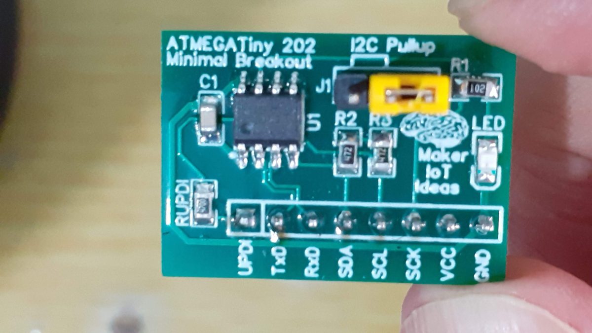
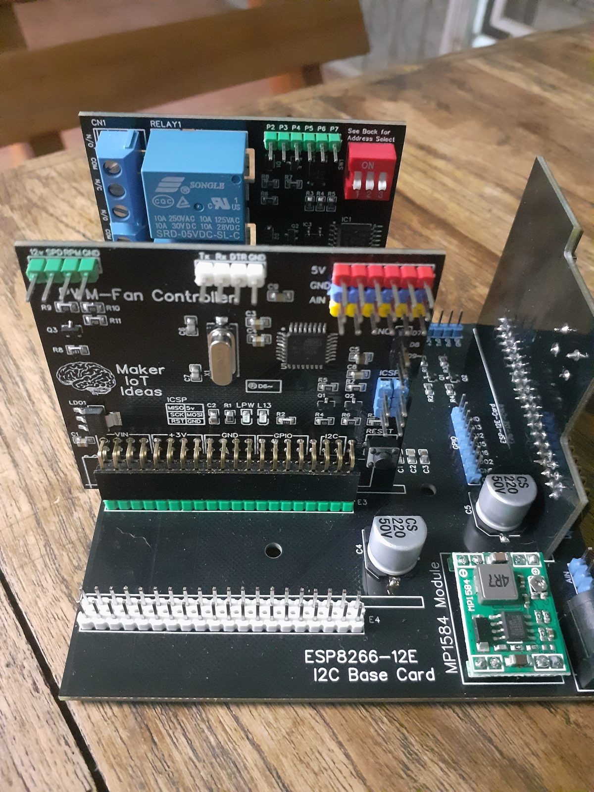
My initial prototype
Getting started with a new chip is also a bit of an issue, as there are many new things to learn, recommended supporting components, and also firmware and cores that need to be installed. I have decided to build a quick breadboard-capable PCB, with all 8 pins broken out in a single row, feel free to change the straight header pins to a 90-degree version at your convenience, it takes up even less space that way.
The PCB contains only the bare minimum required components for the chip to function, but I also added onboard I2C pullup resistors, with a jumper to select them. ( Most I2C modules usually have these already, but as I build most of my own breakouts myself, I decided to include these).
A single LED brightens things up a bit, connected to pin PA3, making it possible to run a blink sketch…
The rest of the components include a 100nf bypass capacitor and the very important 470ohm UPDI resistor.


Programming the board
I use the Arduino IDE quite a lot, and also assume that most makers and hobbyists out there will do the same. Luckily we have access to a special Arduino core, the megaTinyCore, that provides us with all we need to program this tiny little chip, provided of course that you have a UPDI programmer.
See the link above for installation instructions, as well as detailed documentation. Replicating all of that here will be an unnecessary task, as the author of the core, SpenceKonde, has already done an excellent job.
One very important thing to note on this board is that there is NO RESET PIN.
You have to manually cycle power to it, but, I have found that initiating a UPDI upload to a running chip works every time, and makes it unnecessary…
The reason for the lack of a reset pin lies in the fact that the reset is shared with the UPDI pin, and enabling it, will rob you of the UPDI functionality UNLESS you have an HV UPDI programmer, which at this time seems to be hard to find/expensive item ( Hope to build my own soon). Once again, see the above link to the core documentation for the full information on the reset pin issue…
I can not stress enough how important it is to sit down and READ the core documentation, with attention, before doing anything with this chip and core. you will learn a lot, about the chip, new features, possible problems, and how to avoid them, and also some customised GPIO functions etc…
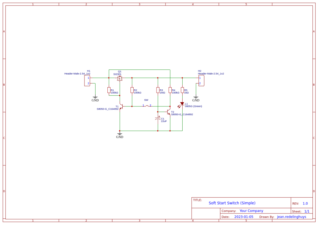
Schematic

Manufacturing

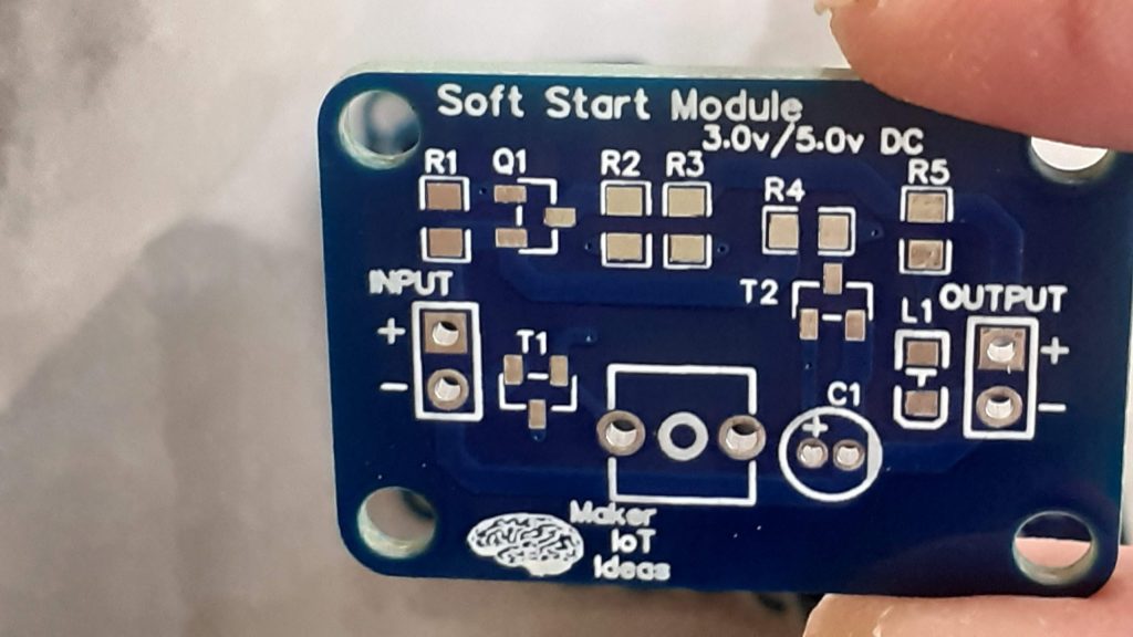
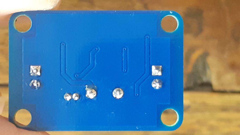
The PCB is a double-layer PCB, with the signal traces on the top layer, power traces, and the ground-plane, on the bottom layer. the Dimensions are 26.035mm x 18.669m. All SMD components are 0805. This board does not need a stencil for assembly and can be hand or hot-air soldered in a few minutes with no problems.
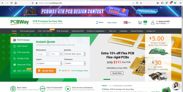
As many of my existing readers will know by now, I choose PCBWay for my PCB manufacturing. Why? What makes them different from the rest?
PCBWay‘s business goal is to be the most professional PCB manufacturer for prototyping and low-volume production work in the world. With more than a decade in the business, they are committed to meeting the needs of their customers from different industries in terms of quality, delivery, cost-effectiveness and any other demanding requests. As one of the most experienced PCB manufacturers and SMT Assemblers in China, they pride themselves to be our (the Makers) best business partners, as well as good friends in every aspect of our PCB manufacturing needs. They strive to make our R&D work easy and hassle-free.
How do they do that?
PCBWay is NOT a broker. That means that they do all manufacturing and assembly themselves, cutting out all the middlemen, and saving us money.
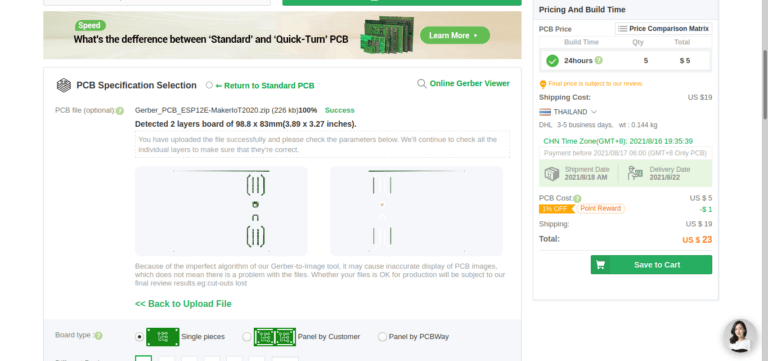
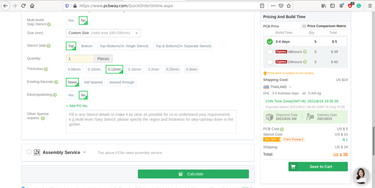
PCBWay’s online quoting system gives a very detailed and accurate picture of all costs upfront, including components and assembly costs. This saves a lot of time and hassle.
PCBWay gives you one-on-one customer support, that answers you in 5 minutes ( from the Website chat ) , or by email within a few hours ( from your personal account manager). Issues are really resolved very quickly, not that there are many anyway, but, as we are all human, it is nice to know that when a gremlin rears its head, you have someone to talk to that will do his/her best to resolve your issue as soon as possible.
Find out more here

Picture Gallery


