Most of us are familiar with voice assistants these days; Google Assistant, Siri and Alexa are obviously the most well-known of these. They all share a common problem though: They are online, and can thus secretly record everything you say around them, for later use by their respective owners [ The Companies that created them ]. Having a true offline voice assistant can thus seem like the holy grail for privacy and security-minded people.
Introducing VC-01/VC-02
I was recently contacted by AI-Thinker and asked if I was interested to play with a new product of theirs, an offline voice module. I immediately jumped at the opportunity, as this was something that I wanted to get my hands on for a long time, providing it works of course…
AI-Thinker’s offline voice module is available in two models, the VC-01 and the VC-02.
My Sales Representative (Kat ) sent me both models, in a kit format, complete with speaker and microphone. The kit PCB also provides a USB port with a ch340 chip, as well as two push buttons (reset and wake-up) as well as 3 built-in LEDs ( White, Orange and Blue ).
These light up with the factory firmware, depending on what commands are issued to the device…
Let us take a look at how the factory firmware works; Thank you to Kat from Ai-Thinker for uploading the video, and sending the link to me 🙂
As we can see in the video above, the module seems to work very well… The question now arises if it can be customised to do what we want it to…
Custom Firmware – Do-able, but with a few caveats
Information in English on this module is very sparse. This is due to it being very new, and with AI-Thinker focusing most of their efforts for this module on the Chinese market for the time being. Which makes sense in one way, but also doesn’t in another.
After spending quite a bit of time trying to get information, my Sales Rep eventually gave me access to an online configuration utility, now be warned: This is not for the faint of heart. The entire interface is in Chinese ( They are working on an English version, with time-to-completion between one (1) to four(4) weeks from starting the project. I can however not give any accurate dates at this stage, but was told that this development is underway).
Being no stranger to different languages, I thought to use google translate to translate the website. No, that didn’t work. Google refuses or the Chinese Website doesn’t allow it to?No answer as of yet. Any readers who do know any reasons for this, please comment below.
I was sort of successful in manually copy pasting line by line into google translate and got some translation back, but it was not very useful.
My next point to try was asking AI-Thinker to generate some firmware with the web tool. They gladly did that, and that works great. It is however not feasible in the long term to go that route every time.
This was possible because the AI-Thinker engineers, using the firmware development software, currently only available in Chinese, can set custom wake words and train voice commands with a 95% accuracy rate, before generating firmware and flashing it onto the respective module.
Write your own, someone will obviously say, and that was my next attempt. There is an API, and source code on GitHub, as well as Gitee ( The Chinese version of GitHub) The two sources are however not synced, and I was still not successful in getting anything useful from Gitee, once again due to a language issue, as well as the fact that some of the sources depend on 32bit dependencies for Ubuntu, whereas I am running a 64bit version… I did try it though, and can not report any success on that venture at all.
Once again, I will advice us all to wait for AI-Thinker to release an English version of the SDK and API for us all to use, which I am sure they will do at some stage in the near future.
See the video below of my custom firmware, once again demonstrated by Kat from AI-Thinker
Custom Firmware – Test 01
As we can see, it once again performs well, with a few issues, but quite acceptable…
Hardware access to the real world
As we have just seen in the video, there is also hardware access via pins, to the real world. There are however a few issues there as well…
Hardware pins are limited. I2C and SPI, although advertised, are apparently not yet supported in any of the current firmware – Someone with information, please comment…
As a proof of concept, I have decided to design a quick prototype with relays to use as a more detailed test. I will update information on that soon…
My Conclusion
I definitely see potential here. This is a product which can be quite useful in the future, providing that the following is done:
Proper detailed documentation is provided in English as well as Chinese API and SDK access is made available in English as well as Chinese Firmware be updated to make all features available
Having said all of that, I do understand that development, and especially R&D do take a lot of time. Translating documents accurately does too.
I want to congratulate AI-Thinker on producing a very well-made unit, that will definitely bring the dream of a totally offline voice assistant a little bit closer to being a reality.
Voice recognition with my bastard South-African/British English Accent, heavily influenced by Afrikaans, went extremely well, even with the factory firmware. I do thus not think anybody that can speak passable English will have a problem using the unit.
In this almost post we look at the power distribution PCB for the almost completed Robotic Toy Car. I had many interesting issues to solve here, especially since I did not design my own Lipo battery charger circuit, but used a very useful little commercially available unit instead, the MH-CD42
Based on a relatively difficult chip to get information on, the module is basically an integrated Lipo charge/discharge module, with a built-in boost converter that provides 5v at a maximum of 2A current. What makes it special is the ability to simultaneously provide current and voltage, as well as charge the attached LiPo cell at the same time, when connected to an external charger.
It does, however, in my view at least, also have a few serious flaws, the most irritating of these being that it will completely discharge the attached LiPo cell even when completely switched off…
I have thus tried to stop this issue from occurring by adding a switch in line with the Lipo Cell, a quite obvious solution, but it should not have been needed if the chip functioned as intended… ( As far as I can gather, the module was originally designed to be used in USB power banks. This makes the flaw even more serious, as a self-discharging power bank really defeats the purpose)
Enough of that though, when it does work, it works great. just remember that you can not apply more than 5.5v DC to the charging input of the module.
The completed Power Distribution and charging module
The Schematic
There is actually not a lot going on here, as everything is already on the supplied module. I have just added a charging port, additional power headers for 5v output and ground, as well as direct access to the LiPo Cell output, and a switch header to cut off power to the MH-CD42 when it is not in use.
The PCB
The PCB was manufactured as a 2-layer FR-4 board. The entire top layer is used as a ground plane, and the bottom layer was used for the 5v and Vbat traces, which were made as big as possible to allow for the high current ( up to 2A ) that the unit can supply to a load.
The TOP later of the PCB is a complete ground plane.The BOTTOM Layer caries only power traces for 5v and VBata 3D Render of the PCB, showing header pins and other connections
It is also worth mentioning that the VBAT pins are NOT 3.3v ( Remember that the LiPo cell can run from 4.2v down to 3.0v depending on the charge. These headers were only placed on the board to provide direct access to the LiPo cell, for use with for example an ADC input or for connection to a dev board that is already fitted with a buck converter or a suitable LDO voltage regulator.
The Actual PCB, as received from PCBWayTop Layer of the PCBBottom Layer of PCB
Manufacturing the PCB
Over the past eight years, PCBWay has continuously upgraded their MANUFACTURING plants and equipment to meet higher quality requirements, and now THEY also provide OEM services to build your products from ideas to mass production and access to the market.
The PCB for this project has been manufactured at PCBWay. Please consider supporting them if you would like your own copy of this PCB, or if you have any PCB of your own that you need to have manufactured.
If you would like to have PCBWAY manufacture one of your own, designs, or even this particular PCB, you need to do the following… 1) Click on this link 2) Create an account if you have not already got one of your own. If you use the link above, you will also instantly receive a $5USD coupon, which you can use on your first or any other order later. (Disclaimer: I will earn a small referral fee from PCBWay. This referral fee will not affect the cost of your order, nor will you pay any part thereof.) 3) Once you have gone to their website, and created an account, or login with your existing account,
4) Click on PCB Instant Quote
5) If you do not have any very special requirements for your PCB, click on Quick-order PCB
6) Click on Add Gerber File, and select your Gerber file(s) from your computer. Most of your PCB details will now be automatically selected, leaving you to only select the solder mask and silk-screen colour, as well as to remove the order number or not. You can of course fine-tune everything exactly as you want as well.
7) You can also select whether you want an SMD stencil, or have the board assembled after manufacturing. Please note that the assembly service, as well as the cost of your components, ARE NOT included in the initial quoted price. ( The quote will update depending on what options you select ).
8) When you are happy with the options that you have selected, you can click on the Save to Cart Button. From here on, you can go to the top of the screen, click on Cart, make any payment(s) or use any coupons that you have in your account.
Then just sit back and wait for your new PCB to be delivered to your door via the shipping company that you have selected during checkout.
In this part of the series, Robotic Toy Car – Part 4, We will add some custom side-panels to the project. While the original toy did come with some laser cut aluminum side panels, I decided to replace them with PCB versions, with even more flashing lights (yes, this thing is turning into a “Christmas tree” , but that is what the eventual owner wanted… )
These side-panels will not be programmable. They will simply be operated from a standard 555 timer and a couple of other components, to give a flash time of about one second on and off each…
It is also an excellent project to showcase the capabilities of PCBWay, in dealing with a “rather difficult” PCB to manufacture. As you may know by now, I use PCBWay‘s services quite extensively, and I also only design my PCB’s with EasyEDA. EasyEDA is however quite limited in some aspects, and as far as myself, making panels of different designs on one PCB with complex shapes is not something that I do every day…
Let us take a look at what had to be done, and how well it was manufactured…
The PCB Layout
What we have here, is basically two mirrored side-panels ( as far as the visible “outside” is concerned anyway ) That consists of 6 led’s per side that will flash alternatively. On the “inside” we have a 555 timer chip, with some resistors and capacitors, as well as transistors that does the switching.
The Schematic
The difficulty of this PCB is definitely in the manufacturing. I was however pleasantly surprised with the excellent work that was done by PCBWay. Their Engineering staff did contact me early on in the order, with a suggested plan to manufacture, and once I approved that, they very quickly went on to production. My initial concern was that they suggested “mouse-bites” which we all know can sometimes come out a bit strange…
Completed PCB in packaging..
I was however extremely pleased when the above parcel arrived… They added side rails, and the “mouse-bytes” were super tiny.
After assembly ( not cleaned up yet )After Assembly ( not cleaned up yet )Installed on the toy car body
The “almost completed ” Robotic Toy Car
With the completion of the side-panels, it was also time to start work on the power wiring and other essential components of the project, which will get their own detailed post in a few days.
the “almost completed” project
Some details on the construction: The toy originally came with a single 500mA 14500 cell, which unfortunately stopped working very soon after only a few uses… This was however one of the reasons why the entire project happened in the first place, so no complaints there.
I decided to replace it with a 18560 cell with a capacity of about 1900mA. This cell is much bigger however, and I had to think of where to place it. I decided to put it on the roof, sort of emulating a “spoiler”.
Some of the next parts of the project will be the remote control unit, which will basically be an ESP8266 running ESP-Now protocol, as well as a decent battery charging and power distribution circuit, that will protect the Lipo cell from over charging and discharging, as well as provide sufficient power for all the added electronics in the toy car.
“But you said it was Robotic, so why have a remote control?”
The initial plan for the project did indeed say robotic, but it is also designed to be a learning platform, especially to teach coding. With that in mind, it is definitely better to keep things simple for now, and add sensors and more capabilities later on, especially as I am actually planning to replace the main MCU board with a more powerful ESP32 in a next version anyway.
The car body is also extremely cramped, and does not have any space for mounting sensors at all. I plan to remedy that by designing and 3d-printing a whole new custom body shell later… providing that my young friend actually stays interested enough to learn the coding… If he doesn’t, he will as least have a very interesting looking custom remote controlled toy car.
Manufacturing the PCB
The PCB for this project is currently on its way from China, after having been manufactured at PCBWay. Please consider supporting them if you would like your own copy of this PCB, or if you have any PCB of your own that you need to be manufactured.
If you would like to have PCBWAY manufacture one of your own, designs, or even this particular PCB, you need to do the following… 1) Click on this link 2) Create an account if you have not already got one of your own. If you use the link above, you will also instantly receive a $5USD coupon, which you can use on your first or any other order later. (Disclaimer: I will earn a small referral fee from PCBWay. This referral fee will not affect the cost of your order, nor will you pay any part thereof.) 3) Once you have gone to their website, and created an account, or login with your existing account,
4) Click on PCB Instant Quote
5) If you do not have any very special requirements for your PCB, click on Quick-order PCB
6) Click on Add Gerber File, and select your Gerber file(s) from your computer. Most of your PCB details will now be automatically selected, leaving you to only select the solder mask and silk-screen colour, as well as to remove the order number or not. You can of course fine-tune everything exactly as you want as well.
7) You can also select whether you want an SMD stencil, or have the board assembled after manufacturing. Please note that the assembly service, as well as the cost of your components, ARE NOT included in the initial quoted price. ( The quote will update depending on what options you select ).
8) When you are happy with the options that you have selected, you can click on the Save to Cart Button. From here on, you can go to the top of the screen, click on Cart, make any payment(s) or use any coupons that you have in your account.
Then just sit back and wait for your new PCB to be delivered to your door via the shipping company that you have selected during checkout.
In our last project, we started working on repurposing an old toy car. In this part, Robot Toy Car – The next steps, we will take a look at the controller board for this project and discuss some of the problems that we have encountered up to now. Most of the various components for this project are still in the prototype stage, but It is quite important to get them tested to verify the final designs.
There are quite a few unique challenges in a project like this, which looks quite easy to solve but turn out to become quite challenging to get working just right in practice…
One of the most important, as well as the most frustrating part, turned out to be the H-Bridge Motor controller. The first prototype of this was introduced in the first part of this project. While functional on paper, as well as working quite well in real life, (when tested with an Arduino, as well as manually), It performs extremely poorly when used with the actual controller for this project, an ESP8266 12-E…
What could the reason be? How will I fix it…? The answers to that will be provided in a follow-up post. For now, let us take a look at the controller.
The unassembled ESP-8266 Controller board, straight from the factoryThe Assembled ESP-8266 Controller board.
The Controller Board, details
Space inside the toy car is at a premium, so from the start, it was important to design a PCB that was small enough to fit, while also taking into consideration functionality, as well as all additional add-on components to ultimately be fitted to the project.
With this in mind, I have decided on the ESP-8266, which, while bigger than an Atmega328, does offer a few additional features, like WiFi, and ESP-Now, which will greatly help in controlling and even updating firmware OTA. The ESP-8266 does however also have a few serious flaws in this design, like limited useable GPIO pins, a 3.3v working voltage requirement, and quite high operating current requirements.
As the toy will likely not be used continuously, as well as the fact that it will run on batteries, which, can be replaced or recharged, I did not worry too much about the power issue. As far as the limited GPIO, that is where I2C comes in… It is quite easy to expand the GPIO with an IO Expander or two…
My main problem came in the form of the CH340G USB-to-UART converter chip. It seems like there must be quite a lot of counterfeit versions of these around, as none of the chips that I purchased, from many different suppliers, actually functioned, with the best one actually providing a USB port, but, when investigating with a logic analyser, the Rx and Tx lines of the UART, generating garbage…
Replacing it with a known working chip from a NodeMCU V1 board, magically solved the problem, verifying the PCB circuit as correct and working, and also proving that the purchased chips are definitely fake!
This was easily repaired by temporarily soldering jumper cables to the Rx and Tx lines on the ESP-8266, and using an external UART-to-USB converter to upload the initial sketch to the device. Future updates will be OTA, so not a problem in the long run anyway.
Controller Schematic
The controller schematic, above, is basically a rearranged stock NodeMCU v1 circuit, with the only difference being that only specific pins were broken out onto header pins. These will be used for controlling the two H-Bridges, and provide PWM as well as access to the I2C bus.
Software
Due to the fact that this controller is still definitely considered a prototype, my main focus is definitely on getting the control software sorted out first. That way, at least in my opinion, I can then focus on hardware issues responding to verified software inputs, without having to do both at the same time.
As mentioned before, I require OTA capability to upload new firmware to the device, so my starting point was the BasicOTA sketch provided with the Arduino IDE. This sketch was modified to perform some additional functionality, such as controlling the H-Bridges, PWM as well as a roof-mounted “status panel” with LED’s that also doubles as a visual display, to give a bit of colour to the project.
The “status panel” will be shown in a future post, however, with the only mention of it here being that it is I2C controlled, and based on a PCF8574.
The BasicOTA sketch is listed below.
#include <ESP8266WiFi.h>
#include <ESP8266mDNS.h>
#include <WiFiUdp.h>
#include <ArduinoOTA.h>

#ifndef STASSID
#define STASSID "your-ssid"
#define STAPSK  "your-password"
#endif

const char* ssid = STASSID;
const char* password = STAPSK;

void setup() {
  Serial.begin(115200);
  Serial.println("Booting");
  WiFi.mode(WIFI_STA);
  WiFi.begin(ssid, password);
  while (WiFi.waitForConnectResult() != WL_CONNECTED) {
    Serial.println("Connection Failed! Rebooting...");
    delay(5000);
    ESP.restart();
  }

  // Port defaults to 8266
  // ArduinoOTA.setPort(8266);

  // Hostname defaults to esp8266-[ChipID]
  // ArduinoOTA.setHostname("myesp8266");

  // No authentication by default
  // ArduinoOTA.setPassword("admin");

  // Password can be set with it's md5 value as well
  // MD5(admin) = 21232f297a57a5a743894a0e4a801fc3
  // ArduinoOTA.setPasswordHash("21232f297a57a5a743894a0e4a801fc3");

  ArduinoOTA.onStart([]() {
    String type;
    if (ArduinoOTA.getCommand() == U_FLASH) {
      type = "sketch";
    } else { // U_FS
      type = "filesystem";
    }

    // NOTE: if updating FS this would be the place to unmount FS using FS.end()
    Serial.println("Start updating " + type);
  });
  ArduinoOTA.onEnd([]() {
    Serial.println("\nEnd");
  });
  ArduinoOTA.onProgress([](unsigned int progress, unsigned int total) {
    Serial.printf("Progress: %u%%\r", (progress / (total / 100)));
  });
  ArduinoOTA.onError([](ota_error_t error) {
    Serial.printf("Error[%u]: ", error);
    if (error == OTA_AUTH_ERROR) {
      Serial.println("Auth Failed");
    } else if (error == OTA_BEGIN_ERROR) {
      Serial.println("Begin Failed");
    } else if (error == OTA_CONNECT_ERROR) {
      Serial.println("Connect Failed");
    } else if (error == OTA_RECEIVE_ERROR) {
      Serial.println("Receive Failed");
    } else if (error == OTA_END_ERROR) {
      Serial.println("End Failed");
    }
  });
  ArduinoOTA.begin();
  Serial.println("Ready");
  Serial.print("IP address: ");
  Serial.println(WiFi.localIP());
}

void loop() {
  ArduinoOTA.handle();
}
Controlling the Toy Car Robot
Controlling the Toy Car is a complicated question, with many ideas jumping into my mind, only to be pushed aside by technical issues, as well as real-world constraints on what is physically possible to be mounted on the plastic body of the toy car, space available on the inside, as well as not interfering with suspensions, springs, turning wheels etc.
The chassis of the toy car
As is clearly visible, there is really not a lot of space available here for sensors. Mounting sensors to the body will also provide a bit of a challenge, as well as won’t really look nice either…
I have thus decided to implement remote control for the time being, and later, maybe after 3d-printing a more suitable body, to add sensors for autonomous functionality. The ESP-Now protocol will be used extensively for the remote control, as, in my opinion, it required no additional hardware, is quite fast, as well as being extremely easy to use. It does however make it necessary to use another ESP deice in the remote control unit.
Manufacturing the PCB
The PCB for this project is currently on its way from China, after having been manufactured at PCBWay. Please consider supporting them if you would like your own copy of this PCB, or if you have any PCB of your own that you need to be manufactured.
If you would like to have PCBWAY manufacture one of your own, designs, or even this particular PCB, you need to do the following… 1) Click on this link 2) Create an account if you have not already got one of your own. If you use the link above, you will also instantly receive a $5USD coupon, which you can use on your first or any other order later. (Disclaimer: I will earn a small referral fee from PCBWay. This referral fee will not affect the cost of your order, nor will you pay any part thereof.) 3) Once you have gone to their website, and created an account, or login with your existing account,
4) Click on PCB Instant Quote
5) If you do not have any very special requirements for your PCB, click on Quick-order PCB
6) Click on Add Gerber File, and select your Gerber file(s) from your computer. Most of your PCB details will now be automatically selected, leaving you to only select the solder mask and silk-screen colour, as well as to remove the order number or not. You can of course fine-tune everything exactly as you want as well.
7) You can also select whether you want an SMD stencil, or have the board assembled after manufacturing. Please note that the assembly service, as well as the cost of your components, ARE NOT included in the initial quoted price. ( The quote will update depending on what options you select ).
8) When you are happy with the options that you have selected, you can click on the Save to Cart Button. From here on, you can go to the top of the screen, click on Cart, make any payment(s) or use any coupons that you have in your account.
Then just sit back and wait for your new PCB to be delivered to your door via the shipping company that you have selected during checkout.
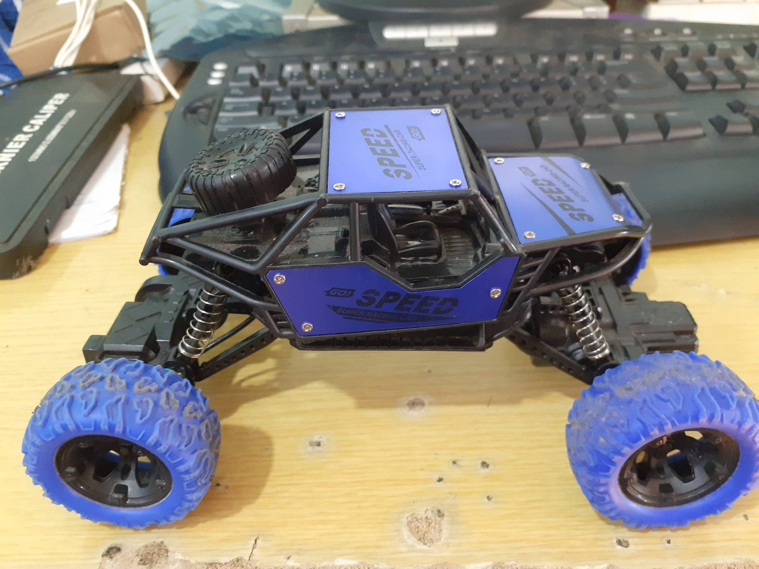
Many of us have old toys laying around the house, they belong to our children or the children of our friends. In this article, I will attempt to show you how to give an old toy car new life, as well as hopefully teach a child a few interesting things with electronics.
The inspiration for this article comes from my friend’s 7-year-old boy, who, way too clever for his age, always has a lot of very interesting questions. His mother and I have thus decided to do an experiment: “Let us try to teach him Arduino programming, so he can start to make his own toys”
Obviously, the challenges in this venture are many… To name a few: The boy speaks only Thai, so English is a no-go. Soldering is out of the question, due to his age, as well as safety issues – All teaching will have to be done on a breadboard.
My challenges apart, this is a project that many people would want to attempt, so it is important to start with a bit of theory.
Controlling a DC Motor from a microcontroller
DC motors, like those found in toy cars, are inductive loads, and that means that they induce electromagnetic fields when switched on or off. These EMF fields can damage your sensitive microcontroller quite easily. Another thing to remember is that your typical microcontroller can only source or sink in the region of 25mA to 50mA of current, not quite enough to drive a motor, let alone a toy car.
Directional control of the motor
In our toy car, we would definitely want the driving motor to be able to change direction, meaning spin forwards or backwards, thereby changing the direction that the car is travelling. This is achieved by using a circuit called an H-Bridge. In this circuit, four transistors, either BJTs or MOSFETs are arranged in a particular way to allow us to change the direction that the motor spins by changing certain logic signals.
Implementing an H-Bridge with switches
In the picture above, we simulate the H-Bridge circuit using slide switches in order to explain the method of operation. It should be clear that the direction is changed by switching on diagonally opposite switches.
Driving a motor with a transistor
In the picture above, we implement a simple, one-directional motor control circuit using a single transistor. This circuit still has the limitation that the motor can only spin in a single direction.
Half of an H-Bridge
In the circuit above, we combine the two motor driver circuits (with PNP and NPN transistor ) to complete one half of the H-Bridge circuit. This circuit still has the limitation that we can only spin the motor in a single direction.
The completed H-Bridge circuit
In the picture above, we added another half H-Bridge to complete the circuit. We will thus have 2 PNP and 2 NPN transistors, which form the completed circuit. This circuit will give us full bi-directional control of the motor. We can also control the speed of the motor if we apply a suitable PWM signal to the bases of the NPN transistors – we do need to be careful of SHOOT THROUGH and shorts though.
My proposed Motor Driving Circuit
the inside of the toy car, without the old broken circuit-board
In the picture above, we can clearly see that there is not a lot going on inside this toy car. An On-Off switch is connected to the battery compartment, and two wires go to the drive- and steering motor.
Interfacing this car to a microcontroller is thus going to require two separate H-Bridge circuits. One for the drive motor, and the second for the steering.
Dual H-Bridge Circuit diagram
I have designed the circuit above to control both motors of the toy car, the control signals are simplified to 2 per H-Bridge, and a common PWM signal to control speed.
Manufacturing the PCB
The PCB for this project is currently on its way from China, after having been manufactured at PCBWay. Please consider supporting them if you would like your own copy of this PCB, or if you have any PCB of your own that you need to be manufactured.
If you would like to have PCBWAY manufacture one of your own, designs, or even this particular PCB, you need to do the following… 1) Click on this link 2) Create an account if you have not already got one of your own. If you use the link above, you will also instantly receive a $5USD coupon, which you can use on your first or any other order later. (Disclaimer: I will earn a small referral fee from PCBWay. This referral fee will not affect the cost of your order, nor will you pay any part thereof.) 3) Once you have gone to their website, and created an account, or login with your existing account,
4) Click on PCB Instant Quote
5) If you do not have any very special requirements for your PCB, click on Quick-order PCB
6) Click on Add Gerber File, and select your Gerber file(s) from your computer. Most of your PCB details will now be automatically selected, leaving you to only select the solder mask and silk-screen colour, as well as to remove the order number or not. You can of course fine-tune everything exactly as you want as well.
7) You can also select whether you want an SMD stencil, or have the board assembled after manufacturing. Please note that the assembly service, as well as the cost of your components, ARE NOT included in the initial quoted price. ( The quote will update depending on what options you select ).
8) When you are happy with the options that you have selected, you can click on the Save to Cart Button. From here on, you can go to the top of the screen, click on Cart, make any payment(s) or use any coupons that you have in your account.
Then just sit back and wait for your new PCB to be delivered to your door via the shipping company that you have selected during checkout.
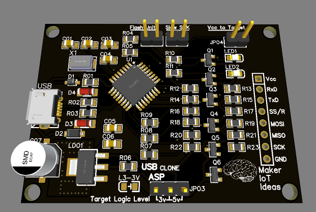
Using more ATMEGA based MCU’s in my recent projects, and not using ready-made Arduino boards for any of them, it became necessary to invest in a dedicated ASP programmer to flash the MCU’s. Huge delays on electronics components, with confirmed orders being mysteriously cancelled due to sourcing issues, and the high cost of “original OEM ASP programmers”, send me on a search for a DIY style programmer, like the old “NOPPP” ( NO PARTS PIC Programmer) in the good old days…
Personal computers have changed a lot, and while ATMEGA chips are not PIC’s, I did feel that it could be done. Given the fact that you could also use an Arduino UNO as an ISP, and doing a little more digging, I finally found a very attractive alternative…
Thomas Fischl, on his website,https://www.fischl.de/usbasp, has an open-source hardware project, that seemed to be exactly what I needed. His device is capable of programming 5v devices, at various speeds, including a super slow one. He has also written firmware for the device, and although the last update was in 2011, It still seems to be working well, or at least as far as I can see…
I did however decide to add my own twist to the design and build in a logic level converter, to be able to program 3.3v devices as well…
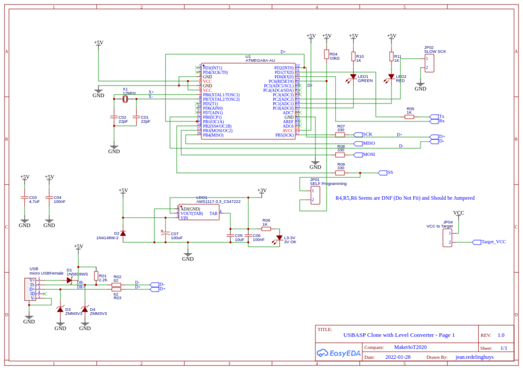
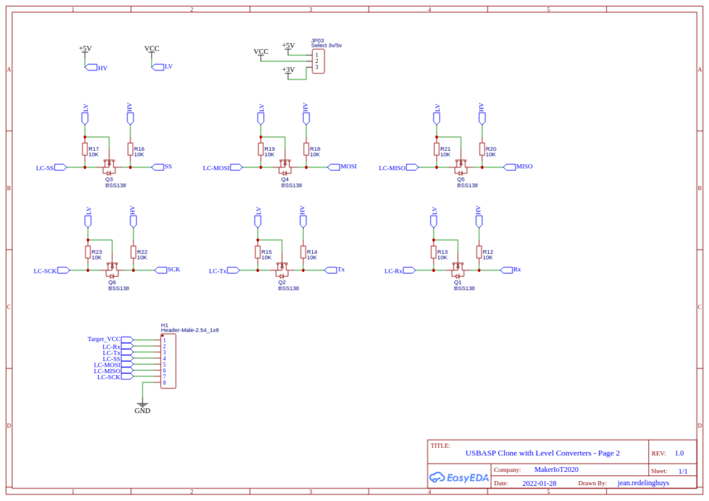
The modified schematic is below:
Schematic Page 1Schematic Page 2
I chose to do my own PCB layout, to incorporate the changes listed earlier, namely the logic level conversion from 5v to 3v, as well as adding a 3.3v LDO voltage regulator to provide 3.3v to the target in case it is required.
PCB TopsidePCB Bottom Side3D Render of the PCB
The PCB is still in transit from the factory, and thus I will update this article later with pictures of the actual device.
Firmware can be flashed using any ASP programmer, Arduino as ISP as well, but with the caveat that you have to use AVRDude from the command line… More on that in the follow-up post… ( I would like to show actual screenshots of the process, and not theory.. ). The links to the firmware are available on https://www.fischl.de/usbasp, courtesy of Thomas Fischl, whom I would like to thank for making this open-source hardware project available freely, as well as for writing and maintaining the firmware.
The PCB can be ordered, or the design files downloaded ( a free download ) from my Projects page at PCBWay soon…
This PCB was manufactured at PCBWAY. The Gerber files and BOM, as well as all the schematics, will soon be available as a shared project on their website. If you would like to have PCBWAY manufacture one of your own, designs, or even this particular PCB, you need to do the following… 1) Click on this link 2) Create an account if you have not already got one of your own. If you use the link above, you will also instantly receive a $5USD coupon, which you can use on your first or any other order later. (Disclaimer: I will earn a small referral fee from PCBWay. This referral fee will not affect the cost of your order, nor will you pay any part thereof.) 3) Once you have gone to their website, and created an account, or login with your existing account,
4) Click on PCB Instant Quote
5) If you do not have any very special requirements for your PCB, click on Quick-order PCB
6) Click on Add Gerber File, and select your Gerber file(s) from your computer. Most of your PCB details will now be automatically selected, leaving you to only select the solder mask and silk-screen colour, as well as to remove the order number or not. You can of course fine-tune everything exactly as you want as well.
7) You can also select whether you want an SMD stencil, or have the board assembled after manufacturing. Please note that the assembly service, as well as the cost of your components, ARE NOT included in the initial quoted price. ( The quote will update depending on what options you select ).
8) When you are happy with the options that you have selected, you can click on the Save to Cart Button. From here on, you can go to the top of the screen, click on Cart, make any payment(s) or use any coupons that you have in your account.
Then just sit back and wait for your new PCB to be delivered to your door via the shipping company that you have selected during checkout.
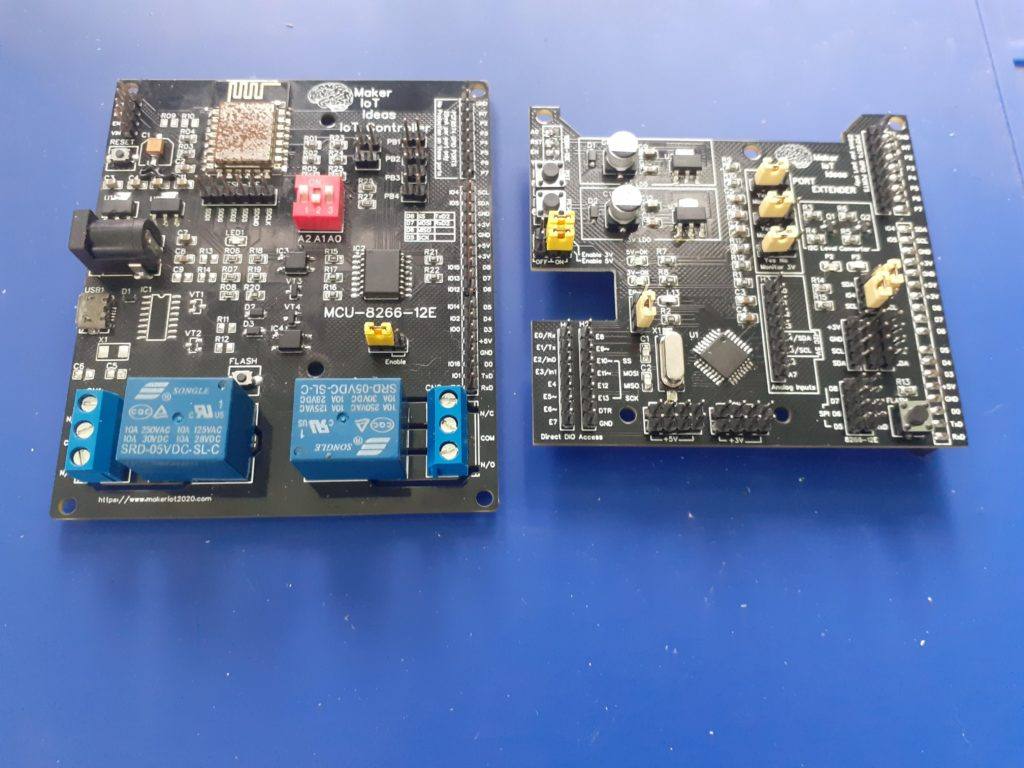
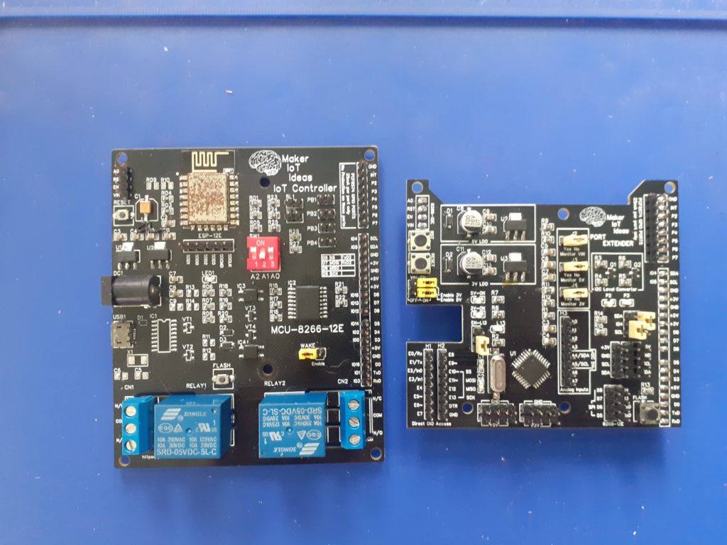
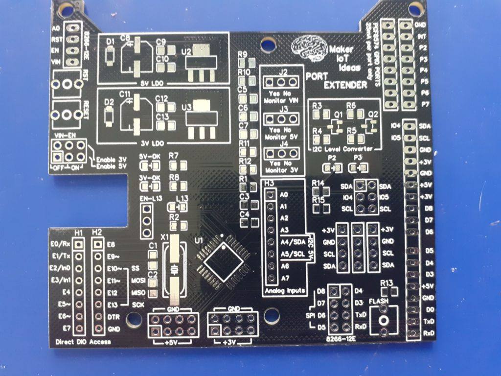
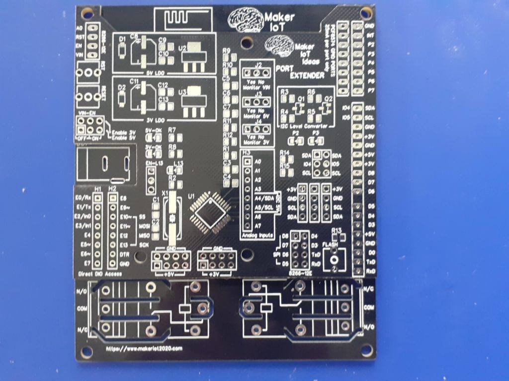
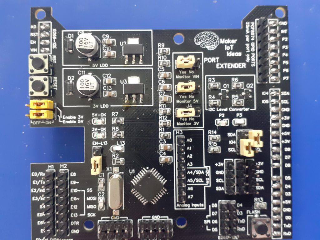
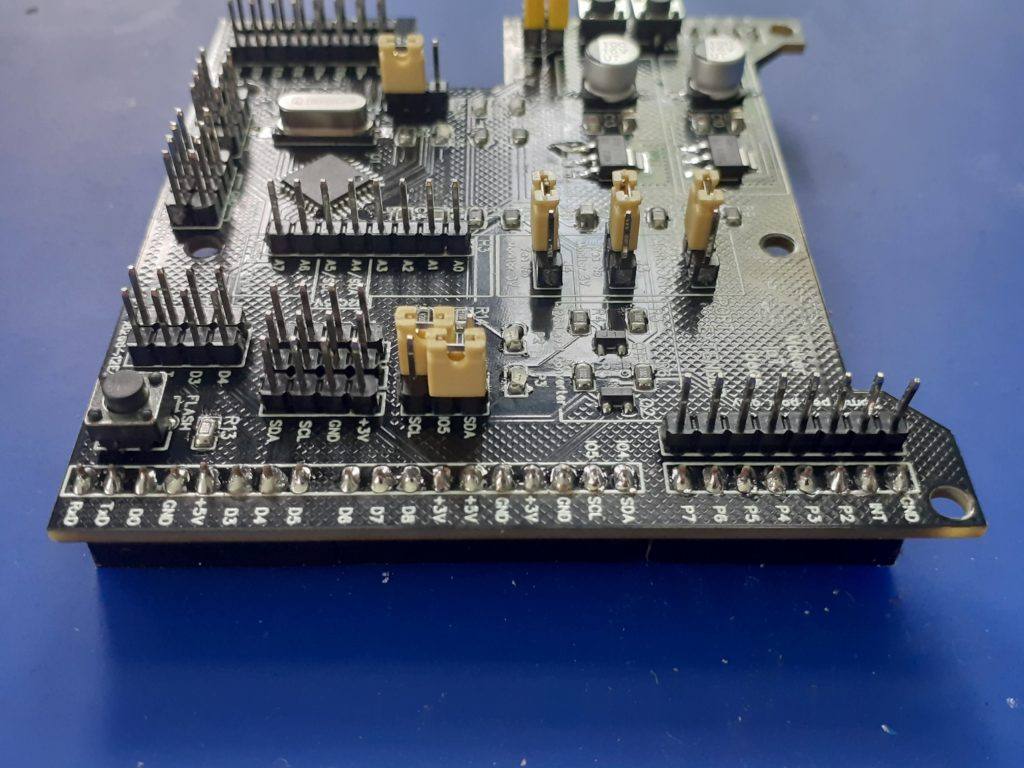
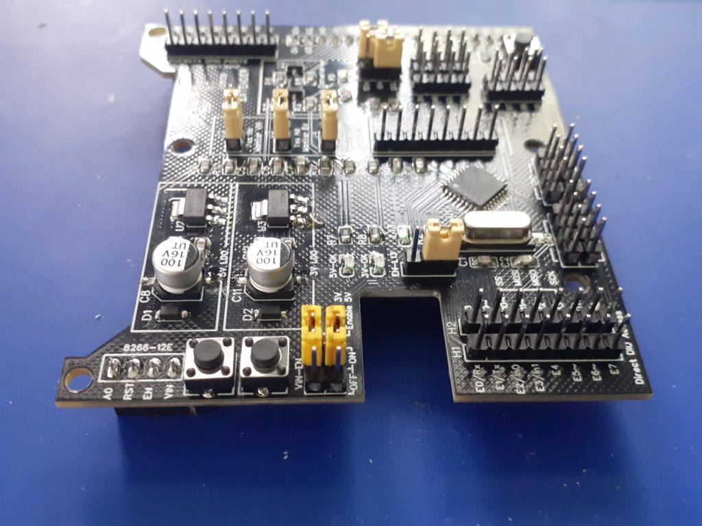
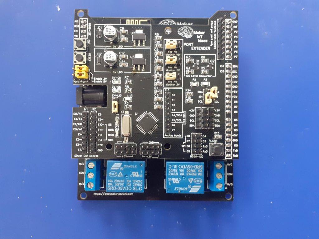
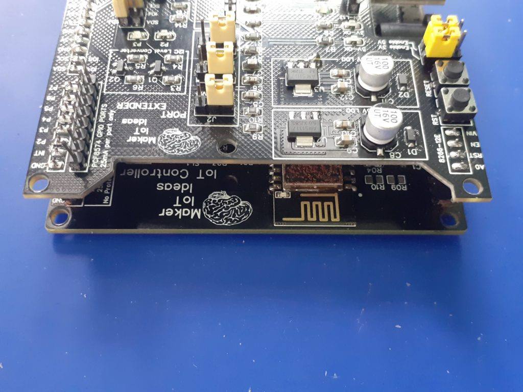
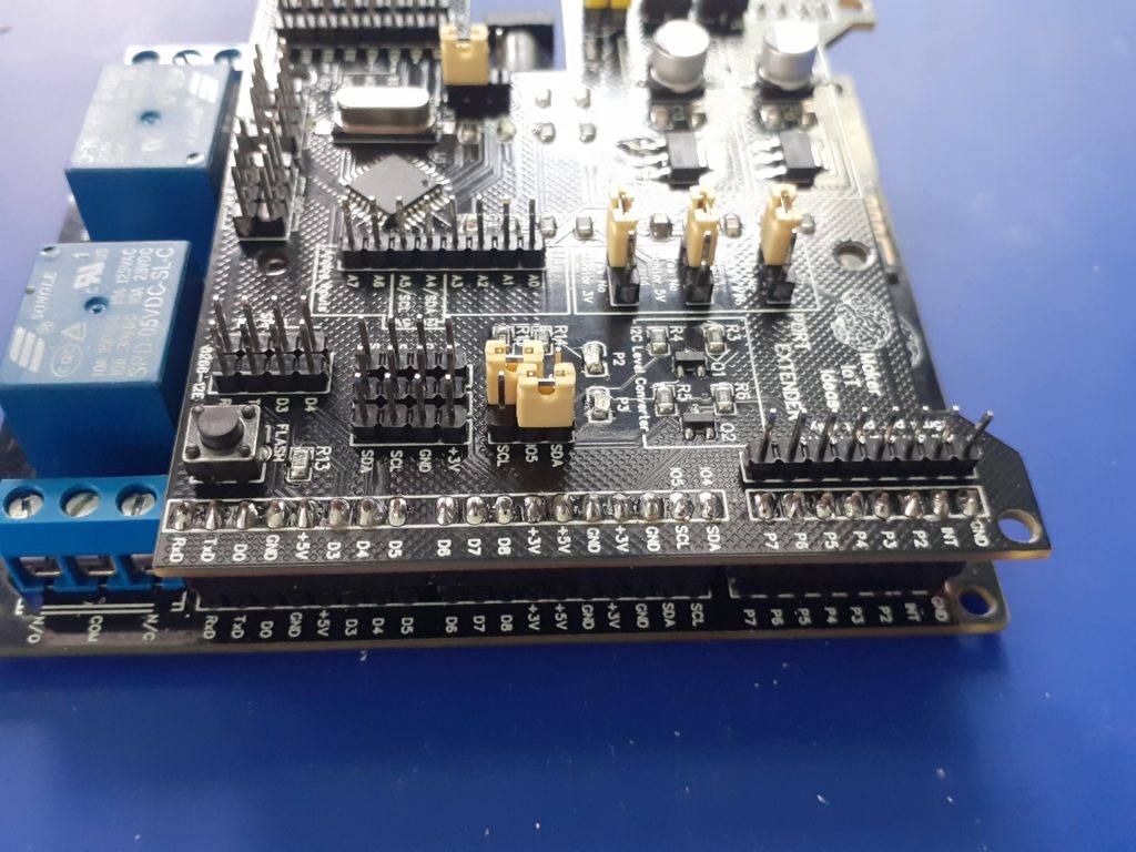
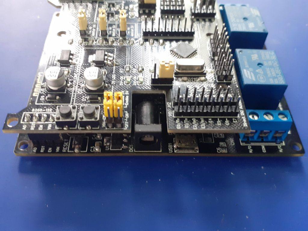
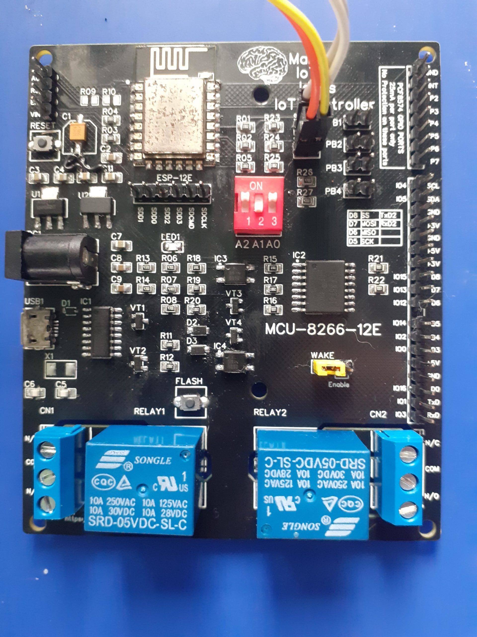
After quite a few experiments, and playing with a lot of ideas, we have finally produced and tested an almost final prototype for the MCU-8266-12E IoT Controller Port Extender Card. While the baseboard already has quite a lot of free GPIO pins for additional sensors and devices, It did however have quite a few issues, namely a lack of sufficient Power outputs, difficulty access to the I2C bus, as well as only 2 relay outputs. Granted that you do have access to unused pins on the PCF8574 Port Extender, We nonetheless decided that an add-on card would definitely make sense to allow this device to really be more useable.
While looking at various ideas for this card, the most flexible seemed to be the APE Protocol device as documented in ESPHome. They used a standard Arduino board for that, but we decided that, after testing it with an Arduino Nano, since it seems to work well, let us just design a dedicated PCB. It also looks much better as well 🙂
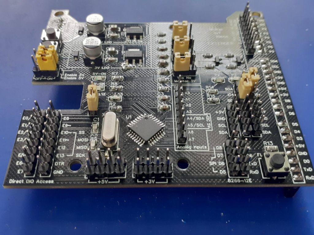
The beginning of the APE (Arduino Port Extender) Device. MCU-8266-12E with Arduino Nano (left) and MCU-8266-12E with the newly designed APE Card (right)
Some Features (Aside from being a fully functional Arduino clone as well)
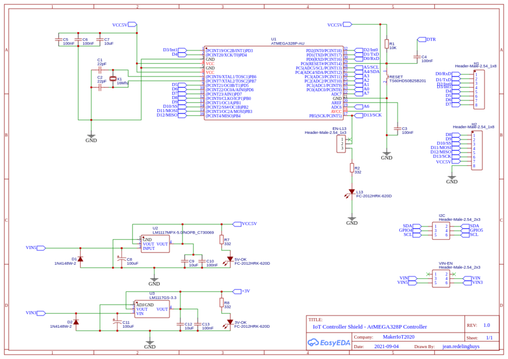
1). Dedicated LDO Regulators for 5v and 3.3v (800mA each), with jumpers to switch them on or off (receive power only from the IoT Motherboard). 2.) Dedicated Logic Level Converter on the I2C Bus ( This is sort of very much needed 🙂 The Atmega 328P-AU is running at 5v on this device, to enable it to run at 16Mhz.. and the ESP8266 on the Motherboard is a 3.3v device..
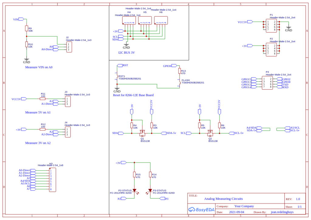
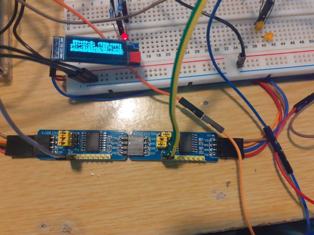
There are also 3x 3.3V I2C Headers, complete with 3.3v and Ground, as well as a single 5v I2C header 3). 8 Analog Inputs ( While practically you can only use 6 of these if you use I2C ) 4). Voltage Divider provided on A0 to measure VIN ( to be safe, we calculated the resistors for 22v) 5). 100R current limiting resistor on A1 and A2, to measure 5v and 3.3v as well… Analog inputs A0, A1 and A2 can be switched back to normal operation by changing the jumper at J2,J3 or J4 from On to Off. 6). 12 Digital Inputs/Outputs (14 if you use D0 and D1 as well), as well as a Jumper to remove the LED on D13. 7). Full access to the PCF8574 and ESP8266 Pins from the motherboard below.
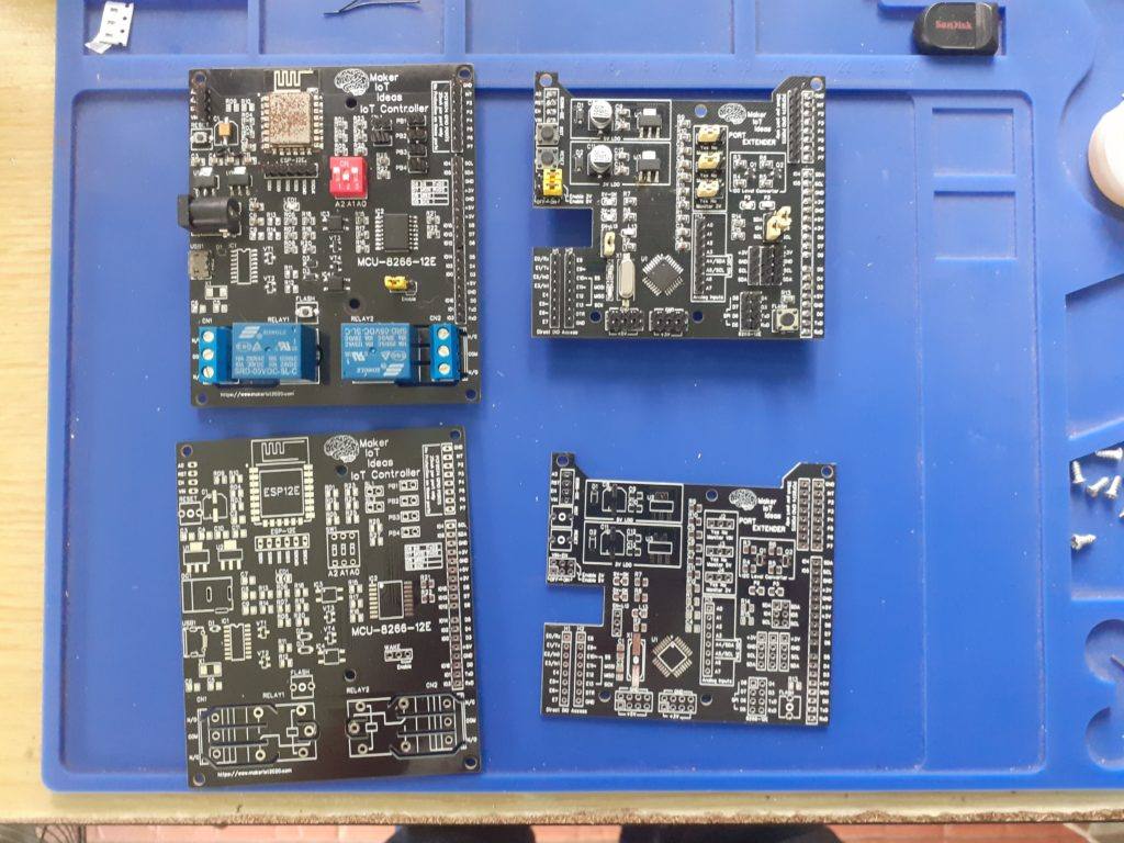
Pictures of the PCB
Side by side MCU-8266-12E (left) 8266-12E-Port Extender (right)
Side by side MCU-8266-12E (left) 8266-12E-Port Extender (right)
Side by side MCU-8266-12E (left) 8266-12E-Port Extender (right) [ with unpopulated PCB at bottom]
Blank PCB 8266-12E-Port Extender
Blank PCB MCU-8266-12E IoT Controller
Top view 8266-12E PE
8266-12E-PE side view { from bottom)
Right side view – 8266-12E-PE
Left side view – 8266-12E-PE
Stacked on-top-of MCU-8266-12E
Stacked – Top Side view
Stacked – Right side view
Stacked – Left side view
Pictures of the PCB, alone and with the MCU-8266-12E IoT controller
Circuit Diagram
ATMega328P-AU Circuit diagram with LDO Regulators, headers and supporting circuitry.Analog measuring circuitry, level converters and supporting circuitry and headers
Uploading Code to the ATMega328P
Uploading code to the device requires the use of either an ISCP programmer ( Arduino as ISP works well ) or in the case of a pre-boot loaded chip, a USB-to-Serial converter. We did not find it necessary to add a dedicated USB-to-Serial converter onto the PCB. It is quite easy enough to do any flashing with the tools mentioned above.
Make sure that the PCB is not stacked when doing this. ( This will prevent excessive current use of other components when you supply 5v to the PE card.
Procedure to upload using ICSP
During assembly, you are required to solder a single 90-degree bend pin header on the bottom side of the PCB, in the same hole as the board side edge of the RESET push-button. This will serve as the RESET Pin for the ISCP. Other connections are as follows:
H2 Header <- > ICSP Programmer MOSI (E11~) – MOSI ( or Pin 11 on Arduino as ISP ) MISO (E12 ) – MISO ( or Pin 12 on Arduino as ISP ) SCK (E13) – D13 (or Pin 13 on Arduino as ISP ) RESET – D10 (or Pin 10 on Arduino as ISP )
5v and Ground from Arduino as ISP or ISCP Programmer to any 5v and ground pin on the PE Card
Please note the description above for assembly of the RESET pin header
Procedure to upload using USB-to-Serial converter
H1 Header
E0/Rx <- to Tx of USB-to-Serial converter E1/Tx -> to Rx of USB-to-Serial converter
H2 Header
DTR <-> to DTR of USB-to-Serial converter [ This connection is needed for successful uploading. Don’t leave it out ]
5v and Ground from the USB-to-Serial converter to any 5v and ground pin on the PE Card
Testing with ESPHome APE protocol and the MCU-8266-12E IoT controller
The following Arduino Sketch needs to be uploaded to the device. It will allow the device to function as a custom I2C device. Feel free to change the I2C address in the sketch as you choose, but remember to use the same address in your ESPHome YAML configuration file
The following C header file needs to be uploaded to your Home Assistant ESPHome folder.
// Must disable logging if using logging in main.cpp or in other custom components for the
//  __c causes a section type conflict with __c thingy
// you can enable logging and use it if you enable this in logger:
/*
logger:
  level: DEBUG
  esp8266_store_log_strings_in_flash: False
  */

//#define APE_LOGGING

// take advantage of LOG_ defines to decide which code to include
#ifdef LOG_BINARY_OUTPUT
#define APE_BINARY_OUTPUT
#endif
#ifdef LOG_BINARY_SENSOR
#define APE_BINARY_SENSOR
#endif
#ifdef LOG_SENSOR
#define APE_SENSOR
#endif

static const char *TAGape = "ape";

#define APE_CMD_DIGITAL_READ 0
#define APE_CMD_WRITE_ANALOG 2
#define APE_CMD_WRITE_DIGITAL_HIGH 3
#define APE_CMD_WRITE_DIGITAL_LOW 4
#define APE_CMD_SETUP_PIN_OUTPUT 5
#define APE_CMD_SETUP_PIN_INPUT_PULLUP 6
#define APE_CMD_SETUP_PIN_INPUT 7
// 8 analog registers.. A0 to A7
// A4 and A5 not supported due to I2C
#define CMD_ANALOG_READ_A0 0b1000 // 0x8
// ....
#define CMD_ANALOG_READ_A7 0b1111 // 0xF

#define CMD_SETUP_ANALOG_INTERNAL 0x10
#define CMD_SETUP_ANALOG_DEFAULT 0x11

#define get_ape(constructor) static_cast<ArduinoPortExpander *>(constructor.get_component(0))

#define ape_binary_output(ape, pin) get_ape(ape)->get_binary_output(pin)
#define ape_binary_sensor(ape, pin) get_ape(ape)->get_binary_sensor(pin)
#define ape_analog_input(ape, pin) get_ape(ape)->get_analog_input(pin)

class ArduinoPortExpander;

using namespace esphome;

#ifdef APE_BINARY_OUTPUT
class ApeBinaryOutput : public output::BinaryOutput
{
public:
  ApeBinaryOutput(ArduinoPortExpander *parent, uint8_t pin)
  {
    this->parent_ = parent;
    this->pin_ = pin;
  }
  void write_state(bool state) override;
  uint8_t get_pin() { return this->pin_; }

protected:
  ArduinoPortExpander *parent_;
  uint8_t pin_;
  // Pins are setup as output after the state is written, Arduino has no open drain outputs, after setting an output it will either sink or source thus activating outputs writen to false during a flick.
  bool setup_{true};
  bool state_{false};

  friend class ArduinoPortExpander;
};
#endif

#ifdef APE_BINARY_SENSOR
class ApeBinarySensor : public binary_sensor::BinarySensor
{
public:
  ApeBinarySensor(ArduinoPortExpander *parent, uint8_t pin)
  {
    this->pin_ = pin;
  }
  uint8_t get_pin() { return this->pin_; }

protected:
  uint8_t pin_;
};
#endif

#ifdef APE_SENSOR
class ApeAnalogInput : public sensor::Sensor
{
public:
  ApeAnalogInput(ArduinoPortExpander *parent, uint8_t pin)
  {
    this->pin_ = pin;
  }
  uint8_t get_pin() { return this->pin_; }

protected:
  uint8_t pin_;
};
#endif

class ArduinoPortExpander : public Component, public I2CDevice
{
public:
  ArduinoPortExpander(I2CBus *bus, uint8_t address, bool vref_default = false)
  {
    set_i2c_address(address);
    set_i2c_bus(bus);
    this->vref_default_ = vref_default;
  }
  void setup() override
  {
#ifdef APE_LOGGING
    ESP_LOGCONFIG(TAGape, "Setting up ArduinoPortExpander at %#02x ...", address_);
#endif

    /* We cannot setup as usual as arduino boots later than esp8266
            Poll i2c bus for our Arduino for a n seconds instead of failing fast,
            also this is important as pin setup (INPUT_PULLUP, OUTPUT it's done once)
        */
    this->configure_timeout_ = millis() + 5000;
  }
  void loop() override
  {
    if (millis() < this->configure_timeout_)
    {
      bool try_configure = millis() % 100 > 50;
      if (try_configure == this->configure_)
        return;
      this->configure_ = try_configure;

      if (ERROR_OK == this->read_register(APE_CMD_DIGITAL_READ, const_cast<uint8_t *>(this->read_buffer_), 3))
      {
#ifdef APE_LOGGING
        ESP_LOGCONFIG(TAGape, "ArduinoPortExpander found at %#02x", address_);
#endif
        delay(10);
        if (this->vref_default_)
        {
          this->write_register(CMD_SETUP_ANALOG_DEFAULT, nullptr, 0); // 0: unused
        }

        // Config success
        this->configure_timeout_ = 0;
        this->status_clear_error();
#ifdef APE_BINARY_SENSOR
        for (ApeBinarySensor *pin : this->input_pins_)
        {
          App.feed_wdt();
          uint8_t pinNo = pin->get_pin();
#ifdef APE_LOGGING
          ESP_LOGCONFIG(TAGape, "Setup input pin %d", pinNo);
#endif
          this->write_register(APE_CMD_SETUP_PIN_INPUT_PULLUP, &pinNo, 1);
          delay(20);
        }
#endif
#ifdef APE_BINARY_OUTPUT
        for (ApeBinaryOutput *output : this->output_pins_)
        {
          if (!output->setup_)
          { // this output has a valid value already
            this->write_state(output->pin_, output->state_, true);
            App.feed_wdt();
            delay(20);
          }
        }
#endif
#ifdef APE_SENSOR
        for (ApeAnalogInput *sensor : this->analog_pins_)
        {
          App.feed_wdt();
          uint8_t pinNo = sensor->get_pin();
#ifdef APE_LOGGING
          ESP_LOGCONFIG(TAGape, "Setup analog input pin %d", pinNo);
#endif
          this->write_register(APE_CMD_SETUP_PIN_INPUT, &pinNo, 1);
          delay(20);
        }
#endif
        return;
      }
      // Still not answering
      return;
    }
    if (this->configure_timeout_ != 0 && millis() > this->configure_timeout_)
    {
#ifdef APE_LOGGING
      ESP_LOGE(TAGape, "ArduinoPortExpander NOT found at %#02x", address_);
#endif
      this->mark_failed();
      return;
    }

#ifdef APE_BINARY_SENSOR
    if (ERROR_OK != this->read_register(APE_CMD_DIGITAL_READ, const_cast<uint8_t *>(this->read_buffer_), 3))
    {
#ifdef APE_LOGGING
      ESP_LOGE(TAGape, "Error reading. Reconfiguring pending.");
#endif
      this->status_set_error();
      this->configure_timeout_ = millis() + 5000;
      return;
    }
    for (ApeBinarySensor *pin : this->input_pins_)
    {
      uint8_t pinNo = pin->get_pin();

      uint8_t bit = pinNo % 8;
      uint8_t value = pinNo < 8 ? this->read_buffer_[0] : pinNo < 16 ? this->read_buffer_[1] : this->read_buffer_[2];
      bool ret = value & (1 << bit);
      if (this->initial_state_)
        pin->publish_initial_state(ret);
      else
        pin->publish_state(ret);
    }
#endif
#ifdef APE_SENSOR
    for (ApeAnalogInput *pin : this->analog_pins_)
    {
      uint8_t pinNo = pin->get_pin();
      pin->publish_state(analogRead(pinNo));
    }
#endif
    this->initial_state_ = false;
  }

#ifdef APE_SENSOR
  uint16_t analogRead(uint8_t pin)
  {
    bool ok = (ERROR_OK == this->read_register((uint8_t)(CMD_ANALOG_READ_A0 + pin), const_cast<uint8_t *>(this->read_buffer_), 2));
#ifdef APE_LOGGING
    ESP_LOGVV(TAGape, "analog read pin: %d ok: %d byte0: %d byte1: %d", pin, ok, this->read_buffer_[0], this->read_buffer_[1]);
#endif
    uint16_t value = this->read_buffer_[0] | ((uint16_t)this->read_buffer_[1] << 8);
    return value;
  }
#endif

#ifdef APE_BINARY_OUTPUT
  output::BinaryOutput *get_binary_output(uint8_t pin)
  {
    ApeBinaryOutput *output = new ApeBinaryOutput(this, pin);
    output_pins_.push_back(output);
    return output;
  }
#endif
#ifdef APE_BINARY_SENSOR
  binary_sensor::BinarySensor *get_binary_sensor(uint8_t pin)
  {
    ApeBinarySensor *binarySensor = new ApeBinarySensor(this, pin);
    input_pins_.push_back(binarySensor);
    return binarySensor;
  }
#endif
#ifdef APE_SENSOR
  sensor::Sensor *get_analog_input(uint8_t pin)
  {
    ApeAnalogInput *input = new ApeAnalogInput(this, pin);
    analog_pins_.push_back(input);
    return input;
  }
#endif
  void write_state(uint8_t pin, bool state, bool setup = false)
  {
    if (this->configure_timeout_ != 0)
      return;
#ifdef APE_LOGGING
    ESP_LOGD(TAGape, "Writing %d to pin %d", state, pin);
#endif
    this->write_register(state ? APE_CMD_WRITE_DIGITAL_HIGH : APE_CMD_WRITE_DIGITAL_LOW, &pin, 1);
    if (setup)
    {
      App.feed_wdt();
      delay(20);
#ifdef APE_LOGGING
      ESP_LOGI(TAGape, "Setup output pin %d", pin);
#endif
      this->write_register(APE_CMD_SETUP_PIN_OUTPUT, &pin, 1);
    }
  }

protected:
  bool configure_{true};
  bool initial_state_{true};
  uint8_t read_buffer_[3]{0, 0, 0};
  unsigned long configure_timeout_{5000};
  bool vref_default_{false};

#ifdef APE_BINARY_OUTPUT
  std::vector<ApeBinaryOutput *> output_pins_;
#endif
#ifdef APE_BINARY_SENSOR
  std::vector<ApeBinarySensor *> input_pins_;
#endif
#ifdef APE_SENSOR
  std::vector<ApeAnalogInput *> analog_pins_;
#endif
};

#ifdef APE_BINARY_OUTPUT
void ApeBinaryOutput::write_state(bool state)
{
  this->state_ = state;
  this->parent_->write_state(this->pin_, state, this->setup_);
  this->setup_ = false;
}
#endif
The file should be named “arduino_port_expander.h”
Make the following changes to your ESPHome YAML configuration file for the MCU-8266-12E device
esphome:
  name: mcu-8266-12e-01
  platform: ESP8266
  board: nodemcuv2
  includes:
      - arduino_port_expander.h
# Note the include file - This loads the APE Header

# Enable logging
logger:

# Enable Home Assistant API
api:

ota:
  password: "<your password will be different - dont change it>"

wifi:
  ssid: <your ssid>
  password: <your password>

  # Enable fallback hotspot (captive portal) in case wifi connection fails
  ap:
    ssid: "MCU-8266-Hotspot"
    password: "password"

captive_portal:

i2c:
# PCB Prototype
  sda: GPIO5
  scl: GPIO4
# PCB Rev 1.5 or higher, comment the above 2 lines
# and uncomment
#sda: GPIO4
#scl: GPIO5
#################### - IMPORTANT ###########
  scan: true
  id: i2c_bus_a

pcf8574:
  - id: 'pcf8574_hub'
    address: 0x22 # Set at 0x22, feel free to change to your liking, Remember to set the chip to the address you choose as well
    pcf8575: false

time:
  - platform: sntp
    id: ha_time
    timezone: "Etc/GMT+7"

status_led:
  pin:
    number: GPIO16
    inverted: true

#Define the APE as a custom component, taking care to ensure that:
#1). The I2C Bust ID is the same as the one you have defined in the I2C: Section
#2). The address of the APE is the same as the one you set in the sketch

custom_component:
  - id: ape
    lambda: |-
      auto ape_component = new ArduinoPortExpander(i2c_bus_a, 0x08,true);
      return {ape_component};


sensor:

  - platform: custom
    lambda: |-
      return {ape_analog_input(ape, 0),  // 1 = A1
             ape_analog_input(ape, 1),
             ape_analog_input(ape, 2)};

#We define 3 analog inputs (A0,A1,A2) to monitor voltages on the card
#Note that you MUST define them in the sensors section below as well AND
#THAT THEY MUST BE IN THE SAME SEQUENCE THAT YOU DEFINED THEM IN ABOVE HERE
#
#ALSO NOTE THAT YOU CAN "NOT" use A4 and A5, as they are used for I2C !
#
# As an example, of adding another 3 analog inputs, your definition above will change to:
#
#    return {ape_analog_input(ape, 0),
#           ape_analog_input(ape, 1),
#           ape_analog_input(ape, 2),
#           ape_analog_input(ape, 3),
#           ape_analog_input(ape, 6),
#           ape_analog_input(ape, 7)};
#
#
# Now define the sensors connected to these analogs below:


    sensors:
      - name: "PE Card VIN"
        id: analog_a0
        device_class: "voltage"
        unit_of_measurement: "v"
        accuracy_decimals: 2
        filters:
          - lambda: return x * (22.00/1023.0);
          - throttle: 60s

# We use a lambda to scale the value of VIN - Our Voltage divider was designed around 22 volt
# thus we need 22 volt here in the calculation as well to make it accurate
#
      - name: "PE Card 5v"
        id: analog_a1
        device_class: "voltage"
        unit_of_measurement: "v"
        accuracy_decimals: 2
        filters:
          - lambda: return x * (5.02/1023.0);
          - throttle: 60s
      - name: "PE Card 3v"
        id: analog_a2
        device_class: "voltage"
        unit_of_measurement: "v"
        accuracy_decimals: 2
        filters:
          - lambda: return x * (5.02/1023.0);
          - throttle: 60s

# The ATMega328P 's Analog Reference is set to 5v internally, thus we need to also scale the
# 3v input with a maximum of 5v ...

# In case you enabled the other 3 Analog Inputs above, you need to add the following
#
#    - name: "Analog 3"
#      id: analog_a3
#      filters:
#        - throttle: 60s
#    - name: "Analog 6"
#      id: analog_a6
#      filters:
#        - throttle: 60s
#    - name: "Analog 7"
#      id: analog_a7
#      filters:
#        - throttle: 60s
#
#


  - platform: adc
    pin: VCC
    name: "ESP8266 Chip Voltage"
    id: mcu_voltage
    unit_of_measurement: "V"
    device_class: "voltage"
    accuracy_decimals: 2
    update_interval: 60s

  - platform: wifi_signal
    name: "WiFi Signal Sensor"
    id: wifi_strength
    device_class: "signal_strength"
    unit_of_measurement: "dBm"
    update_interval: 240s


#Digital outputs function the same

output:
- platform: custom
  type: binary
  lambda: |-
    return {ape_binary_output(ape, 2),
            ape_binary_output(ape, 3),
            ape_binary_output(ape, 4),
            ape_binary_output(ape, 5),
            ape_binary_output(ape, 6),
            ape_binary_output(ape, 7)};
  outputs:
    - id: ape_output_p2
      inverted: false
    - id: ape_output_p3
      inverted: false
    - id: ape_output_p4
      inverted: false
    - id: ape_output_p5
      inverted: false
    - id: ape_output_p6
      inverted: false
    - id: ape_output_p7
      inverted: false

- platform: gpio
  id: relay_1
  pin:
    pcf8574: pcf8574_hub
    number: 0
    mode: OUTPUT
    inverted: true
- platform: gpio
  id: relay_2
  pin:
    pcf8574: pcf8574_hub
    number: 1
    mode: OUTPUT
    inverted: true
- platform: gpio
  id: led_status_1
  pin:
    pcf8574: pcf8574_hub
    number: 2
    mode: OUTPUT
    inverted: true
- platform: gpio
  id: led_status_2
  pin:
    pcf8574: pcf8574_hub
    number: 3
    mode: OUTPUT
    inverted: true

binary_sensor:
  - platform: gpio
    id: push_button_1
    name: 'Relay1 Pushbutton'
    device_class: ''
    pin:
      pcf8574: pcf8574_hub
      number: 4
      mode: INPUT
      inverted: true
    on_press:
      then:
        - switch.toggle: switch_relay1

  - platform: gpio
    id: push_button_2
    name: 'Relay2 Pushbutton'
    device_class: ''
    pin:
      pcf8574: pcf8574_hub
      number: 5
      mode: INPUT
      inverted: true
    on_press:
      #min_length: 50ms
      #max_length: 500ms
      then:
        - switch.toggle: switch_relay2
    filters:
        - delayed_on_off: 50ms


switch:
  - platform: output
    id: switch_relay1
    name: "Relay No. 1 (#0)"
    output: relay_1
    on_turn_on:
      - output.turn_on: led_status_1
    on_turn_off:
      - output.turn_off: led_status_1

  - platform: output
    id: switch_relay2
    name: "Relay No. 2 (#1)"
    output: relay_2
    on_turn_on:
      - output.turn_on: led_status_2
    on_turn_off:
      - output.turn_off: led_status_2
  - platform: restart
    id: reboot_switch
    name: "Reboot Me"
This PCB was manufactured at PCBWAY. The Gerber files and BOM, as well as all the schematics, will soon be available as a shared project on their website. If you would like to have PCBWAY manufacture one of your own, designs, or even this particular PCB, you need to do the following… 1) Click on this link 2) Create an account if you have not already got one of your own. If you use the link above, you will also instantly receive a $5USD coupon, which you can use on your first or any other order later. (Disclaimer: I will earn a small referral fee from PCBWay. This referral fee will not affect the cost of your order, nor will you pay any part thereof.) 3) Once you have gone to their website, and created an account, or login with your existing account,
4) Click on PCB Instant Quote
5) If you do not have any very special requirements for your PCB, click on Quick-order PCB
6) Click on Add Gerber File, and select your Gerber file(s) from your computer. Most of your PCB details will now be automatically selected, leaving you to only select the solder mask and silk-screen colour, as well as to remove the order number or not. You can of course fine-tune everything exactly as you want as well.
7) You can also select whether you want an SMD stencil, or have the board assembled after manufacturing. Please note that the assembly service, as well as the cost of your components, ARE NOT included in the initial quoted price. ( The quote will update depending on what options you select ).
8) When you are happy with the options that you have selected, you can click on the Save to Cart Button. From here on, you can go to the top of the screen, click on Cart, make any payment(s) or use any coupons that you have in your account.
Then just sit back and wait for your new PCB to be delivered to your door via the shipping company that you have selected during checkout.
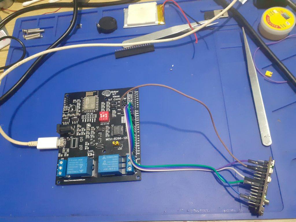
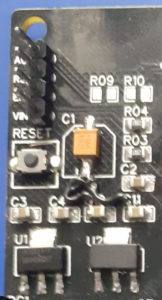
Welcome to Part 3 of this build. If you are new to this series, Part1 and Part2 can be found by clicking on the respective links. Today, we will look at the completed PCB for our IoT Controller. Full disclosure, There are some issues, ranging from components that have still (15 days after being ordered, not been delivered), as well as 3 minor errors on the PCB ( That is entirely my fault ). We will look at how I have overcome the problems to still end up with a functionals PCB. Please note that the errors in the PCB Artwork have BEEN CORRECTED and that the version for public download does not contain any errors. You can thus order it with confidence.
During the design phase, I have forgotten to add a ground to the 5v regulator, and its supporting smoothing capacitors. These components were not initially included in my design, but, while added in later after I decided that since I will be designing the PCB to operate from many different voltage inputs, a reliable 5v source that is not dependent on USB power should be added… The components were added to the schematic, and I forgot to add the ground. It went undetected on the PCB design, as the Ground plane is a copper area…
In the picture above, you can see that I have temporarily fixed it with two wire links from the ground of C1, to the grounds of C10 and C11 respectively. These grounds connect back to U2.
C1 is another issue. Originally designed as a 100uf Electrolytic capacitor, I had to settle for a 10uf Tantalum. The reason being that the ordered capacitors are still floating in logistics space… with no definite ETA.
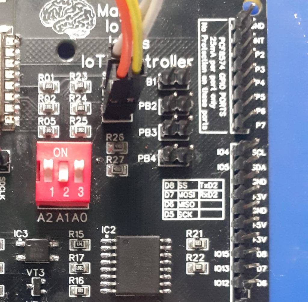
Error on I2C labelling, as well as I2C Pins at IC2
The following error was not so easy to spot. It gave me quite a headache to find. As I normally use netlabels on all the pins of any IC that I use, I have correctly labelled ESP12-E GPIO5 as SCL and GPIO4 as SDA. These netlabels were then transferred onto the PFC8574’s pins but in reverse! Note to self: Always re-read the pinout in the datasheet! To make matters worse, I flipped the SCL and SDA labels on the pin header…
How to fix: I am fortunate that the ESP12-E, like all other ESP Modules, does not have fixed I2C pins. If this was an Atmega based project, the boards would have been useless if tracks could not be cut and reconnected! On the ESP12-E, I2C is however software allocated to any desired GPIO pin. It was thus easily fixed by just swapping the two pins in software.
The third problem encountered is another logistics issue. This is in the process of being resolved, but, as you will soon see, is not actually a problem at all…
I have added support for an onboard USB to Serial converter, via a CH340G chip. The chip requires a 12Mhz resonator or crystal. My dear supplier accidentally sent me an 8 Mhz version. I have thus decided to depopulate the entire USB to Serial circuit, leaving just the USB Port and protection diode on the board. (To allow for powering via USB).
This does mean that programming the board becomes a little more complicated, connecting an external USB to Serial Adapter, and pressing and holding the flash button while pressing and releasing reset for each upload, followed by a manual reset afterwards. This is a pain, but, as I will be using these boards with ESPHome, only required once. All future uploads will be OTA anyway, and the correct components can be retrofitted when they arrive at a later stage.
Powering on the PCB
The PCB was first powered on with an external USB to serial converter and using the Arduino IDE, a simple sketch testing the I2C addressing of the chip, as well as the functioning of all onboard relays and LEDs.
The board was then flashed with ESPHome, using the procedure described in Part 1. I then proceeded to measure the current required by the board, to make sure that it is as designed.
Current Requirements Powered from 9V to 12V DC via the DC Barrel Connector
Standby, Wifi Connected to Home Assistant, All relays and LEDs off 75mA All relays energised, status LEDs all on 255mA
Integrating and Testing with EspHome and Home Assistant
The configuration for ESPHome was updated and uploaded to the device OTA. I decided to add a monitor for the VCC input of the ESP12-E, a remote Restart button, and an external DHT11 Temperature and Humidity sensor. The updated code is available below
esphome:
  name: iot-controller-8266-01
  platform: ESP8266
  board: nodemcuv2

# Enable logging
logger:

# Enable Home Assistant API
api:

ota:
  password: "2f8a73f47f1893f3f7baa391c4d0ba96"

wifi:
  ssid: "<your ssid>"
  password: "<your password>"

  # Enable fallback hotspot (captive portal) in case wifi connection fails
  ap:
    ssid: "Iot-Controller-8266-01"
    password: "y4aaH7vMITsC"

captive_portal:
#--- DO NOT COPY ANYTHING ABOVE THIS LINE ---

# when using this, you need to reassign the status LED to another GPIO
#deep_sleep:
#  run_duration: 5min
#  sleep_duration: 2min

i2c:
  sda: GPIO5
  scl: GPIO4
  scan: true
  id: i2c_bus_a

pcf8574:
  - id: 'pcf8574_hub'
    address: 0x22
    pcf8575: false

status_led:
    pin:
      number: GPIO16
      inverted: true
# Reassign this LED to another GPIO when using deep sleep mode !

sensor:
# Monitor VCC on the ESP12-E
  - platform: adc
    pin: VCC
    name: "Device Input Voltage"
    unit_of_measurement: "V"
# Monitor the WiFi Signal Strength at the device
  - platform: wifi_signal
    name: "WiFi Signal Sensor"
    unit_of_measurement: "dBm"
    update_interval: 240s
# Add Temperature and Humidity Sensor
  - platform: dht
    pin: GPIO2
    temperature:
      name: "Room Temperature"
      unit_of_measurement: "°C"
      icon: "mdi:temperature"
      device_class: "temperature"
      state_class: "measurement"
      accuracy_decimals: 2

    humidity:
      name: "Room Humidity"
      unit_of_measurement: "%"
      icon: "mdi:water-percent"
      device_class: "humidity"
      state_class: "measurement"
      accuracy_decimals: 2
    update_interval: 60s

# Outputs to control relays and led's

output:
 - platform: gpio
   id: relay_1
   pin:
      pcf8574: pcf8574_hub
      number: 0
      mode: OUTPUT
      inverted: true
 - platform: gpio
   id: relay_2
   pin:
      pcf8574: pcf8574_hub
      number: 1
      mode: OUTPUT
      inverted: true
 - platform: gpio
   id: led_status_1
   pin:
      pcf8574: pcf8574_hub
      number: 2
      mode: OUTPUT
      inverted: true
 - platform: gpio
   id: led_status_2
   pin:
      pcf8574: pcf8574_hub
      number: 3
      mode: OUTPUT
      inverted: true
# Monitor the two local control pushbuttons on the device
binary_sensor:
  -  platform: gpio
     id: push_button_1
     name: 'Relay1 Pushbutton'
     device_class: ''
     pin:
        pcf8574:  pcf8574_hub
        number: 4
        mode: INPUT
        inverted: true
     on_press:
      then:
        - switch.toggle: switch_relay1
     filters:
       -  delayed_on_off: 50ms

  -  platform: gpio
     id: push_button_2
     name: 'Relay2 Pushbutton'
     device_class: ''
     pin:
        pcf8574:  pcf8574_hub
        number: 5
        mode: INPUT
        inverted: true
     on_press:
      #min_length: 50ms
      #max_length: 500ms
      then:
        - switch.toggle: switch_relay2
     filters:
       -  delayed_on_off: 50ms

# Allow control from inside Home Assistant

switch:
  - platform: output
    id: switch_relay1
    name: "Relay No. 1 (#0)"
    output: relay_1
    on_turn_on:
    - output.turn_on: led_status_1
    on_turn_off:
    - output.turn_off: led_status_1
  - platform: output
    id: switch_relay2
    name: "Relay No. 2 (#1)"
    output: relay_2
    on_turn_on:
    - output.turn_on: led_status_2
    on_turn_off:
    - output.turn_off: led_status_2
 # Add a remote Reboot switch
  - platform: restart
    name: "Reboot Me"
After uploading this configuration, Home Assistant was configured to reflect the changes.
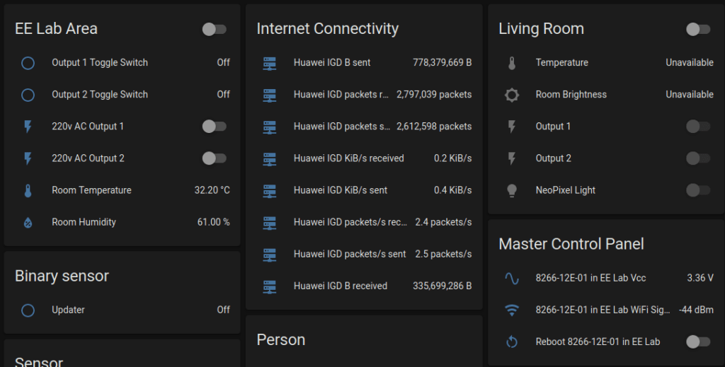
Home Assistant showing the IoT Controller status ( EE Lab Area ) as well as Admin stats (Master Control Panel)
I have decided to split the different status and control outputs from the device into two cards, One in the EE Lab Area, which will later be moved into the actual room(s) where the device will be deployed, as well as on a Master Control Panel. From here, I can reboot individual devices, see their voltages and WiFi Status
Tasmota
As promised before, I did test the device with Tasmota. I had to do a custom compile to get support for the PCF8574. Performance was however VERY poor. ESPHome is snappy and quick, even in local mode. Tasmota seemed to have at least a one-second delay on doing anything. I thus abandoned it, and won’t be making use of it in this project anymore. The flexibility of ESPHome to do what I want, how I want it, is definitely missing in Tasmota. Hopefully, that will change in the future?
Order this PCB for yourself
You can order this PCB from PCBWay as a shared Project, by clicking here. New users will get a $5 USD coupon for use with their first order if they follow the link below to sign up for an account.
I would also like to thank Wendy at PCBWay for once again being a star. The project went smoothly and was very well produced. Make sure to consider using PCBWay for your next PCB order.
Conclusion and further steps
I am in the process of building and assembling another 2 of these devices. I have also ordered and received PolyCarbonate enclosures to mount them in. As this is an ongoing project, I still plan to add I2C temperature measurement chips to each, to measure the temperature inside the enclosure. An Air quality sensor, as well as a CO2 sensor, is also planned, with a possible Display Shield to provide test output locally at the device. This display, at the moment at least, is planned as an I2C Oled or similar. There are also plans to do an option to directly power the unit from 220V AC via an additional base-board for now, or a complete redesign, incorporating everything on one board. Thank you for following along, I hope that you found it educational and entertaining. Please consider joining us on Patreon. We are in the process of creating exclusive content for that platform, as well as for http://144.126.248.244. Most of the content will also remain free for all as usual.
The Serial Peripheral Interface is a synchronous serial communication interface for short-distance communication, it is typically used in embedded systems. The interface was developed by Motorola in the mid 1980’s and has become a very popular standard.
It is used with many kinds of sensors, LCD’s and also SD-Cards. SPI operates in a Master-Slave model, with a possibility of multiple slave devices, each selected in turn by a SS (slave select) or CS (chip select) pin that is usually pulled low by the master.
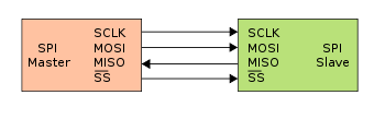
Typical connection between two SPI devices
Typical configuration
SPI is a four-wire interface, with the different lines being – MOSI [Master Out Slave In] -MISO [Master In Slave Out] -SCLK [Serial Clock OUT – generated by the master] -SS/CS [Slave Select or Chip Select, sometimes also labelled CE – Chip Enable]
SPI is a FULL DUPLEX interface, where the master initiates the communication frames between the various slave devices. This is usually done by pulling the particular device’s SS/CS pin low. Data is then shifted simultaneously into and out of the devices by means of the MOSI and MISO lines on the bus. The frequency of the serially shifted data is controlled by the SCLK line. This clock signal is generated by the master device.
It is important to note that MOST of the slave devices have a tri-state (HIGH IMPEDANCE) mode on their MISO pins. This electrically disconnects the MISO pin from the bus when the device is not selected via the SS/CS pin.
You should also note the SPI slave devices that do not have a tri-state mode on their MISO pins, should not be used on the same bus as devices that have without using an external tri-state buffer circuit between the non-tristate device and the rest of the devices on the MISO bus.
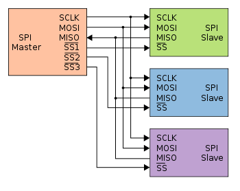
Typical connection between an SPI Master and three Slave devices
It is possible to connect multiple SPI slave devices to on Master device if you remember that each slave device will need its own dedicated SS/CS pin on the master. This can however quickly use a lot of IO pins on a microcontroller, thus being one of the disadvantages of SPI versus I2C. SPI is however quite a bit faster than I2C.
Data Transmission
To begin communication, the bus master configures the clock, using a frequency supported by the slave device, typically up to a few MHz. The master then selects the slave device with a logic level 0 on the select line. If a waiting period is required, such as for an analog-to-digital conversion, the master must wait for at least that period of time before issuing clock cycles.
During each SPI clock cycle, full-duplex data transmission occurs. The master sends a bit on the MOSI line and the slave reads it, while the slave sends a bit on the MISO line and the master reads it. This sequence is maintained even when only one-directional data transfer is intended.
A typical hardware setup using two shift registers to form an inter-chip circular buffer
Transmissions normally involve two shift registers of some given word-size, such as eight bits, one in the master and one in the slave; they are connected in a virtual ring topology. Data is usually shifted out with the most significant bit first. On the clock edge, both master and slave shift out a bit and output it on the transmission line to the counterpart. On the next clock edge, at each receiver the bit is sampled from the transmission line and set as a new least-significant bit of the shift register. After the register bits have been shifted out and in, the master and slave have exchanged register values. If more data needs to be exchanged, the shift registers are reloaded and the process repeats. Transmission may continue for any number of clock cycles. When complete, the master stops toggling the clock signal, and typically deselects the slave.
Transmissions often consist of eight-bit words. However, other word-sizes are also common, for example, sixteen-bit words for touch-screen controllers or audio codecs, such as the TSC2101 by Texas Instruments, or twelve-bit words for many digital-to-analogue or analogue-to-digital converters.
Every slave on the bus that has not been activated using its chip select line must disregard the input clock and MOSI signals and should not drive MISO (I.E. must have a tri-state output) although some devices need external tri-state buffers to implement this.
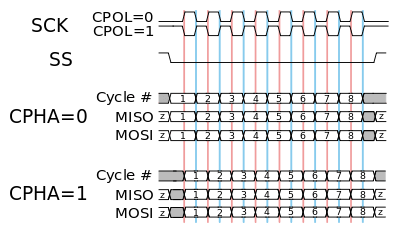
Clock polarity and phasing
In addition to setting the clock frequency, the master must also configure the clock polarity and phase with respect to the data. Motorola SPI Block Guide names these two options as CPOL and CPHA (for clock polarity and phase) respectively, a convention most vendors have also adopted.
The timing diagram is shown below. The timing is further described below and applies to both the master and the slave device.
CPOL determines the polarity of the clock. The polarities can be converted with a simple inverter.
CPOL=0 is a clock which idles at 0, and each cycle consists of a pulse of 1. That is, the leading edge is a rising edge, and the trailing edge is a falling edge.
CPOL=1 is a clock which idles at 1, and each cycle consists of a pulse of 0. That is, the leading edge is a falling edge, and the trailing edge is a rising edge.
CPHA determines the timing (i.e. phase) of the data bits relative to the clock pulses. Conversion between these two forms is non-trivial.
For CPHA=0, the “out” side changes the data on the trailing edge of the preceding clock cycle, while the “in” side captures the data on (or shortly after) the leading edge of the clock cycle. The out-side holds the data valid until the trailing edge of the current clock cycle. For the first cycle, the first bit must be on the MOSI line before the leading clock edge.
An alternative way of considering it is to say that a CPHA=0 cycle consists of a half cycle with the clock idle, followed by a half cycle with the clock asserted.
For CPHA=1, the “out” side changes the data on the leading edge of the current clock cycle, while the “in” side captures the data on (or shortly after) the trailing edge of the clock cycle. The out-side holds the data valid until the leading edge of the following clock cycle. For the last cycle, the slave holds the MISO line valid until slave select is de-selected.
An alternative way of considering it is to say that a CPHA=1 cycle consists of a half cycle with the clock asserted, followed by a half cycle with the clock idle.
A timing diagram showing clock polarity and phase. Red lines denote clock leading edges, and blue lines, trailing edges.
The MOSI and MISO signals are usually stable (at their reception points) for the half cycle until the next clock transition. SPI master and slave devices may well sample data at different points in that half cycle.
This adds more flexibility to the communication channel between the master and slave.
Mode numbers
The combinations of polarity and phases are often referred to as modes which are commonly numbered according to the following convention, with CPOL as the high order bit and CPHA as the low order bit:
For “Microchip PIC” / “ARM-based” microcontrollers (note that NCPHA is the inversion of CPHA):
SPI mode
Clock polarity (CPOL/CKP)
Clock phase (CPHA)
Clock edge (CKE/NCPHA)
0
0
0
1
1
0
1
0
2
1
0
1
3
1
1
0
For PIC32MX: SPI mode configure CKP, CKE and SMP bits. Set SMP bit and CKP, CKE two bits configured as above table.
Mode
CPOL
CPHA
0
0
0
1
0
1
2
1
0
3
1
1
For other microcontrollers:
Another commonly used notation represents the mode as a (CPOL, CPHA) tuple; e.g., the value ‘(0, 1)’ would indicate CPOL=0 and CPHA=1.
Note that in Full Duplex operation, the Master device could transmit and receive with different modes. For instance, it could transmit in Mode 0 and be receiving in Mode 1 at the same time.
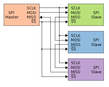
Independent Slave Configuration
In the independent slave configuration, there is an independent chip select line for each slave. This is the way SPI is normally used. The master asserts only one chip select at a time.
Pull-up resistors between the power source and chip select lines are recommended for systems where the master’s chip select pins may default to an undefined state. When separate software routines initialize each chip select and communicate with its slave, pull-up resistors prevent other uninitialized slaves from responding.
Since the MISO pins of the slaves are connected together, they are required to be tri-state pins (high, low or high-impedance), where the high-impedance output must be applied when the slave is not selected. Slave devices not supporting tri-state may be used in independent slave configuration by adding a tri-state buffer chip controlled by the chip select signal. (Since only a single signal line needs to be tri-stated per slave, one typical standard logic chip that contains four tristate buffers with independent gate inputs can be used to interface up to four slave devices to an SPI bus.)
Typical SPI configuration
Daisy chain configuration
Some products that implement SPI may be connected in a daisy chain configuration, the first slave output being connected to the second slave input, etc. The SPI port of each slave is designed to send out during the second group of clock pulses an exact copy of the data it received during the first group of clock pulses. The whole chain acts as a communication shift register; daisy chaining is often done with shift registers to provide a bank of inputs or outputs through SPI. Each slave copies input to output in the next clock cycle until the active low SS line goes high. Such a feature only requires a single SS line from the master, rather than a separate SS line for each slave.
Note that not all SPI devices support this. You should thus check your datasheet before using this configuration!
SPI Daisy Chain configuration
Valid Communications
Some slave devices are designed to ignore any SPI communications in which the number of clock pulses is greater than specified. Others do not care, ignoring extra inputs and continuing to shift the same output bit. It is common for different devices to use SPI communications with different lengths, as, for example, when SPI is used to access the scan chain of a digital IC by issuing a command word of one size (perhaps 32 bits) and then getting a response of a different size (perhaps 153 bits, one for each pin in that scan chain).
Interrupts
SPI devices sometimes use another signal line to send an interrupt signal to a host CPU. Examples include pen-down interrupts from touchscreen sensors, thermal limit alerts from temperature sensors, alarms issued by real-time clock chips, SDIO, and headset jack insertions from the sound codec in a cell phone. Interrupts are not covered by the SPI standard; their usage is neither forbidden nor specified by the standard. In other words, interrupts are outside the scope of the SPI standard and are optionally implemented independently from it.
Bit Banging a SPI Master – Example code
Below is an example of bit-banging the SPI protocol as an SPI master with CPOL=0, CPHA=0, and eight bits per transfer. The example is written in the C programming language. Because this is CPOL=0 the clock must be pulled low before the chip select is activated. The chip select line must be activated, which normally means being toggled low, for the peripheral before the start of the transfer, and then deactivated afterwards. Most peripherals allow or require several transfers while the select line is low; this routine might be called several times before deselecting the chip.
/*
 * Simultaneously transmit and receive a byte on the SPI.
 *
 * Polarity and phase are assumed to be both 0, i.e.:
 *   - input data is captured on rising edge of SCLK.
 *   - output data is propagated on falling edge of SCLK.
 *
 * Returns the received byte.
 */
uint8_t SPI_transfer_byte(uint8_t byte_out)
{
    uint8_t byte_in = 0;
    uint8_t bit;

    for (bit = 0x80; bit; bit >>= 1) {
        /* Shift-out a bit to the MOSI line */
        write_MOSI((byte_out & bit) ? HIGH : LOW);

        /* Delay for at least the peer's setup time */
        delay(SPI_SCLK_LOW_TIME);

        /* Pull the clock line high */
        write_SCLK(HIGH);

        /* Shift-in a bit from the MISO line */
        if (read_MISO() == HIGH)
            byte_in |= bit;

        /* Delay for at least the peer's hold time */
        delay(SPI_SCLK_HIGH_TIME);

        /* Pull the clock line low */
        write_SCLK(LOW);
    }

    return byte_in;
}
This concludes part 1 of my series on SPI. I hope you found it interesting and useful.
Today I will continue my series on I2C by showing you how to use multiple devices on the I2C bus. This will be an extremely short post, as it builds on skills that we have already covered.
All of these devices will be controlled from Arduino Uno, using the following libraries
LiquidCrystal_I2C.h to control the LCD screen, Wire.h and PCF8574.h to control the I2C IO extenders and Adafruit_GFX, Adafruit_SSD1306.h and SPI.h to control the SSD1306 128×32 OLED display.
With DuPont wires and breadboards being the reliable things they are, I decided that, after initial testing, I will not show you how to do button inputs on the PCF8574 at this stage. The amount of stray capacitance floating around on the breadboards, and small momentary push-button switches, made for a very impressive but unreliable mess of wires, with no real learning value to it 😉 Maybe some more on that later when I do a decent real-world example using these technologies 🙂
As the total distance between the devices is relatively short, it was not necessary to use pull-up resistors on the I2C bus in my setup. I suspect that that is due to the fact that they may already be included on some of my devices.
The circuit is quite straight forward.
Connect all SDA pins on the I2C devices together serially, and connect that to the Arduino SDA pin ( That is usually A4)
Connect all SCL pins on the I2C devices together serially, and connect that to the Arduino SCL pin ( That is usually A5)
A note: On my Uno clone, there is an additional I2C breakout at the top of the device, near the USB adapter. I chose to use that as well as A4 and A5, as the bus hung itself up when connected to the breadboard. Your mileage may vary on this one 🙂
Connect all 5v (Vcc) lines to 5v on the Arduino, and all Ground (GND) lines to GND on the Arduino.
Now connect 4 LEDs, through a suitable resistor ( 640 ohms up to 1k ohm ) to pin P0 and P1 on both of the PCF8574 IO extenders. Also, connect the other leg of the LED to ground.
I have powered my Uno from an external 5v power supply, as I did not want to pull too much current from the regulator on the actual Uno clone.
That should complete your hardware setup. Double check all your connections, and then load the i2c scanner sketch in the Arduino IDE, you may find it under the examples for the Wire.h library.
Power up the circuit, and upload the sketch to the Uno. Open the Serial Monitor.
You should see 4 I2C devices being detected. Note their addresses. If you dont see 4 devices, check your wiring and addresses. You may have a device with a conflicting address or a bad connection. If you used the breadboard to connect the bus, chances are very good that you will not see all the devices.
Good, if all of that is working, copy paste the following code into a new Arduino IDE window. I will explain the code in the section below:
/*
  Multiple devices on the I2C bus
  Maker and Iot Ideas, MakerIoT2020
*/
// Include the libraries that we will need
#include <SPI.h> // needed for OLED display.
#include <PCF8574.h> // PCF8574
#include <Wire.h> // Generic I2C library
#include <Adafruit_GFX.h> // for OLED display
#include <Adafruit_SSD1306.h> // for OLED display
#include <LiquidCrystal_I2C.h> // For I2C LCD display

// we need to define the size of the OLED screen

#define OLED_WIDTH 128
#define OLED_HEIGHT 32

// mine does not have an onboard reset pin. If yours do, specify the
// pin that it is connected to on the Arduino here. To use the
// Arduino reset pin, specify -1 as below

#define OLED_RESET -1

// Define the OLED display, width,hight protocol and reset pin
Adafruit_SSD1306 oled(OLED_WIDTH,OLED_HEIGHT, &Wire, OLED_RESET);

// Define the I2C LCD screen address and pin configuration
LiquidCrystal_I2C lcd(0x27,2,1,0,4,5,6,7,3,POSITIVE);

// Define the PCF8574 devices ( you can have up to 8 on a bus )
// but in this case, my LCD uses address 0x27, so I will have a
// conflicting address if I were to use 8 of them together with the
// LCD

PCF8574 Remote_1(0x20);
PCF8574 Remote_2(0x21);

// Note the I2C addresses. You can obtain them from the i2c_scanner

void setup() {
  // serial debugging if needed
  Serial.begin(115200);
  // Start OLED Display Init

  if (!oled.begin(SSD1306_SWITCHCAPVCC,0x3C)) { // Init the OLED
    Serial.println(F("OLED INIT FAILED"));
    for(;;); // Dont proceed ... loop forever
  }
  oled.display();
  delay(2000); // This delay is required to give display time to
  // initialise properly
  oled.clearDisplay();
  oled.setTextSize(0);
  oled.setTextColor(SSD1306_WHITE);
  oled.setCursor(0,0);
  oled.println("TEST SCREEN");
  oled.display();
  delay(2000);
  oled.clearDisplay();
  oled.setCursor(1,0);
  oled.println("OLED SCREEN ON");
  oled.display();

  // Start the LCD

  lcd.begin(16,2);

  // Set the initial state of the pins on the PCF8574 devices
  // I found that the PCF8574 library sometimes does funny things
  // This is also an example of how to use native i2c to set the
  // status of the pins

  Wire.begin();
  Wire.beginTransmission(0x20); // device 1
  Wire.write(0x00); // all ports off
  Wire.endTransmission();
  Wire.begin();
  Wire.beginTransmission(0x21); // device 2
  Wire.write(0x00); // all ports off
  Wire.endTransmission();
  // Set pinModes for PCF8574 devices
  // Note that there are two of them

  Remote_1.pinMode(P0,OUTPUT);
  Remote_1.pinMode(P1,OUTPUT);
  Remote_2.pinMode(P0,OUTPUT);
  Remote_2.pinMode(P1,OUTPUT);

  // Start both IO extenders

  Remote_1.begin();
  Remote_2.begin();

  // and set ports to low on both
  // you may find that if you ommit this step, they come up in an
  // unstable state.

  Remote_1.digitalWrite(P0,LOW);
  Remote_1.digitalWrite(P1,LOW);
  Remote_2.digitalWrite(P0,LOW);
  Remote_2.digitalWrite(P1,LOW);

}

void loop() {
  // Draw a character map on the OLED display.
  // This function is borrowed from the Adafruit library

  testdrawchar();

  // Write to the IO extenders

  Remote_1.digitalWrite(P0,HIGH);
  Remote_1.digitalWrite(P1,LOW);
  Remote_2.digitalWrite(P0,HIGH);
  Remote_2.digitalWrite(P1,LOW);

  // Display their status on the LCD
  lcd.setCursor(0,0);
  lcd.print(" R1 P0=1 P1=0");
  lcd.setCursor(0,1);
  lcd.print(" R2 P0=1 P1=0");
  delay(500);

  // Change status
  Remote_1.digitalWrite(P1,HIGH);
  Remote_1.digitalWrite(P0,LOW);
  Remote_2.digitalWrite(P1,HIGH);
  Remote_2.digitalWrite(P0,LOW);

  // Update LCD
  lcd.setCursor(0,0);
  lcd.print(" R1 P0=0 P1=1");
  lcd.setCursor(0,1);
  lcd.print(" R2 P0=0 P1=1");
  delay(500);
  // Do some graphics on the OLED display
  // Function borrowed from Adafruit
  testdrawrect();
  oled.clearDisplay();
  delay(500);
  // repeat indefinitely

}

void testdrawrect(void) {
  oled.clearDisplay();

  for(int16_t i=0; i<oled.height()/2; i+=2) {
    oled.drawRect(i, i, oled.width()-2*i, oled.height()-2*i, SSD1306_WHITE);
    oled.display(); // Update screen with each newly-drawn rectangle
    delay(1);
  }

  delay(500);
}

void testdrawchar(void) {
  oled.clearDisplay();

  oled.setTextSize(1);      // Normal 1:1 pixel scale
  oled.setTextColor(SSD1306_WHITE); // Draw white text
  oled.setCursor(0, 0);     // Start at top-left corner
  oled.cp437(true);         // Use full 256 char 'Code Page 437' font

  // Not all the characters will fit on the display. This is normal.
  // Library will draw what it can and the rest will be clipped.
  for(int16_t i=0; i<256; i++) {
    if(i == '\n') oled.write(' ');
    else          oled.write(i);
  }

  oled.display();
  delay(500);
}
This concludes a quick and dirty show and tell… I hope that it will stimulate questions and ideas for a lot of people.