What is SPI? Serial Peripheral Interface – Part 1

Introduction

The Serial Peripheral Interface is a synchronous serial communication interface for short-distance communication, it is typically used in embedded systems. The interface was developed by Motorola in the mid 1980’s and has become a very popular standard.

It is used with many kinds of sensors, LCD’s and also SD-Cards. SPI operates in a Master-Slave model, with a possibility of multiple slave devices, each selected in turn by a SS (slave select) or CS (chip select) pin that is usually pulled low by the master.

Typical connection between two SPI devices

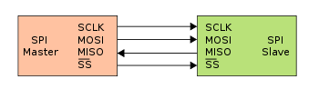
Typical configuration

SPI is a four-wire interface, with the different lines being
– MOSI [Master Out Slave In]
-MISO [Master In Slave Out]
-SCLK [Serial Clock OUT – generated by the master]
-SS/CS [Slave Select or Chip Select, sometimes also labelled CE – Chip Enable]

SPI is a FULL DUPLEX interface, where the master initiates the communication frames between the various slave devices. This is usually done by pulling the particular device’s SS/CS pin low. Data is then shifted simultaneously into and out of the devices by means of the MOSI and MISO lines on the bus. The frequency of the serially shifted data is controlled by the SCLK line. This clock signal is generated by the master device.

It is important to note that MOST of the slave devices have a tri-state (HIGH IMPEDANCE) mode on their MISO pins. This electrically disconnects the MISO pin from the bus when the device is not selected via the SS/CS pin.

You should also note the SPI slave devices that do not have a tri-state mode on their MISO pins, should not be used on the same bus as devices that have without using an external tri-state buffer circuit between the non-tristate device and the rest of the devices on the MISO bus.

Typical connection between an SPI Master and three Slave devices


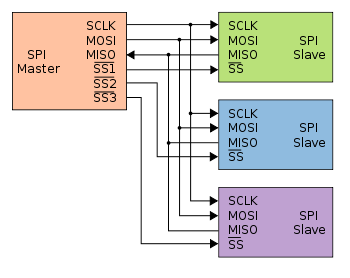
It is possible to connect multiple SPI slave devices to on Master device if you remember that each slave device will need its own dedicated SS/CS pin on the master. This can however quickly use a lot of IO pins on a microcontroller, thus being one of the disadvantages of SPI versus I2C. SPI is however quite a bit faster than I2C.

Data Transmission

To begin communication, the bus master configures the clock, using a frequency supported by the slave device, typically up to a few MHz. The master then selects the slave device with a logic level 0 on the select line. If a waiting period is required, such as for an analog-to-digital conversion, the master must wait for at least that period of time before issuing clock cycles.

During each SPI clock cycle, full-duplex data transmission occurs. The master sends a bit on the MOSI line and the slave reads it, while the slave sends a bit on the MISO line and the master reads it. This sequence is maintained even when only one-directional data transfer is intended.

A typical hardware setup using two shift registers to form an inter-chip circular buffer

Transmissions normally involve two shift registers of some given word-size, such as eight bits, one in the master and one in the slave; they are connected in a virtual ring topology. Data is usually shifted out with the most significant bit first. On the clock edge, both master and slave shift out a bit and output it on the transmission line to the counterpart. On the next clock edge, at each receiver the bit is sampled from the transmission line and set as a new least-significant bit of the shift register. After the register bits have been shifted out and in, the master and slave have exchanged register values. If more data needs to be exchanged, the shift registers are reloaded and the process repeats. Transmission may continue for any number of clock cycles. When complete, the master stops toggling the clock signal, and typically deselects the slave.

Transmissions often consist of eight-bit words. However, other word-sizes are also common, for example, sixteen-bit words for touch-screen controllers or audio codecs, such as the TSC2101 by Texas Instruments, or twelve-bit words for many digital-to-analogue or analogue-to-digital converters.

Every slave on the bus that has not been activated using its chip select line must disregard the input clock and MOSI signals and should not drive MISO (I.E. must have a tri-state output) although some devices need external tri-state buffers to implement this.

Clock polarity and phasing

In addition to setting the clock frequency, the master must also configure the clock polarity and phase with respect to the data. Motorola SPI Block Guide names these two options as CPOL and CPHA (for clock polarity and phase) respectively, a convention most vendors have also adopted.

The timing diagram is shown below. The timing is further described below and applies to both the master and the slave device.

  • CPOL determines the polarity of the clock. The polarities can be converted with a simple inverter.
  • CPOL=0 is a clock which idles at 0, and each cycle consists of a pulse of 1. That is, the leading edge is a rising edge, and the trailing edge is a falling edge.
  • CPOL=1 is a clock which idles at 1, and each cycle consists of a pulse of 0. That is, the leading edge is a falling edge, and the trailing edge is a rising edge.
  • CPHA determines the timing (i.e. phase) of the data bits relative to the clock pulses. Conversion between these two forms is non-trivial.
  • For CPHA=0, the “out” side changes the data on the trailing edge of the preceding clock cycle, while the “in” side captures the data on (or shortly after) the leading edge of the clock cycle. The out-side holds the data valid until the trailing edge of the current clock cycle. For the first cycle, the first bit must be on the MOSI line before the leading clock edge.
  • An alternative way of considering it is to say that a CPHA=0 cycle consists of a half cycle with the clock idle, followed by a half cycle with the clock asserted.
  • For CPHA=1, the “out” side changes the data on the leading edge of the current clock cycle, while the “in” side captures the data on (or shortly after) the trailing edge of the clock cycle. The out-side holds the data valid until the leading edge of the following clock cycle. For the last cycle, the slave holds the MISO line valid until slave select is de-selected.
  • An alternative way of considering it is to say that a CPHA=1 cycle consists of a half cycle with the clock asserted, followed by a half cycle with the clock idle.
A timing diagram showing clock polarity and phase. Red lines denote clock leading edges, and blue lines, trailing edges.

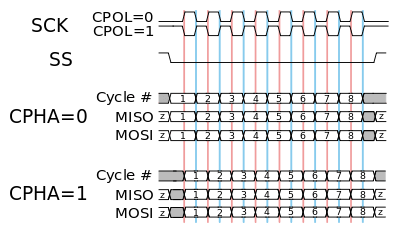
The MOSI and MISO signals are usually stable (at their reception points) for the half cycle until the next clock transition. SPI master and slave devices may well sample data at different points in that half cycle.

This adds more flexibility to the communication channel between the master and slave.

Mode numbers

The combinations of polarity and phases are often referred to as modes which are commonly numbered according to the following convention, with CPOL as the high order bit and CPHA as the low order bit:

For “Microchip PIC” / “ARM-based” microcontrollers (note that NCPHA is the inversion of CPHA):

SPI modeClock polarity
(CPOL/CKP)
Clock phase
(CPHA)
Clock edge
(CKE/NCPHA)
0001
1010
2101
3110
For PIC32MX: SPI mode configure CKP, CKE and SMP bits. Set SMP bit and CKP, CKE two bits configured as above table.
ModeCPOLCPHA
000
101
210
311
For other microcontrollers:

Another commonly used notation represents the mode as a (CPOL, CPHA) tuple; e.g., the value ‘(0, 1)’ would indicate CPOL=0 and CPHA=1.

Note that in Full Duplex operation, the Master device could transmit and receive with different modes. For instance, it could transmit in Mode 0 and be receiving in Mode 1 at the same time.

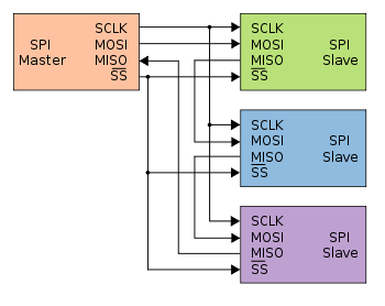
Independent Slave Configuration

In the independent slave configuration, there is an independent chip select line for each slave. This is the way SPI is normally used. The master asserts only one chip select at a time.

Pull-up resistors between the power source and chip select lines are recommended for systems where the master’s chip select pins may default to an undefined state. When separate software routines initialize each chip select and communicate with its slave, pull-up resistors prevent other uninitialized slaves from responding.

Since the MISO pins of the slaves are connected together, they are required to be tri-state pins (high, low or high-impedance), where the high-impedance output must be applied when the slave is not selected. Slave devices not supporting tri-state may be used in independent slave configuration by adding a tri-state buffer chip controlled by the chip select signal. (Since only a single signal line needs to be tri-stated per slave, one typical standard logic chip that contains four tristate buffers with independent gate inputs can be used to interface up to four slave devices to an SPI bus.)

Typical SPI configuration

Daisy chain configuration

Some products that implement SPI may be connected in a daisy chain configuration, the first slave output being connected to the second slave input, etc. The SPI port of each slave is designed to send out during the second group of clock pulses an exact copy of the data it received during the first group of clock pulses. The whole chain acts as a communication shift register; daisy chaining is often done with shift registers to provide a bank of inputs or outputs through SPI. Each slave copies input to output in the next clock cycle until the active low SS line goes high. Such a feature only requires a single SS line from the master, rather than a separate SS line for each slave.

Note that not all SPI devices support this. You should thus check your datasheet before using this configuration!

SPI Daisy Chain configuration

Valid Communications

Some slave devices are designed to ignore any SPI communications in which the number of clock pulses is greater than specified. Others do not care, ignoring extra inputs and continuing to shift the same output bit. It is common for different devices to use SPI communications with different lengths, as, for example, when SPI is used to access the scan chain of a digital IC by issuing a command word of one size (perhaps 32 bits) and then getting a response of a different size (perhaps 153 bits, one for each pin in that scan chain).

Interrupts

SPI devices sometimes use another signal line to send an interrupt signal to a host CPU. Examples include pen-down interrupts from touchscreen sensors, thermal limit alerts from temperature sensors, alarms issued by real-time clock chips, SDIO, and headset jack insertions from the sound codec in a cell phone. Interrupts are not covered by the SPI standard; their usage is neither forbidden nor specified by the standard. In other words, interrupts are outside the scope of the SPI standard and are optionally implemented independently from it.

Bit Banging a SPI Master – Example code

Below is an example of bit-banging the SPI protocol as an SPI master with CPOL=0, CPHA=0, and eight bits per transfer. The example is written in the C programming language. Because this is CPOL=0 the clock must be pulled low before the chip select is activated. The chip select line must be activated, which normally means being toggled low, for the peripheral before the start of the transfer, and then deactivated afterwards. Most peripherals allow or require several transfers while the select line is low; this routine might be called several times before deselecting the chip.

/*
 * Simultaneously transmit and receive a byte on the SPI.
 *
 * Polarity and phase are assumed to be both 0, i.e.:
 *   - input data is captured on rising edge of SCLK.
 *   - output data is propagated on falling edge of SCLK.
 *
 * Returns the received byte.
 */
uint8_t SPI_transfer_byte(uint8_t byte_out)
{
    uint8_t byte_in = 0;
    uint8_t bit;

    for (bit = 0x80; bit; bit >>= 1) {
        /* Shift-out a bit to the MOSI line */
        write_MOSI((byte_out & bit) ? HIGH : LOW);

        /* Delay for at least the peer's setup time */
        delay(SPI_SCLK_LOW_TIME);

        /* Pull the clock line high */
        write_SCLK(HIGH);

        /* Shift-in a bit from the MISO line */
        if (read_MISO() == HIGH)
            byte_in |= bit;

        /* Delay for at least the peer's hold time */
        delay(SPI_SCLK_HIGH_TIME);

        /* Pull the clock line low */
        write_SCLK(LOW);
    }

    return byte_in;
}

This concludes part 1 of my series on SPI. I hope you found it interesting and useful.

The OLED Display

Introduction

Adding a display to any project can instantly increase its visual appeal, as well as make the project easier to control. Displays available to Electronic enthusiasts mostly include some sort of LCD or even TFT display. LCD displays are usually bulky and very limited in their ability to display a lot of information, whereas TFT type displays are still a bit on the expensive side, and not very easy to interface with for the beginner.

Today, I would like to introduce a different type of display, which is available in an I2C as well as SPI version. These displays are very easily readable in almost any light conditions, lightweight, and most importantly, they are extremely cheap. I am talking about the OLED display of course… Many of us may already have one of them in our mobile phones, or even TV screen…

128×32 I2C OLED Display (40mmx10mm) [0.91″] Front view

Some Technical Data

An organic light-emitting diode (OLED or Organic LED), also known as an organic EL (organic electroluminescent) diode,[1][2] is a light-emitting diode (LED) in which the emissive electroluminescent layer is a film of organic compound that emits light in response to an electric current. This organic layer is situated between two electrodes; typically, at least one of these electrodes is transparent. OLEDs are used to create digital displays in devices such as television screens, computer monitors, portable systems such as smartphoneshandheld game consoles and PDAs. A major area of research is the development of white OLED devices for use in solid-state lighting applications.[3][4][5]

There are two main families of OLED: those based on small molecules and those employing polymers. Adding mobile ions to an OLED creates a light-emitting electrochemical cell (LEC) which has a slightly different mode of operation. An OLED display can be driven with a passive-matrix (PMOLED) or active-matrix (AMOLED) control scheme. In the PMOLED scheme, each row (and line) in the display is controlled sequentially, one by one,[6] whereas AMOLED control uses a thin-film transistor backplane to directly access and switch each individual pixel on or off, allowing for higher resolution and larger display sizes.

An OLED display works without a backlight because it emits visible light. Thus, it can display deep black levels and can be thinner and lighter than a liquid crystal display (LCD). In low ambient light conditions (such as a dark room), an OLED screen can achieve a higher contrast ratio than an LCD, regardless of whether the LCD uses cold cathode fluorescent lamps or an LED backlight. OLED displays are made in the same way as LCDs, but after TFT (for active matrix displays), addressable grid (for passive matrix displays) or ITO segment (for segment displays) formation, the display is coated with hole injection, transport and blocking layers, as well with electroluminescent material after the 2 first layers, after which ITO or metal may be applied again as a cathode and later the entire stack of materials is encapsulated. The TFT layer, addressable grid or ITO segments serve as or are connected to the anode, which may be made of ITO or metal.[7][8] OLEDs can be made flexible and transparent, with transparent displays being used in smartphones with optical fingerprint scanners and flexible displays being used in foldable smartphones.

The full article is available here if you are interested.

128×32 I2C OLED Display (40mmx10mm) [0.91″] Back view

Connecting the circuit

This display is once again extremely easy to connect, as it uses the very versatile I2C protocol. (An SPI version is also available).

Connecting 128×32 OLED display to an Arduino Uno Clone

Connect the following wires to the Arduino / ESP32
+5v (red) to the VCC pin on the display
Gnd to Gnd
SDA (A4 on Uno) to SDA, and SCL (A5 on Uno) to SCL

The Software Libraries

The 128×32 OLED display that we will be using today, is based on the SSD1306. We will thus be using a library suplied by Adafruit to interface with this chip. There are various other libraries available, but I have found the Adafruit library the most stable.

To load this, start by opening the Arduino IDE, and go to the Sketch->Include Library->Manage Libraries option on the menu

The Library Manager will now open

We need to install two (2) Libraries

– Adafruit GFX ( this is for graphics)
– Adafruit SSD1306 ( to control the actual display )

Click on “Close” after installation is completed.

Using the display

We will use one of the standard Adafruit examples to show you the capabilities of the tiny little screen. The example are so straight forward to use, that I find it unnecessary to say anything else about it 🙂

Open the ssd1306_128x32_ic2 Example from the Examples menu in the Arduino IDE and upload it to your Arduino, making sure that you set the dimensions of your screen first (in my case 128×32 )

/**************************************************************************
 This is an example for our Monochrome OLEDs based on SSD1306 drivers

 Pick one up today in the adafruit shop!
 ------> http://www.adafruit.com/category/63_98

 This example is for a 128x32 pixel display using I2C to communicate
 3 pins are required to interface (two I2C and one reset).

 Adafruit invests time and resources providing this open
 source code, please support Adafruit and open-source
 hardware by purchasing products from Adafruit!

 Written by Limor Fried/Ladyada for Adafruit Industries,
 with contributions from the open source community.
 BSD license, check license.txt for more information
 All text above, and the splash screen below must be
 included in any redistribution.
 **************************************************************************/

#include <SPI.h>
#include <Wire.h>
#include <Adafruit_GFX.h>
#include <Adafruit_SSD1306.h>

#define SCREEN_WIDTH 128 // OLED display width, in pixels
#define SCREEN_HEIGHT 32 // OLED display height, in pixels

// Declaration for an SSD1306 display connected to I2C (SDA, SCL pins)
#define OLED_RESET     4 // Reset pin # (or -1 if sharing Arduino reset pin)
Adafruit_SSD1306 display(SCREEN_WIDTH, SCREEN_HEIGHT, &Wire, OLED_RESET);

#define NUMFLAKES     10 // Number of snowflakes in the animation example

#define LOGO_HEIGHT   16
#define LOGO_WIDTH    16
static const unsigned char PROGMEM logo_bmp[] =
{ B00000000, B11000000,
  B00000001, B11000000,
  B00000001, B11000000,
  B00000011, B11100000,
  B11110011, B11100000,
  B11111110, B11111000,
  B01111110, B11111111,
  B00110011, B10011111,
  B00011111, B11111100,
  B00001101, B01110000,
  B00011011, B10100000,
  B00111111, B11100000,
  B00111111, B11110000,
  B01111100, B11110000,
  B01110000, B01110000,
  B00000000, B00110000 };

void setup() {
  Serial.begin(9600);

  // SSD1306_SWITCHCAPVCC = generate display voltage from 3.3V internally
  if(!display.begin(SSD1306_SWITCHCAPVCC, 0x3C)) { // Address 0x3C for 128x32
    Serial.println(F("SSD1306 allocation failed"));
    for(;;); // Don't proceed, loop forever
  }

  // Show initial display buffer contents on the screen --
  // the library initializes this with an Adafruit splash screen.
  display.display();
  delay(2000); // Pause for 2 seconds

  // Clear the buffer
  display.clearDisplay();

  // Draw a single pixel in white
  display.drawPixel(10, 10, SSD1306_WHITE);

  // Show the display buffer on the screen. You MUST call display() after
  // drawing commands to make them visible on screen!
  display.display();
  delay(2000);
  // display.display() is NOT necessary after every single drawing command,
  // unless that's what you want...rather, you can batch up a bunch of
  // drawing operations and then update the screen all at once by calling
  // display.display(). These examples demonstrate both approaches...

  testdrawline();      // Draw many lines

  testdrawrect();      // Draw rectangles (outlines)

  testfillrect();      // Draw rectangles (filled)

  testdrawcircle();    // Draw circles (outlines)

  testfillcircle();    // Draw circles (filled)

  testdrawroundrect(); // Draw rounded rectangles (outlines)

  testfillroundrect(); // Draw rounded rectangles (filled)

  testdrawtriangle();  // Draw triangles (outlines)

  testfilltriangle();  // Draw triangles (filled)

  testdrawchar();      // Draw characters of the default font

  testdrawstyles();    // Draw 'stylized' characters

  testscrolltext();    // Draw scrolling text

  testdrawbitmap();    // Draw a small bitmap image

  // Invert and restore display, pausing in-between
  display.invertDisplay(true);
  delay(1000);
  display.invertDisplay(false);
  delay(1000);

  testanimate(logo_bmp, LOGO_WIDTH, LOGO_HEIGHT); // Animate bitmaps
}

void loop() {
}

void testdrawline() {
  int16_t i;

  display.clearDisplay(); // Clear display buffer

  for(i=0; i<display.width(); i+=4) {
    display.drawLine(0, 0, i, display.height()-1, SSD1306_WHITE);
    display.display(); // Update screen with each newly-drawn line
    delay(1);
  }
  for(i=0; i<display.height(); i+=4) {
    display.drawLine(0, 0, display.width()-1, i, SSD1306_WHITE);
    display.display();
    delay(1);
  }
  delay(250);

  display.clearDisplay();

  for(i=0; i<display.width(); i+=4) {
    display.drawLine(0, display.height()-1, i, 0, SSD1306_WHITE);
    display.display();
    delay(1);
  }
  for(i=display.height()-1; i>=0; i-=4) {
    display.drawLine(0, display.height()-1, display.width()-1, i, SSD1306_WHITE);
    display.display();
    delay(1);
  }
  delay(250);

  display.clearDisplay();

  for(i=display.width()-1; i>=0; i-=4) {
    display.drawLine(display.width()-1, display.height()-1, i, 0, SSD1306_WHITE);
    display.display();
    delay(1);
  }
  for(i=display.height()-1; i>=0; i-=4) {
    display.drawLine(display.width()-1, display.height()-1, 0, i, SSD1306_WHITE);
    display.display();
    delay(1);
  }
  delay(250);

  display.clearDisplay();

  for(i=0; i<display.height(); i+=4) {
    display.drawLine(display.width()-1, 0, 0, i, SSD1306_WHITE);
    display.display();
    delay(1);
  }
  for(i=0; i<display.width(); i+=4) {
    display.drawLine(display.width()-1, 0, i, display.height()-1, SSD1306_WHITE);
    display.display();
    delay(1);
  }

  delay(2000); // Pause for 2 seconds
}

void testdrawrect(void) {
  display.clearDisplay();

  for(int16_t i=0; i<display.height()/2; i+=2) {
    display.drawRect(i, i, display.width()-2*i, display.height()-2*i, SSD1306_WHITE);
    display.display(); // Update screen with each newly-drawn rectangle
    delay(1);
  }

  delay(2000);
}

void testfillrect(void) {
  display.clearDisplay();

  for(int16_t i=0; i<display.height()/2; i+=3) {
    // The INVERSE color is used so rectangles alternate white/black
    display.fillRect(i, i, display.width()-i*2, display.height()-i*2, SSD1306_INVERSE);
    display.display(); // Update screen with each newly-drawn rectangle
    delay(1);
  }

  delay(2000);
}

void testdrawcircle(void) {
  display.clearDisplay();

  for(int16_t i=0; i<max(display.width(),display.height())/2; i+=2) {
    display.drawCircle(display.width()/2, display.height()/2, i, SSD1306_WHITE);
    display.display();
    delay(1);
  }

  delay(2000);
}

void testfillcircle(void) {
  display.clearDisplay();

  for(int16_t i=max(display.width(),display.height())/2; i>0; i-=3) {
    // The INVERSE color is used so circles alternate white/black
    display.fillCircle(display.width() / 2, display.height() / 2, i, SSD1306_INVERSE);
    display.display(); // Update screen with each newly-drawn circle
    delay(1);
  }

  delay(2000);
}

void testdrawroundrect(void) {
  display.clearDisplay();

  for(int16_t i=0; i<display.height()/2-2; i+=2) {
    display.drawRoundRect(i, i, display.width()-2*i, display.height()-2*i,
      display.height()/4, SSD1306_WHITE);
    display.display();
    delay(1);
  }

  delay(2000);
}

void testfillroundrect(void) {
  display.clearDisplay();

  for(int16_t i=0; i<display.height()/2-2; i+=2) {
    // The INVERSE color is used so round-rects alternate white/black
    display.fillRoundRect(i, i, display.width()-2*i, display.height()-2*i,
      display.height()/4, SSD1306_INVERSE);
    display.display();
    delay(1);
  }

  delay(2000);
}

void testdrawtriangle(void) {
  display.clearDisplay();

  for(int16_t i=0; i<max(display.width(),display.height())/2; i+=5) {
    display.drawTriangle(
      display.width()/2  , display.height()/2-i,
      display.width()/2-i, display.height()/2+i,
      display.width()/2+i, display.height()/2+i, SSD1306_WHITE);
    display.display();
    delay(1);
  }

  delay(2000);
}

void testfilltriangle(void) {
  display.clearDisplay();

  for(int16_t i=max(display.width(),display.height())/2; i>0; i-=5) {
    // The INVERSE color is used so triangles alternate white/black
    display.fillTriangle(
      display.width()/2  , display.height()/2-i,
      display.width()/2-i, display.height()/2+i,
      display.width()/2+i, display.height()/2+i, SSD1306_INVERSE);
    display.display();
    delay(1);
  }

  delay(2000);
}

void testdrawchar(void) {
  display.clearDisplay();

  display.setTextSize(1);      // Normal 1:1 pixel scale
  display.setTextColor(SSD1306_WHITE); // Draw white text
  display.setCursor(0, 0);     // Start at top-left corner
  display.cp437(true);         // Use full 256 char 'Code Page 437' font

  // Not all the characters will fit on the display. This is normal.
  // Library will draw what it can and the rest will be clipped.
  for(int16_t i=0; i<256; i++) {
    if(i == '\n') display.write(' ');
    else          display.write(i);
  }

  display.display();
  delay(2000);
}

void testdrawstyles(void) {
  display.clearDisplay();

  display.setTextSize(1);             // Normal 1:1 pixel scale
  display.setTextColor(SSD1306_WHITE);        // Draw white text
  display.setCursor(0,0);             // Start at top-left corner
  display.println(F("Hello, world!"));

  display.setTextColor(SSD1306_BLACK, SSD1306_WHITE); // Draw 'inverse' text
  display.println(3.141592);

  display.setTextSize(2);             // Draw 2X-scale text
  display.setTextColor(SSD1306_WHITE);
  display.print(F("0x")); display.println(0xDEADBEEF, HEX);

  display.display();
  delay(2000);
}

void testscrolltext(void) {
  display.clearDisplay();

  display.setTextSize(2); // Draw 2X-scale text
  display.setTextColor(SSD1306_WHITE);
  display.setCursor(10, 0);
  display.println(F("scroll"));
  display.display();      // Show initial text
  delay(100);

  // Scroll in various directions, pausing in-between:
  display.startscrollright(0x00, 0x0F);
  delay(2000);
  display.stopscroll();
  delay(1000);
  display.startscrollleft(0x00, 0x0F);
  delay(2000);
  display.stopscroll();
  delay(1000);
  display.startscrolldiagright(0x00, 0x07);
  delay(2000);
  display.startscrolldiagleft(0x00, 0x07);
  delay(2000);
  display.stopscroll();
  delay(1000);
}

void testdrawbitmap(void) {
  display.clearDisplay();

  display.drawBitmap(
    (display.width()  - LOGO_WIDTH ) / 2,
    (display.height() - LOGO_HEIGHT) / 2,
    logo_bmp, LOGO_WIDTH, LOGO_HEIGHT, 1);
  display.display();
  delay(1000);
}

#define XPOS   0 // Indexes into the 'icons' array in function below
#define YPOS   1
#define DELTAY 2

void testanimate(const uint8_t *bitmap, uint8_t w, uint8_t h) {
  int8_t f, icons[NUMFLAKES][3];

  // Initialize 'snowflake' positions
  for(f=0; f< NUMFLAKES; f++) {
    icons[f][XPOS]   = random(1 - LOGO_WIDTH, display.width());
    icons[f][YPOS]   = -LOGO_HEIGHT;
    icons[f][DELTAY] = random(1, 6);
    Serial.print(F("x: "));
    Serial.print(icons[f][XPOS], DEC);
    Serial.print(F(" y: "));
    Serial.print(icons[f][YPOS], DEC);
    Serial.print(F(" dy: "));
    Serial.println(icons[f][DELTAY], DEC);
  }

  for(;;) { // Loop forever...
    display.clearDisplay(); // Clear the display buffer

    // Draw each snowflake:
    for(f=0; f< NUMFLAKES; f++) {
      display.drawBitmap(icons[f][XPOS], icons[f][YPOS], bitmap, w, h, SSD1306_WHITE);
    }

    display.display(); // Show the display buffer on the screen
    delay(200);        // Pause for 1/10 second

    // Then update coordinates of each flake...
    for(f=0; f< NUMFLAKES; f++) {
      icons[f][YPOS] += icons[f][DELTAY];
      // If snowflake is off the bottom of the screen...
      if (icons[f][YPOS] >= display.height()) {
        // Reinitialize to a random position, just off the top
        icons[f][XPOS]   = random(1 - LOGO_WIDTH, display.width());
        icons[f][YPOS]   = -LOGO_HEIGHT;
        icons[f][DELTAY] = random(1, 6);
      }
    }
  }
}

I hope that you find this useful and inspiring.
Thank you