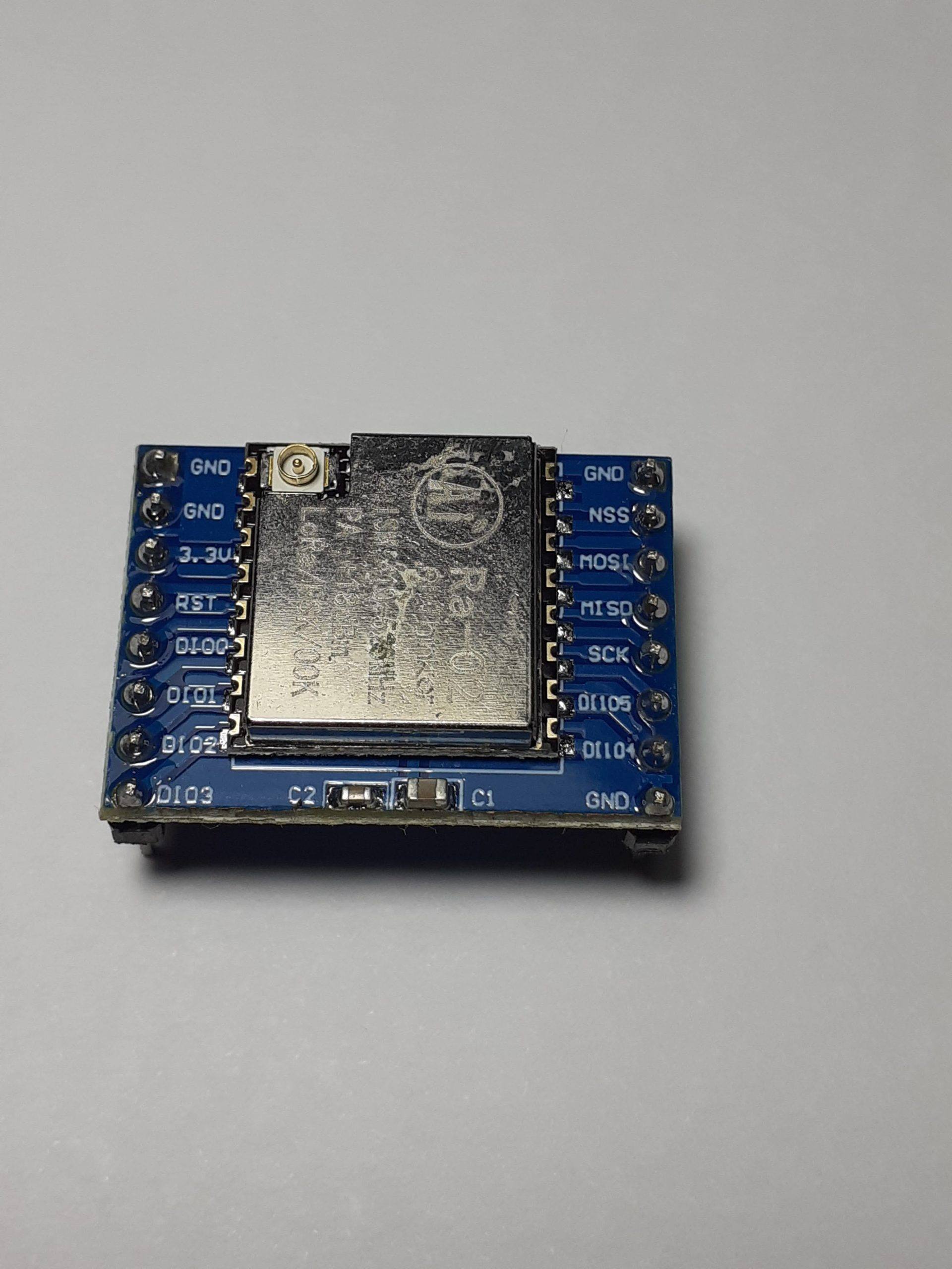
Most Makers and electronics enthusiasts may already know of the RA-02 LoRa Module. Many of them might own an RA-02 Breakout module or two… For those who do, they will surely know about the problems encountered with using this particular breakout module…
The RA-02 module, in itself, is a great piece of kit, and when used on a custom PCB, which was designed with all the little secrets of this module taken into consideration, is a pleasure. Using the RA-02 breakout module, in its existing form factor, does however present quite a few unique challenges, which, if you are unaware of them, can cause quite a few frustrating moments, or even result in permanent damage to the module…
In this post, we will focus on :
1) The Challenges of the existing commercially available RA-02 Breakout Module
2) My Solution to above mentioned Challenges
3)Testing the Module
– Maker Uno – An Arduino Uno Clone
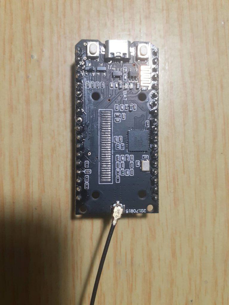
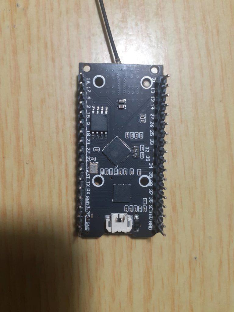
– Maker Nano RP2040
– Maker Pi Pico – Raspberry Pi Pico breakout module
What are these challenges:
1) The module is based on the SX1278 chip from Semtech and is a 3v device. The IO pins are NOT 5v compatible but seem to work for a few hours or so when used with 5v… This causes many people, especially on Youtube, to assume that it is ok to send 5v logic signals to this module…
I have still not seen any Youtube video telling viewers to at least use a resister divider or logic converter… People just don’t know, and those that know seem to be keeping quiet!
Adding logic converters is in fact specified by the datasheet.
2) Adding logic converters means adding additional wiring, and for a breadboard based project, that adds to the complexity.
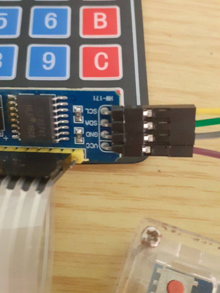
3) You have a total of 4 ground pins that need to be connected. not connecting all of them, causes funny things to happen, from overheating down to failure… ( My personal experience while researching this project)
4) The existing breakout module is not breadboarding compatible, resulting in a floating assembly with wires going everywhere, which results in unstable connections etc…
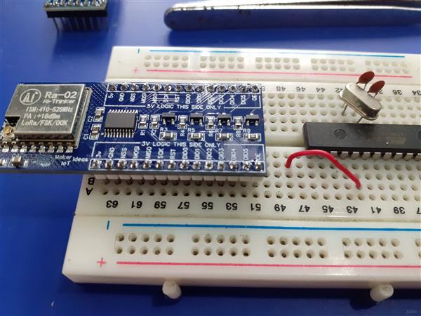
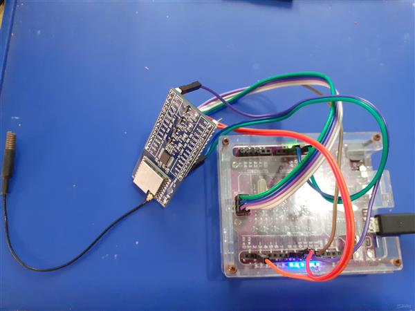
Basically something similar to the picture below:
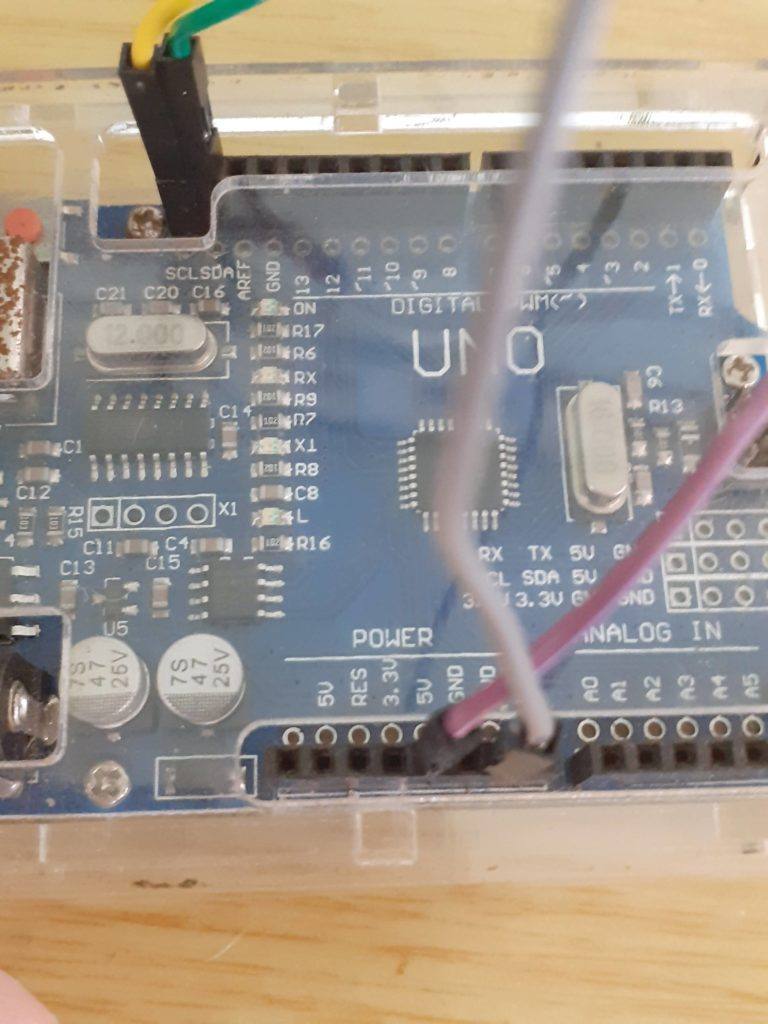
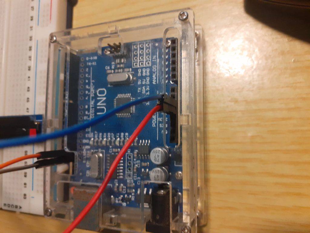
In this picture, I have an existing RA-02 Breakout Module, with an 8 channel Logic converter and an Arduino Uno clone, along with all the needed wiring to make this setup possible… Quite a lot of wires indeed…
My solution:
I design and use quite a few LoRa PCBs and on all of them, I implement logic conversion using the BSS138 N-MOS Mosfet and 10k resistors. It is a cheap and reliable solution, but it can take up quite a lot of space on a PCB, as this means 11 Mosfets and 22 10k resistors if I were to provide level conversion to all of the RA-02’s GPIO and IO pins…
I also have the constant problem of many unnecessary wires, many of which sometimes fail straight out of the box, when prototyping something. I partly solved that by designing a few dedicated PCB solutions, but that is not always ideal,
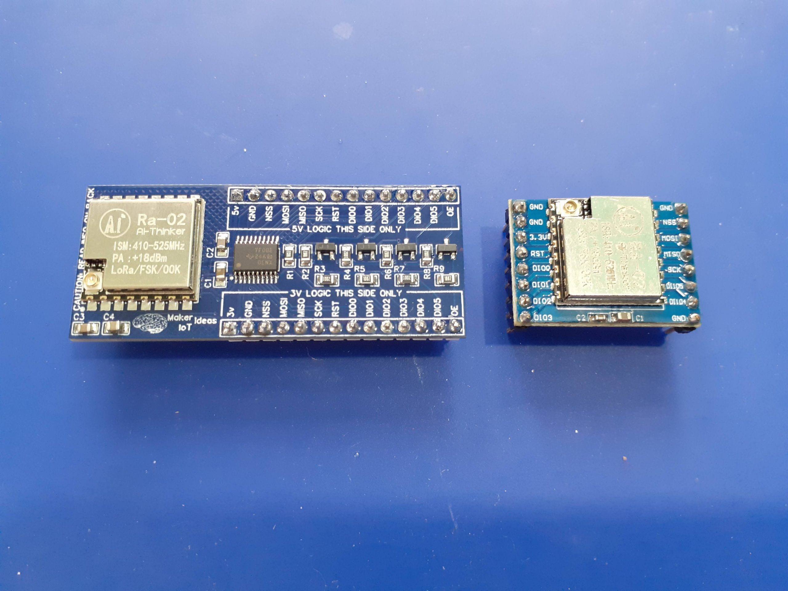
Using a dedicated Logic Converter IC, and Mosfet based converters to make up the difference, on a breadboard compatible module, seemed like a good idea, so I went ahead and designed the following solution:
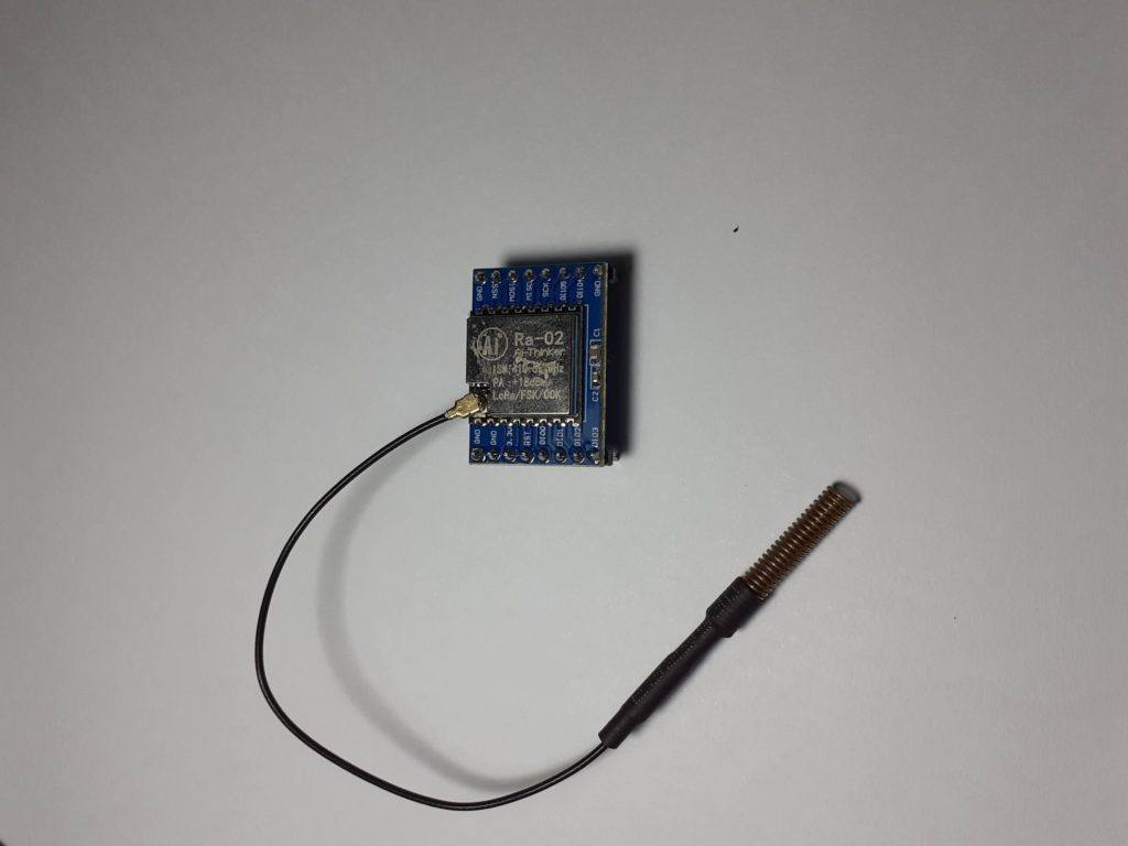
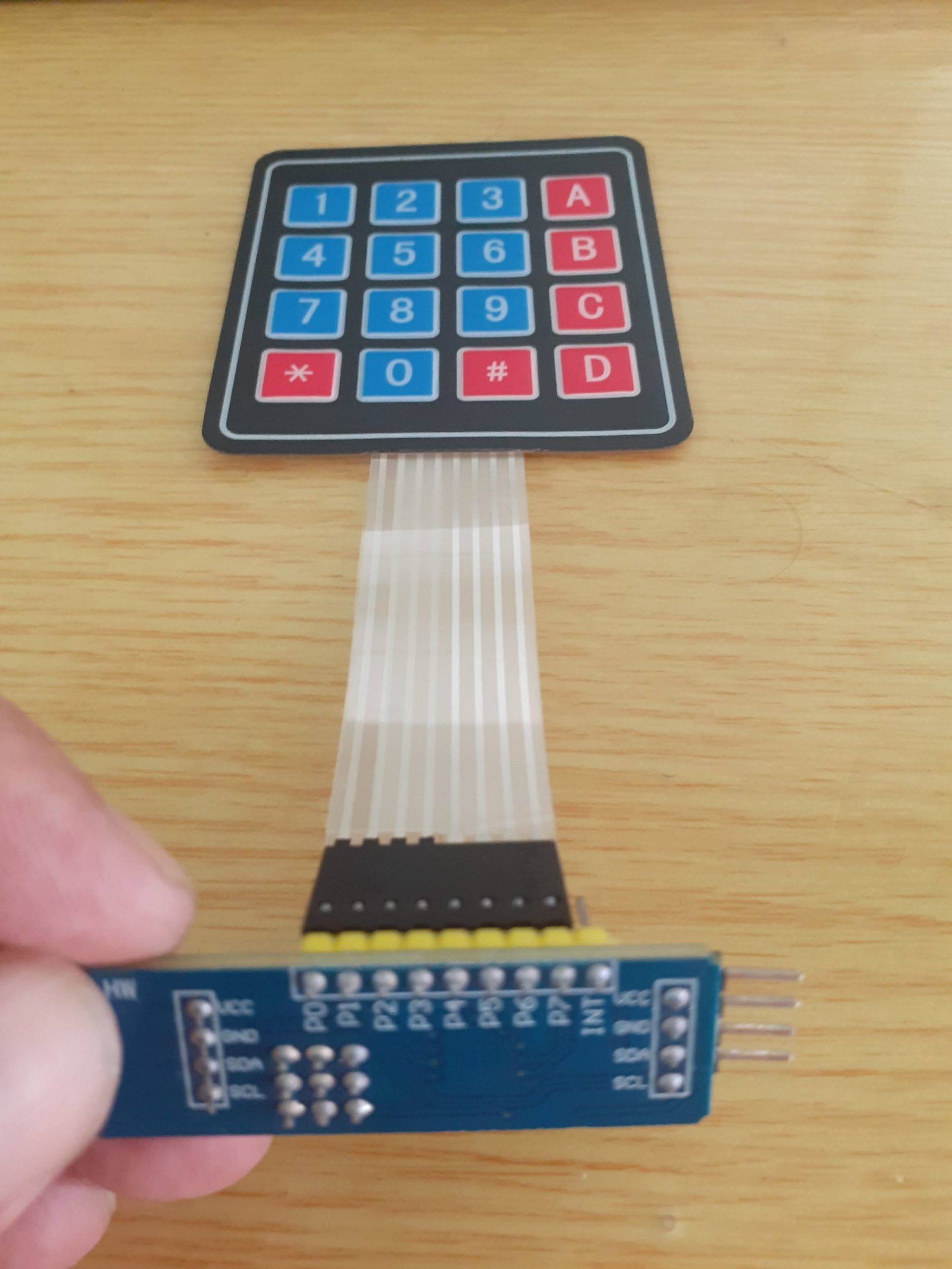
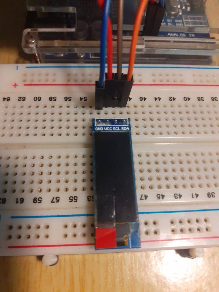
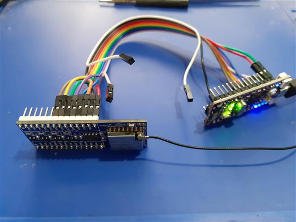
The breakout board module is breadboard compatible, and also has clearly marked pins to indicate the 3v and 5v sides of the module.
Testing the Module:
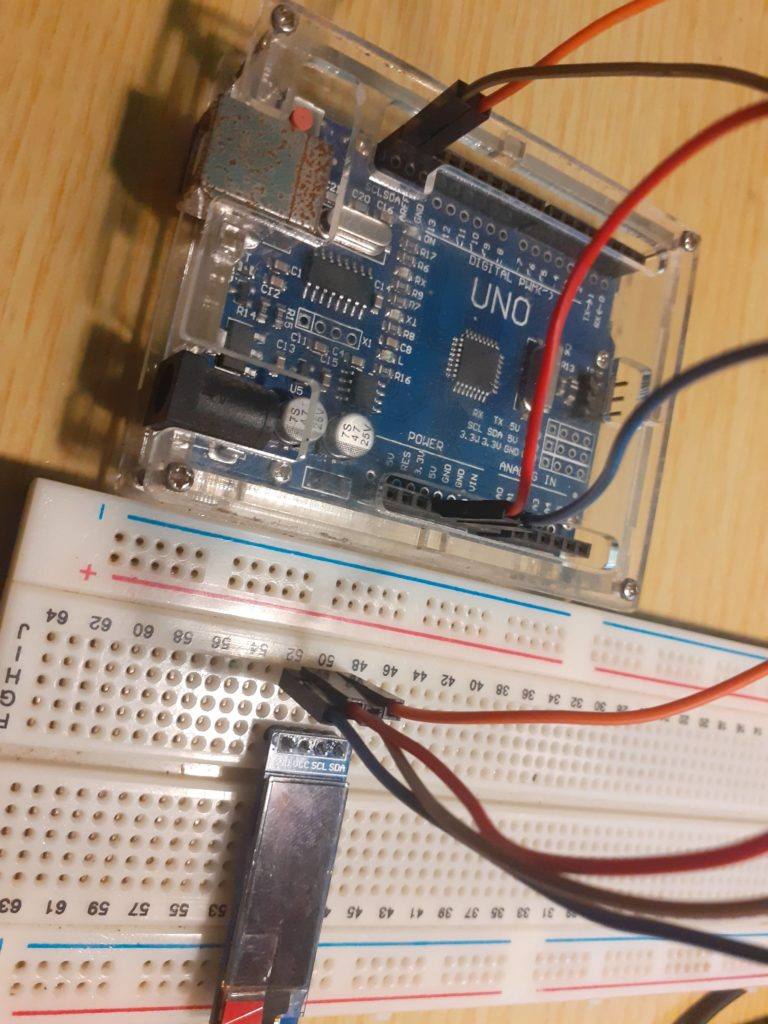
Using a 5v device ( Cytron’s Maker Uno )
For my first test, I decided to test with an Arduino Uno Clone, since that is what most Makers and students will have access to. I used Cytron’s Maker Uno platform, which is equipped with some added goodies, in the form of diagnostic LED etc to make prototyping a lot easier.
As we can clearly see, It is only necessary to connect to the 5v logic side of the module, as well as provide 3v and 5v + GND to the module
In this test, I used Sandeep Mistry’s LoRa Library, with the Arduino IDE to do a quick test sketch.
Connections are as follows:
RA-02 Module Maker Uno
MISO D12
MOSI D11
SCK D13
NSS D10
RST D9
DIO0 D2
OE D8
Let us look at some important sections though, to thoroughly understand how to use the module:
Pin Declaration
#include <SPI.h> // include libraries
#include <LoRa.h> // I used Sandeep Mistry’s LoRa Library, as it is easy to use and understand
const int csPin = 10; // LoRa radio chip select
const int resetPin = 9; // LoRa radio reset
const int irqPin = 2; // change for your board; must be a hardware interrupt pin
const int OEPin = 8; // Output Enable Pin, to enable the Logic Converter
In the Setup function, we need to do a bit of extra work, since our Maker Uno ( or your Arduino Uno ) is a 5v device…
void setup() {
Serial.begin(115200); // initialize serial
pinMode(OEPin,OUTPUT); // Setup the OE pin as an Outout
digitalWrite(OEPin,HIGH); // and Pull it High to enable the logic converter
while (!Serial);
Serial.println(“LoRa Duplex – Set spreading factor”);
// override the default CS, reset, and IRQ pins (optional)
LoRa.setPins(csPin, resetPin, irqPin); // set CS, reset, IRQ pin
if (!LoRa.begin(433E6)) { // initialize ratio at 433 MHz
Serial.println(“LoRa init failed. Check your connections.”);
while (true); // if failed, do nothing
}
LoRa.setSpreadingFactor(8); // ranges from 6-12,default 7 see API docs
Serial.println(“LoRa init succeeded.”);
}
A comparison, using the standard RS-02 Breakout module, together with one of my own “Arduino type PCB”
ATMEGA328P with 8 Channel Logic Converter.
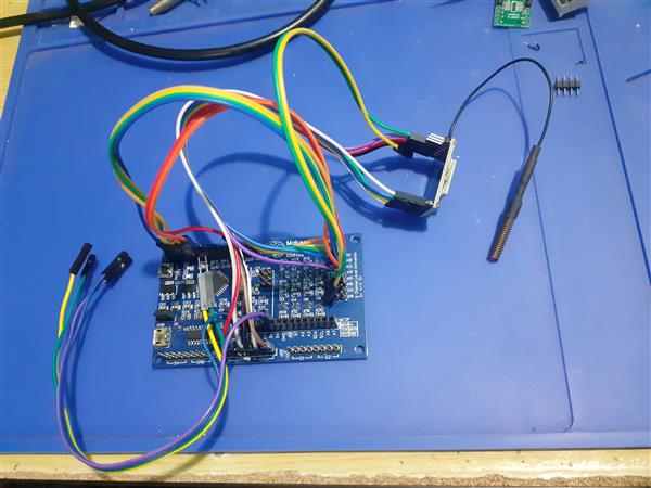
As we can see, you need quite a lot more wires to make this work. It is also worth noting that we have only 8 level converters on this ATMEGA328P PCB, in order to use all of the RA-02’s GPIO, we will need to add an additional external logic converter as well.
Using a 3v Device:
For my second test, I decided to be a bit brave, and try to use the new Raspberry Pi Pico ( RP2040 Microprocessor ). I have quite a few of them lying around and have never really done a lot with them, due to the fact that I do not really like using MicroPython or CircuitPython, and also because the recently released Arduino Core for the RP2040 still being quite new… I decided to use a development board that I recently bought from Cytron, the Maker Nano RP2040, as it has all the added diagnostic features to make my life a bit easier, I will also include a test with an original Pi Pico board, to make it more accessible to everyone out there.
Once again, I used Sandeep Mistry’s LoRa Library, with the exact same Arduino sketch, used for the Maker Uno test. (I obviously needed to change the pin numbers though, as the RP2040 uses different pins for its SPI interface).
Maker Nano RP2040 RA-02 Breakout Module
NSS 17
MOSI 19
MISO 16
SCK 18
RST 9
DIO0 8
In this case, we DO NOT need the OE pin, as the RP2040 is a native 3v device. The level converter can thus stay disabled, with its pins in tri-state ( high impedance ) mode.
If we look at the code, it is similar to the Maker Uno’s code, with only the Pin declarations needing a change
#include <SPI.h> // include libraries
#include <LoRa.h>
const int csPin = 17; // LoRa radio chip select
const int resetPin = 9; // LoRa radio reset
const int irqPin = 8; // change for your board; must be a hardware interrupt pin
byte msgCount = 0; // count of outgoing messages
int interval = 2000; // interval between sends
long lastSendTime = 0; // time of last packet send
// Note that SPI has different names on the RP2040, and it has 2 SPI ports. We used port 0
// CIPO (Miso) is on pin 16
// COPI (Mosi) is on pin 19
// SCK is on pin 18
// CE/SS is on pin 17, as already declared above
I did not use a breadboard, in order to make things as easy as possible.
Cytron’s Maker Pi Pico – A Pi Pico on a breakout PCB
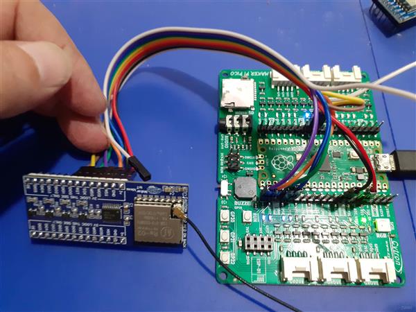
To make things a bit easier, without having to resort to using a breadboard, I decided to do the Original Pi Pico test using the Maker Pi Pico PCB. This PCB is basically a big breakout module, with detailed pin numbers and some diagnostic LEDs, but it also uses a native Pi Pico, soldered directly to the PCB, by means of the castellated holes… So, While technically not being a true standalone Pico, It makes my life easier and was thus used for the test, as I can be sure that the pins are labelled exactly the same as on the original Pico.
The code used for the Maker Nano RP2040 works perfectly, with no changes required.
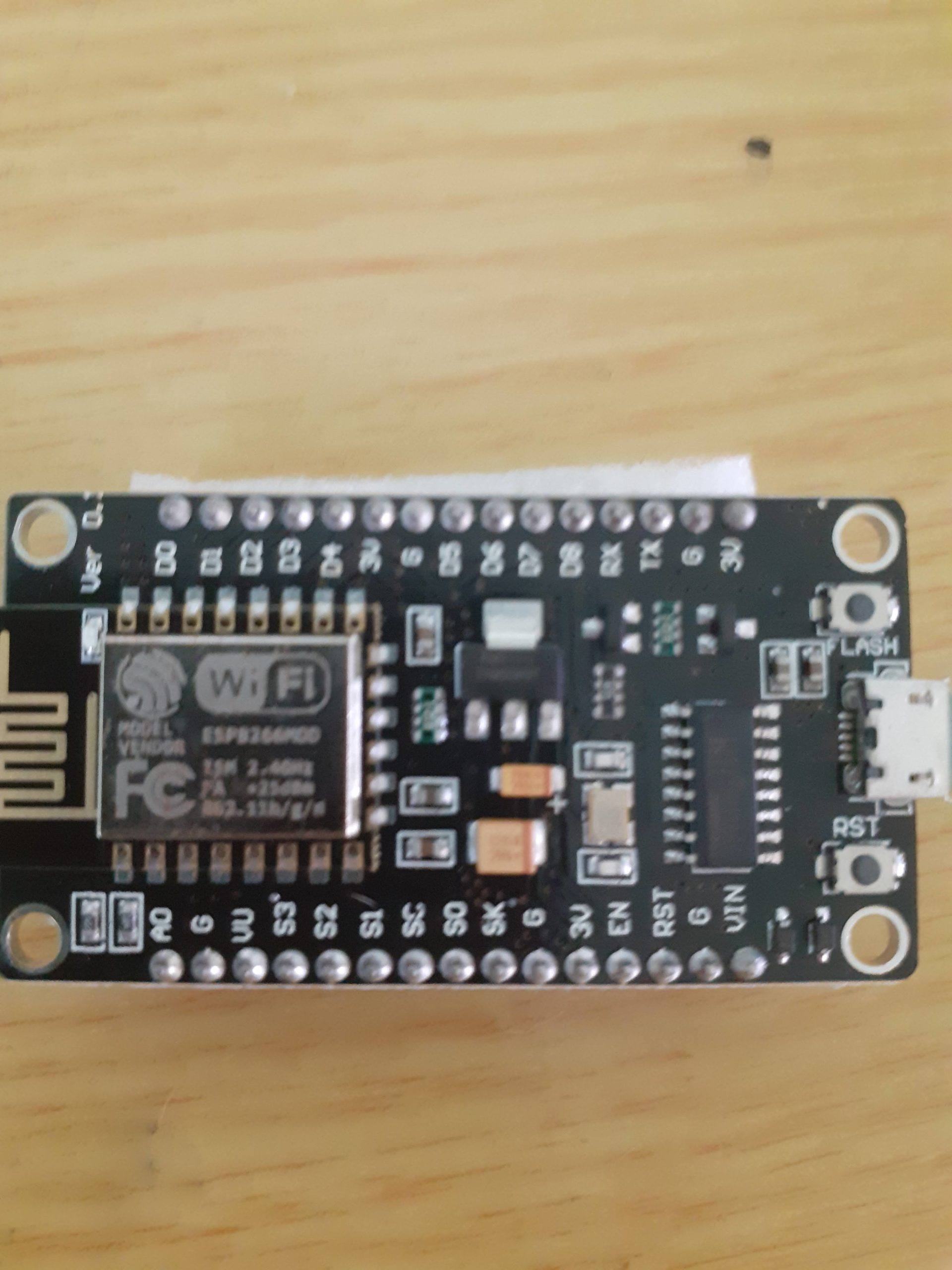
This post is getting quite long by now, so I have decided not to include my tests of the ESP-12E ( NodeMCU ) or ESP32 development boards here as well… They also function as expected.
In Summary
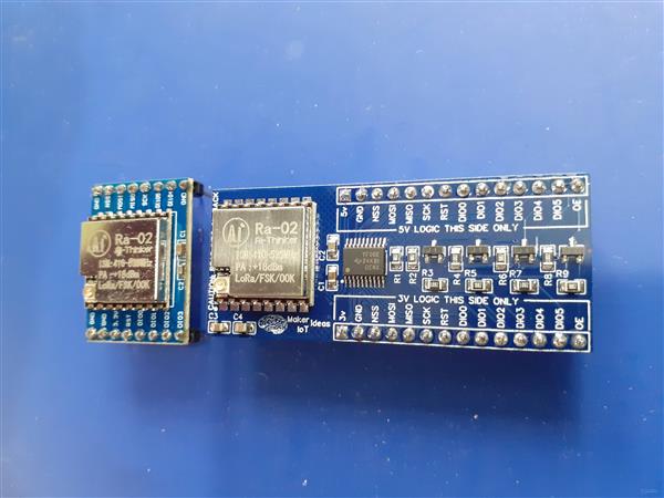
When I started this project, I set out to solve a problem ( personal to me ), that could potentially help a lot of other people use the RA-02 Module for more projects and tasks. The Breakout module in its current form can also be used with the RA-01h module (915Mhz Module) without any changes. All GPIO pins are broken out, and accessible through full logic converted pins on both sides of the breakout module.
I hope that this will be useful to someone. I am also not releasing the full schematics at this stage, as I may decide to make some minor cosmetic changes in the near future.
The PCB can however be ordered from PCBWay in its current form and works 100% as expected. The BOM file is available with the ordered PCB as usual.

This PCB was manufactured at PCBWAY. The Gerber files and BOM, as well as all the schematics, will soon be available as a shared project on their website. If you would like to have PCBWAY manufacture one of your own, designs, or even this particular PCB, you need to do the following…
1) Click on this link
2) Create an account if you have not already got one of your own.
If you use the link above, you will also instantly receive a $5USD coupon, which you can use on your first or any other order later. (Disclaimer: I will earn a small referral fee from PCBWay. This referral fee will not affect the cost of your order, nor will you pay any part thereof.)
3) Once you have gone to their website, and created an account, or login with your existing account,

4) Click on PCB Instant Quote

5) If you do not have any very special requirements for your PCB, click on Quick-order PCB

6) Click on Add Gerber File, and select your Gerber file(s) from your computer. Most of your PCB details will now be automatically selected, leaving you to only select the solder mask and silk-screen colour, as well as to remove the order number or not. You can of course fine-tune everything exactly as you want as well.


7) You can also select whether you want an SMD stencil, or have the board assembled after manufacturing. Please note that the assembly service, as well as the cost of your components, ARE NOT included in the initial quoted price. ( The quote will update depending on what options you select ).


8) When you are happy with the options that you have selected, you can click on the Save to Cart Button. From here on, you can go to the top of the screen, click on Cart, make any payment(s) or use any coupons that you have in your account.
Then just sit back and wait for your new PCB to be delivered to your door via the shipping company that you have selected during checkout.