What is a matrix keypad?
A matrix keypad is a type of keypad that uses a matrix of wires to connect the keys to the microcontroller. This allows for a smaller and more compact keypad than a traditional keypad, which uses a single row and column of wires for each key. Matrix keypads are also more reliable than conventional keypads, as they are less susceptible to damage from dirt and moisture.

How does a matrix keypad work?
A matrix keypad is made up of a number of rows and columns of keys. Each key is connected to two wires, one for the row and one for the column. When a key is pressed, it completes a circuit between the row and column wires. The microcontroller can then determine which key is pressed by checking which row and column wires are connected.
Why use a matrix keypad?
There are a number of reasons why you might want to use a matrix keypad in your project. Here are a few of the most common reasons:
- Smaller size and footprint.
- Reliability.
- Cost savings.
What makes my design different from most others out there?
While the matrix keypad in its simplest form is constructed from only wires and switches, that simple approach can sometimes have some unwanted effects, especially when pressing multiple keys at the same time – a phenomenon called ghosting – where you get phantom keypresses. This is easily eliminated by adding a diode in series with each switch, usually on the row connection.
That single component fixes ghosting reliably but does not come without its own problems, the most important of these being that a keypad with diodes becomes “polarised” – current can only flow in a single direction through a switch. This can cause problems with some third-party libraries, as the designer of the keypad and the designer of the library very often has quite different ideas of what a row and a column mean in a keypad.
This is important, – here we go down the rabbit hole; in my understanding of the keypad scanning routine, a column runs from top to bottom, and a row from left to right. Keeping this in mind, the microcontroller will alternatively set each column HIGH, and configure each row as an input. When a key is pressed, current will flow from the specific column GPIO, through the switch, and into the Row GPIO, sending the input pin HIGH…
It is also possible to configure the columns as inputs, with internal pullups enabled, and have each Row pin as an output, configured to sink ( pull current to ground). This will cause the specific column to go low – thus identifying the pressed key…
These different ways of handling the problem of reading a key, and believe me, there are actually more variations, create a few unique problems. We may have to swap rows and columns as far as pin connections and firmware are concerned, as well as define a custom “keymap” to assign values to each key.
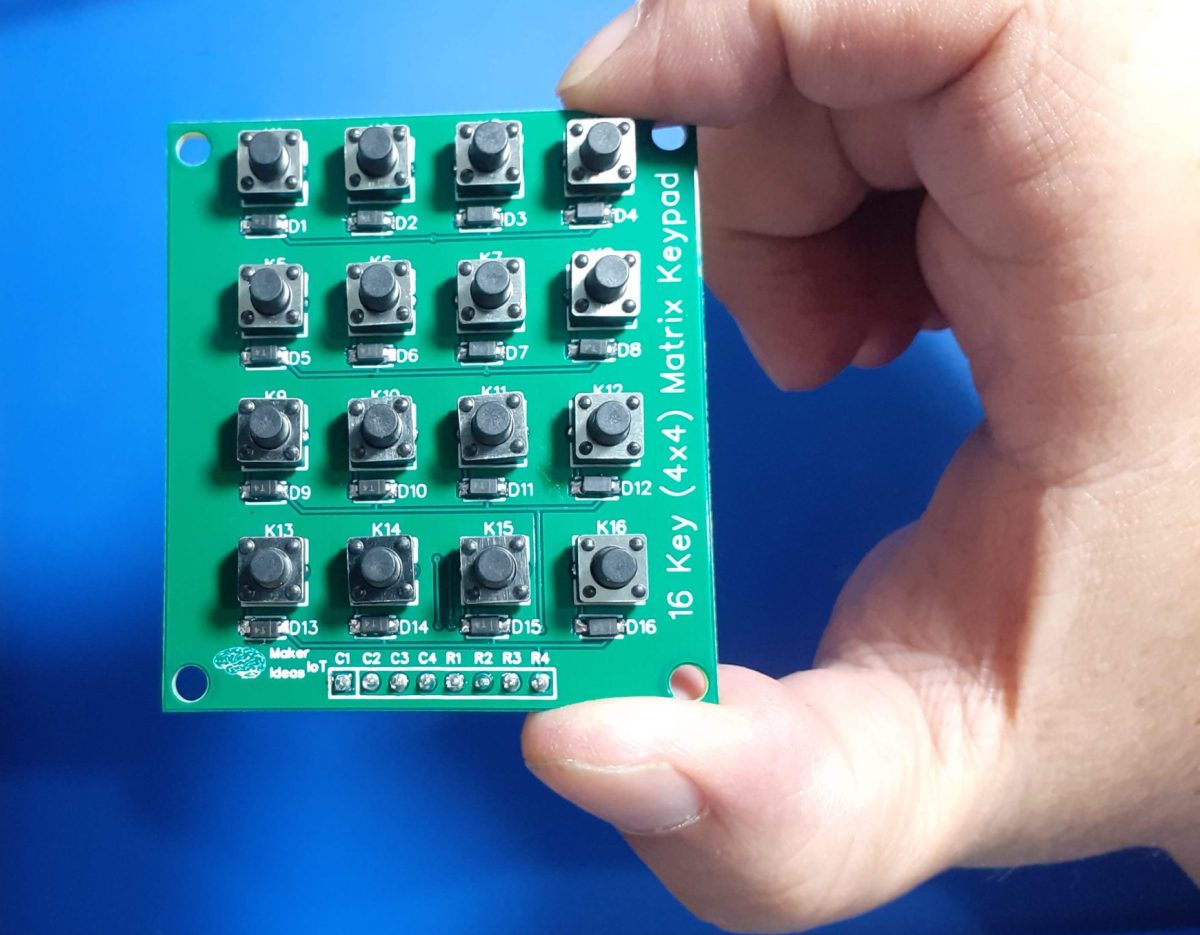
The Schematic

As we can see above, the schematic is very basic. 16 switches, 16 diodes and a single 8-way header pin. Pin 1 to 4 on the header is connected to Columns 1 to 4, and Pin 5 to 8 is connected to Rows 1 to 4.
The diodes prevent “ghosting currents from flowing into other keys in a row when multiple keys are pressed together. They also seem to help with other stray signals and interference.
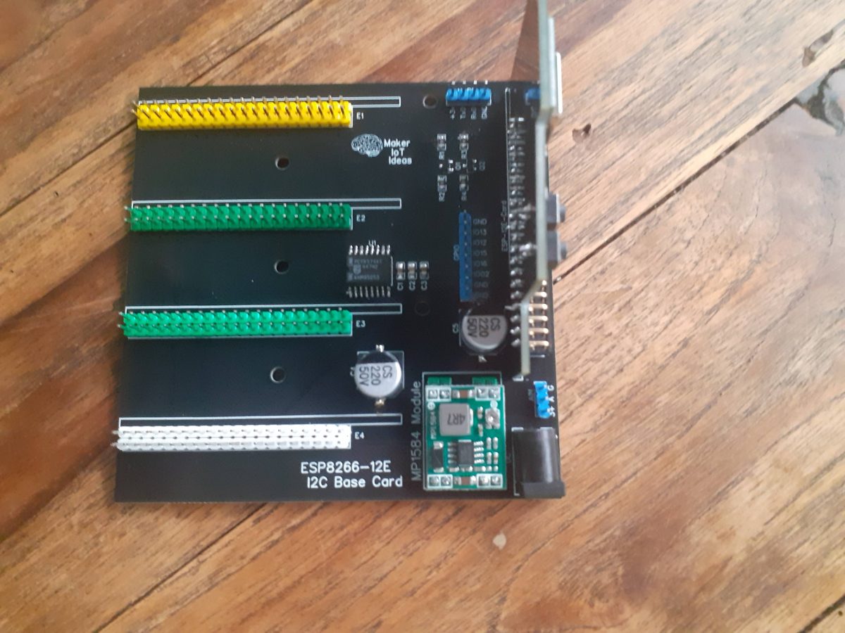
The PCB
The PCB is a simple double-layer board. All components are mounted on the top layer.

To limit interference from stray signals, I have routed rows and columns on opposite sides of the PCB where possible.
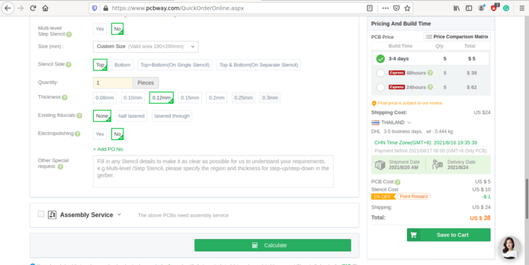
Manufacturing
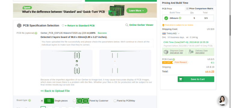
I choose PCBWay for my PCB manufacturing.
This month, PCBWay is also celebrating its 9th anniversary, and that means that there are quite a lot of very special offers available.
Why? What makes them different from the rest?
PCBWay‘s business goal is to be the most professional PCB manufacturer for prototyping and low-volume production work in the world. With more than a decade in the business, they are committed to meeting the needs of their customers from different industries in terms of quality, delivery, cost-effectiveness and any other demanding requests. As one of the most experienced PCB manufacturers and SMT Assemblers in China, they pride themselves to be our (the Makers) best business partners, as well as good friends in every aspect of our PCB manufacturing needs. They strive to make our R&D work easy and hassle-free.
How do they do that?
PCBWay is NOT a broker. That means that they do all manufacturing and assembly themselves, cutting out all the middlemen, and saving us money.
PCBWay’s online quoting system gives a very detailed and accurate picture of all costs upfront, including components and assembly costs. This saves a lot of time and hassle.
PCBWay gives you one-on-one customer support, that answers you in 5 minutes ( from the Website chat ), or by email within a few hours ( from your personal account manager). Issues are really resolved very quickly, not that there are many anyway, but, as we are all human, it is nice to know that when a gremlin rears its head, you have someone to talk to that will do his/her best to resolve your issue as soon as possible.
Find out more here

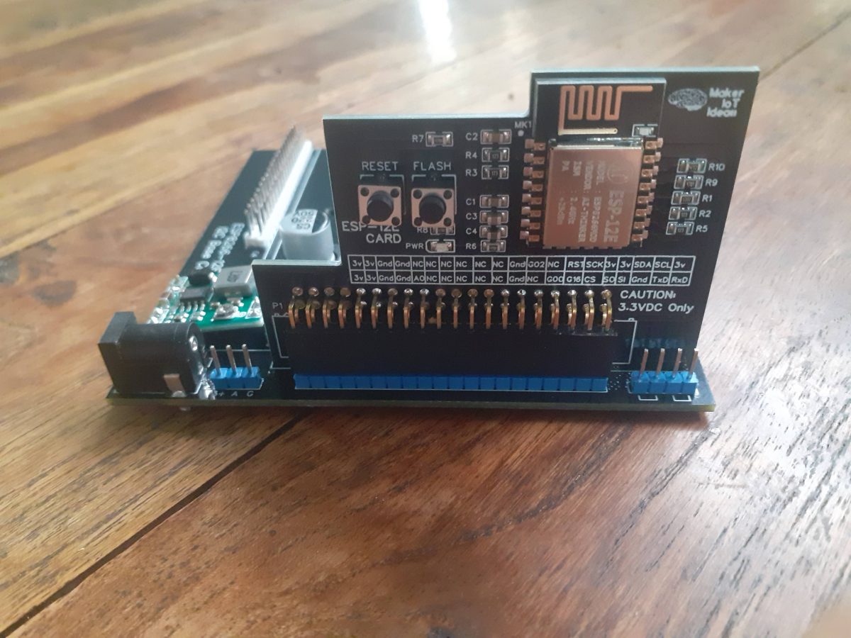
Assembly
This project does not require a lot of specialised equipment to assemble. The SMD diodes can easily be soldered by hand, the same with the switches and 8-way header. In my case, I chose to solder the header pins on the back of the PCB, that way, I can later use the keypad in a suitable enclosure without having wires in the way.


Testing and Coding
Testing a matric keypad can sometimes be a challenge. In my case, a multimeter with clip leads, set to diode mode, with the leads connected to each column and row in turn, while minding the polarity, and pressing each key in that row in turn, verified continuity.
With that done, it was time to put my trusted Cytron Maker Uno to work, as this Arduino Clone has the added benefit of having LEDs on each of the GPIO lines, thus making it very easy to see what is happening.
I made use of a Keypad library in the Arduino IDE, mainly to cut down on the amount of coding, but also because it is easier to use a working piece of code, and then adapt that to my keypad.
Detailed Code examples for ESPHome are available on Patreon
/* @file CustomKeypad.pde
|| @version 1.0
|| @author Alexander Brevig
|| @contact alexanderbrevig@gmail.com
||
|| @description
|| | Demonstrates changing the keypad size and key values.
|| #
Edited by MakerIoT2020, with minor changes to make it function correctly with my custom keypad.
I have also added a simple LED blinking routine to show that the Arduino is “alive” and that the Keypad code seems to be NON-blocking – which is quite important to me.
*/
#include <Keypad.h>
const byte ROWS = 4; //four rows
const byte COLS = 4; //four columns
//define the symbols on the buttons of the keypads
char hexaKeys[ROWS][COLS] = {
{‘1′,’4′,’7′,’*’},
{‘2′,’5′,’8′,’0’},
{‘3′,’6′,’9′,’#’},
{‘A’,’B’,’C’,’D’}
};
byte rowPins[ROWS] = {2,3,4,5}; //connect to the row pinouts of the keypad
byte colPins[COLS] = {6,7,8,9}; //connect to the column pinouts of the keypad
/*
* Due to libraries being written by different people, and our definitions about
* what a row and a column are, is different, note that the rows in the code
* is actually the columns on my PCB. This becomes true, due to the fact that my
* PCB has Diodes on each switch, and that thus makes current flow in only one
* direction///
*
* it also has the “side effect” that keys are layout in a strange “mirrored” and
* rotated way in the firmware.
* it does however NOT affect the correct operation of the Keypad Module at all
*
*/
const int LEDPin = LED_BUILTIN;
int ledState = LOW;
unsigned long prevmillis = 0;
const long interval = 1000;
//initialize an instance of class NewKeypad
Keypad customKeypad = Keypad( makeKeymap(hexaKeys), rowPins, colPins, ROWS, COLS);
void setup(){
Serial.begin(115200);
pinMode(LEDPin,OUTPUT);
}
void loop(){
unsigned long currentMillis = millis();
if (currentMillis – prevmillis >= interval) {
prevmillis = currentMillis;
if (ledState == LOW) {
ledState = HIGH;
} else {
ledState = LOW;
}
digitalWrite(LEDPin,ledState);
}
char customKey = customKeypad.getKey();
if (customKey){
Serial.println(customKey);
}
}
This code works very well and allowed me to verify the correct operation of the keypad.
In conclusion
Making my own Keypad Module is a project that is long overdue. I have purchased a few online over the years, and as they were mostly of the membrane type, they did not last very long – it must be something to do with the ultra-cheap flexible PCB ribbon connector, since a quality membrane keypad can be quite expensive, and usually lasts quite a long time.
Having my own module available to experiment with will allow me to do some long-delayed improvements to many of my IoT modules. That code, mostly YAML for ESPHome, will be made available on Patreon.