
Table of contents
Introduction
My Requirements
My Solution
Expandability
Prototyping
–> Initial Software Installation
—–> Start Home Assistant
—–> Install ESPHome
—–> Flashing ESPHome
–> Designing the Hardware
—–> The Relay Driver Circuit(s)
——–> Relay Driver Schematic
——–> Status LED and User Input Schematic
——–> The USB to Serial Schematic
——–> The ESP-12E schematic with strapping pins, as well as the power supply circuit(s)
—–> Designing the PCB
——–> PCB Layout (Raw layers and Silkscreen, not Rendered)
——–> Top Layer
——–> Bottom Layer
——–> 3D Render ( Top Layer from left )
—–> Manufacturing – PCBWay
—–> What to expect in Part 2
Introduction
The Internet of Things (IoT), as well as Home Automation, are steadily gaining popularity all the time. You can already buy quite a lot of commercial products or do your own D.I.Y implementation. Many different companies offer various devices and modules to help you do your project easily. But many of us will know that these modules always come with a lot of wires and connections, which can be very unreliable, and also unsightly to look at.
Most of these solutions are also relying on you placing some stuff on an electronics-breadboard, or strip-board for more permanent installations. You can also decide to design and manufacture your own custom PCB.
On the software side of this problem, there are many commercial and open-source solutions available, and most of them work with almost anything on the market (With various degrees of complexity and a varying learning curve).
Go back to the Table of Contents
My Requirement(s)
Having access to a few ( four to be exact ) Raspberry Pi Computers, as well as a huge number of ESP8266, ESP32, Arduino and STM32 Development boards that are lying around in my working area, as well as being quite lazy to do repetitive tasks, I have been playing with the idea for quite a while to automate some or maybe all of the lights in my house. I have also built quite a few device prototypes, only to tear them down again after testing them.
The reason for this, and this is only my own opinion, is that an electronics breadboard is meant for prototyping only.
They are not reliable in the long term, and they look extremely messy. Using a certain development board, and connecting all of the supporting components and modules to it, also leaves quite a mess. So,
1) The project must be contained on a single PCB.
2) It must have WiFi and or Bluetooth support (ESP8266 does not have this [ Bluetooth ])
3) It must be able to be powered from 220v mains directly, OR, through a single Plug Type AC to DC converter, preferably something already available on the market.
4) The power supply unit must supply adequate power to the unit.
5) I want to make some actual use of a Raspberry Pi, as they were not meant to lie around gathering dust 🙂
6) Once completed, the project should be able to be updated OTA or with as little fuss as possible.
7) The freedom to code in whatever language I want, as well as be easy to use with prebuilt firmware like ESPHome and or Tasmota and the likes.
Go back to the Table of Contents
My Solution (Hardware and Software)
Taking into consideration cost, as well as flexibility, I decided on using the ESP8266 and in later versions ESP32.
These have WiFi and Bluetooth already built-in but have a nasty breadboard form factor. The popular NodeMCU is a great starting point, but it has many small design flaws, most of which were fixed in later versions, but, as I live in SE Asia, and electronics are super cheap, you never know what you get.
With this in mind, I have decided to design my own controller, based on the ESP-8266 12E Module. This will give me the flexibility I need while allowing me to add custom components and features as needed, which is not possible with a stock version.
As far as Software is concerned, Home Assistant, running on a Raspberry Pi 4B with 4Gb Ram will be sufficient to control all of this. Firmware on the ESP12-E can be either ESPHome, Tasmota, or something that I write on my own, connecting to the internet and using MQTT for communication. (The options here are also almost too many to mention, but, IFTTT, Adafruit IO, and Blynx come to mind… Alexa and Google Assistant support are also possible, but definitely not required in my application at this moment.
Go back to the Table of Contents
Addon Hardware and Expandibility
Any permanent project grows on you, and over time, you will want to add features and functions. Keeping this in mind when you start designing saves a lot of headaches later. I will thus definitely make sure to provide access to the I2S, SPI and Serial Peripherals.
Prototyping and Initial Testing
Software
It is quite impossible to design something without building a prototype, and doing some very rigorous testing.
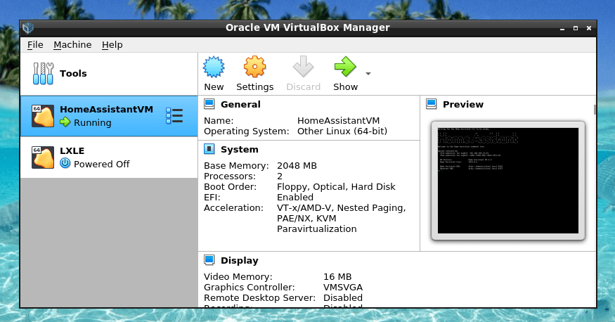
To do this, I have started with a copy of Home Assistant running in a VM on my HP ML350G Debian server computer. This way, I can quickly test Home Assistant, and make sure everything works as I want it to, without having to do it on the PI. This will mean that I will have to re-do most of the software configuration again on the PI,
but it gives me the flexibility to take snapshots and restore them if something goes wrong.
The procedure that I followed, for VirtualBox, can be found here. I am sure that it will be very similar for Windows users.
Start Home Assistant
When you have completed the installation, you can go ahead and start Home Assistant.
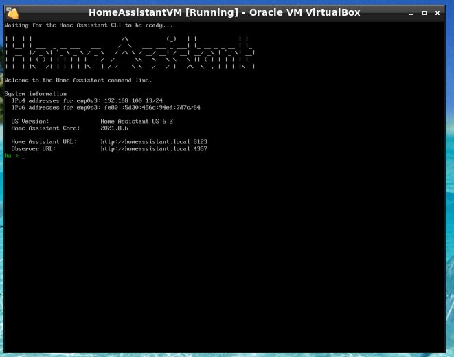
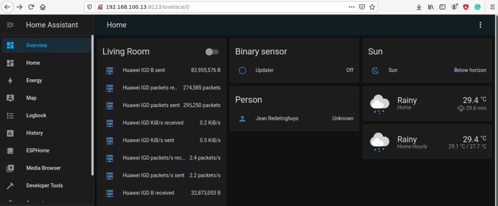
You may now open Home Assistant in your browser by going to http://<your-ip-address>:8123 and pressing enter.
You will see something similar to this:
Install ESPHome
You may now scroll down to the Supervisor Menu Item, Click on the Addon Store link, and Install ESPHome.
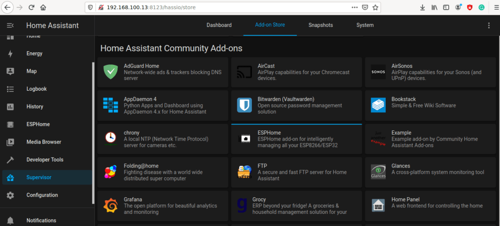
Please make sure that you select “start on boot”, “watchdog”, “auto-update” and “show in the sidebar”
Also, make sure to start the add-on
Go back to the Table of Contents
Flashing ESPHome to your device
You are now ready to flash ESPHome onto your development board. Please note that you will have to repeat this step on the actual PCB device that we will design and build later.
For now, we will however use a standard NodeMCU v3 module, as it contains the ESP-12E module that we require.
As we have not configured HTTPS in our Home Assistant installation, we can only flash the initial firmware using an external application. This application is called ESPHome Flasher, and you can download it here.
Prepare to Flash
We need to create an initial device in ESPHome. to do this, you need to click on the ESPHome Menu Item in the Home Assistant sidebar. Then click on the Green and White + sign at the bottom right corner…
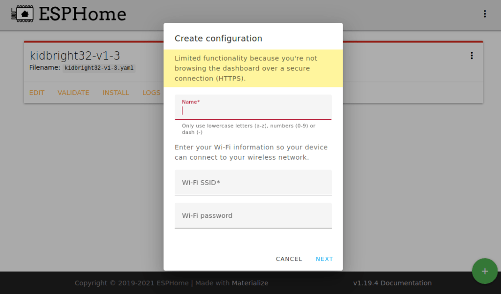
Give your device a descriptive name, I went with iot-con-prototype. Also, add your WiFi network credentials (SSID and Password). Then click on NEXT.
You now have to select your ESP board. I went with NodeMCU.
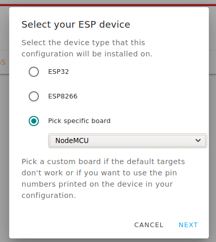
Click on NEXT when you are done.
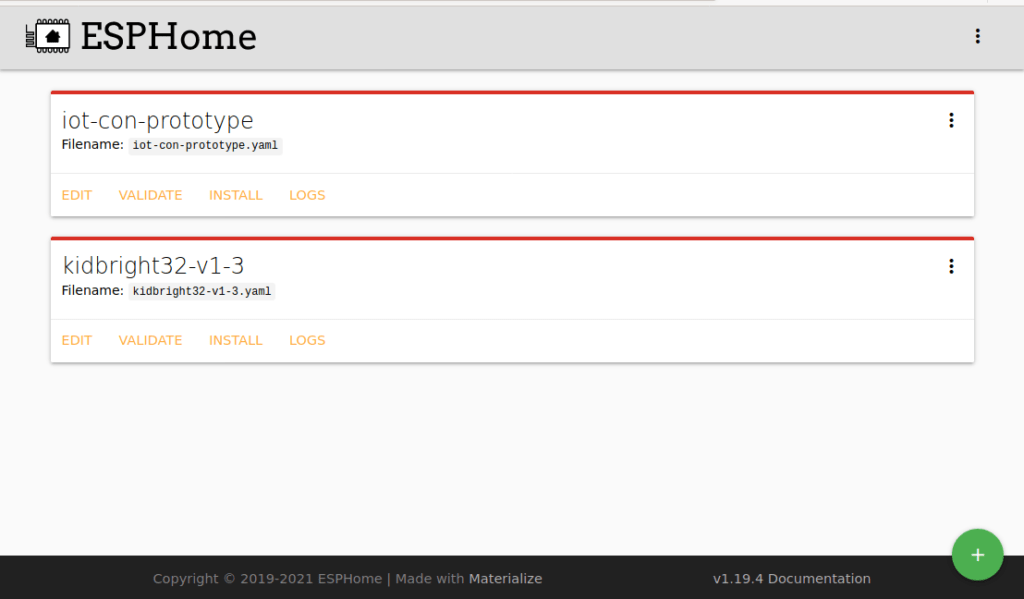
You will now be alerted that a configuration has been created. Click on the Close button.
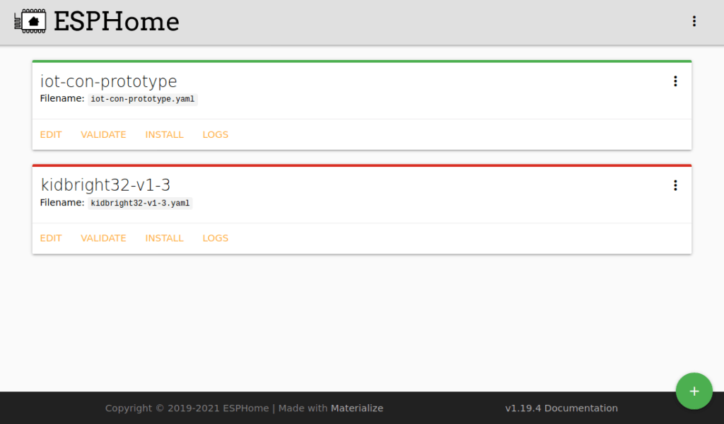
You will now see your device in the list. The red line means that the device is OFFLINE.
If you have not installed ESPHome Flasher yet, now is a good time to do it. When you are done, connect the NodeMCU module to the computer’s USB port and start ESPHome Flasher.
Note: On Linux, you dont have to install it. you can just start it from the terminal using
./ESPHome-Flasher-1.3.0-Ubuntu-x64.exec ( this example is for Debian ) yours may differ … sudo may be required
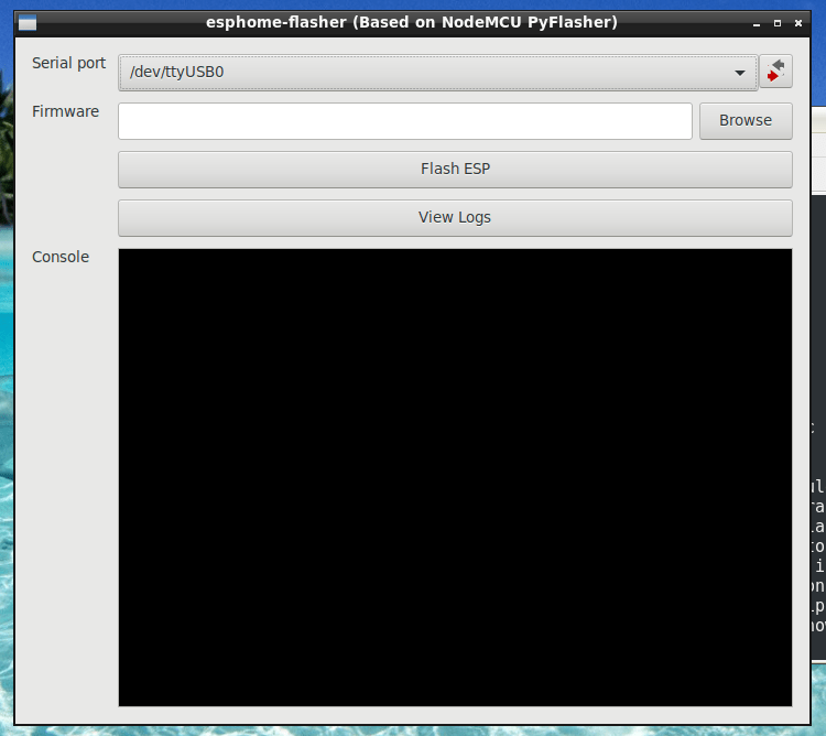
Select the communications port from the dropdown menu.
Now go back to Home Assistant, ESPHome Screen.
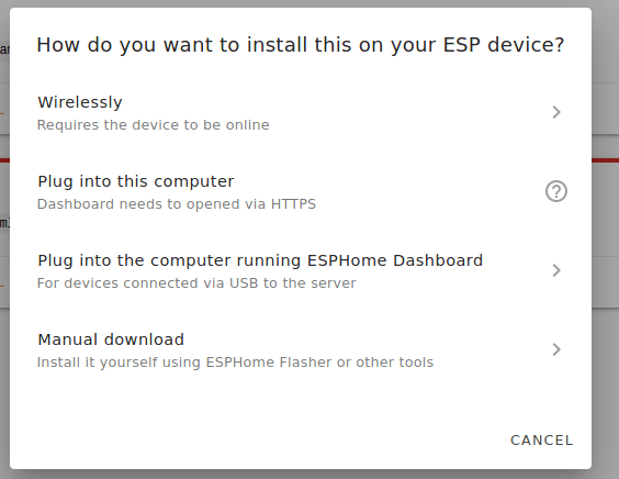
Click on the Install link (in yellow) of the device that we added previously.
Then click on Manual Download
ESPHome will now compile your initial firmware and prompt you to save the .bin file it has generated.
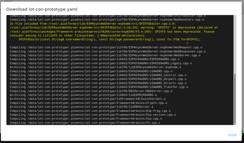
Take note of the location of this file, we will need it for the next step.
Now you can go back to the ESPHome Flasher window, and browse to the .bin file that you have just generated and downloaded.
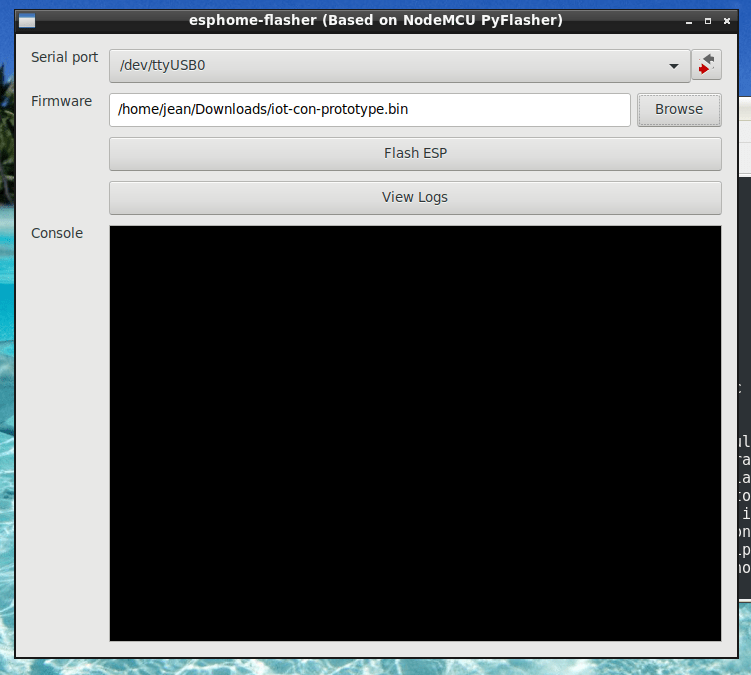
When this is done, you can click on Flash ESP. The firmware will now be flashed onto the NodeMCU device that we will use as our prototype.
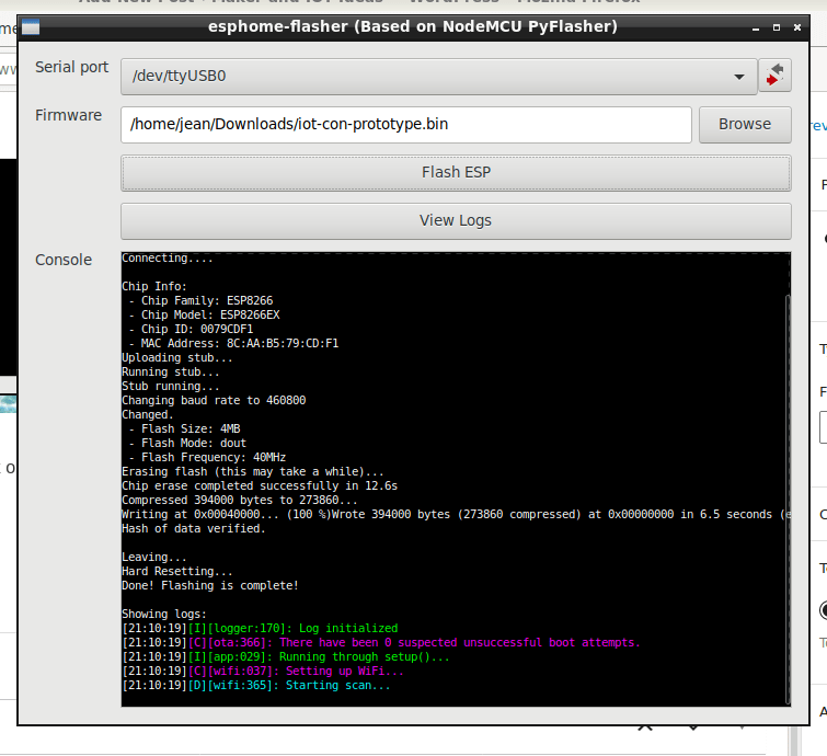
You can close the Flasher application when you see predominantly purple text in the console window. This means that the device has connected successfully with your WiFi network, and by extension, also with ESPHome and Home Assistant.
If you now go back to ESPHome, you will see that the device has a green line above its name, which means that it is online. Please note that at this stage, the device does not do anything, as we have not yet configured it. That will be our next task, but before we do that, we will have to start playing with some of the physical hardware yet.
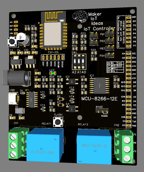
Designing the Hardware
I have decided to base this controller on the popular NodeMCU v3 development board. This little board makes use of the ESP12-E module, designed by AITinker, from whom I have bought many well-designed modules before. The module (NodeMCU) is in a BreadBoard form factor, and thus clearly meant for prototyping, or use on a base-board of some kind. I do however have some issues with this module, namely:
1. Many of these units are in fact clones. Some of these does not have proper protection between the board and the USB port to power them. This makes it dangerous to connect power to the VIN pin.
2. The board does not have a built-in 5v regulator. The 5v output (VIN) is thus taken directly from the USB port that powers it. This limits the total available current to the board and all peripherals to the 500mA available from the USB port.
All of these issues are however easy to overcome, as Espressif has made available excellent documentation on using their modules. I will thus be using this documentation as a reference design for my own device.
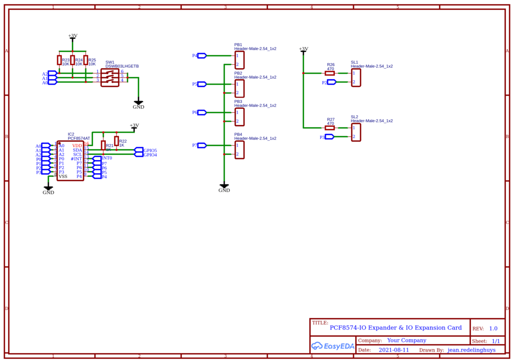
Another issue is expandability. The module provides many broken out GPIO pins (D0 to D8), but in order to remain super flexible for future expansion, I would have to make sure that I keep the built-in peripherals, like i2c, spi, and uart free for connection to external addon components in future. To solve this, I have decided on using the PCF8574 I2C IO Expander. This means that…
D0 (GPIO16) needs to be kept free for Wake up from deep sleep mode
D1 (GPIO5) SCL line of I2C Bus
D2 (GPIO4) SDA line of I2C Bus
D3 (GPIO0) connected to Flash Button, and also a strapping pin
D4 (GPIO2) Tx of UART 1
D5 (GPIO14) HSCLK – SPI Clock
D6 (GPIO12) HMISO – SPI MISO
D7 (GPIO13) Rx UART 2 / HMOSI – SPI MOSI
D8 (GPIO15) Tx UART 2 / HCS – SPI CS as well as a strapping pin
D9 ([Rx] GPIO03) Rx UART 0
D10 ([Tx] GPIO01) Tx UART 0
Looking at this, it is thus very clear that I2C is the way to go, as it will use only two pins, leaving the other GPIO’s free for future expansion.
Go back to the Table of Contents
Relay Driver Circuit, status led(s) and user control
The PCF8574 has very weak current sourcing capabilities, but it can sink 25mA per IO pin. As I will be driving the chip from 3v, this will however not be enough to drive a 5v relay. I will thus be making use of an optocoupler to drive the relay from 5v, using a general-purpose NPN transistor. That way, I can make sure that I do not overload the IO line on the PCF8574, as well as keep the 3v and 5v lines isolated from each other. (They will however still share a common ground).
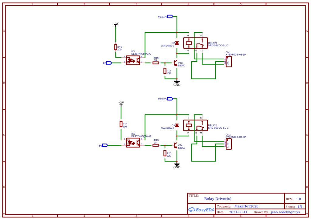
As you can see from the schematic above, the relay driver(s) will be connected to P0 and P1 of the PCF8574. A 200-ohm resistor will limit the current to about 16.5mA @ 3.3v. This is well within the tolerance of 25mA for the PCF8574 as well as the 50mA limit of the EL357N Optocoupler chip.
On the output side, I made use of the S8050 general purpose NPN transistor, capable of a 25v collector-emitter voltage, ant a continuous current of 500mA. Move than sufficient to drive the +/- 70mA to 80mA of current required by the relay coil. The current through the phototransistor side of the optocoupler is limited by a 1k resistor to the base of the transistor, to 5mA.
Go back to the Table of Contents
Provision is made for up to four (4) pushbuttons, by pulling pins P4 to P7 down to ground, through an external push-button connected to a 2-way pin header. The design allows for the pin to be used for another function as well, with an additional breakout pin provided on the edge of the board.
Likewise, the two status LED’s on P2 and P3 is connected via a 470-ohm resistor each, driving them at approximately 7mA each. This is once again within the 25mA sink limit of the PCF8574. These pins can also be used to connect to other hardware instead via the breakout header at the edge of the board.
The user input(s) and status led circuit was purposefully kept as plain as possible, as it is very likely that the additional 6 ports taken up by these will be used for other purposes instead.
USB to Serial Interface
The USB-to-Serial interface is done by using a CH340G. I have not modified the reference design from the original NodeMCU v3 too much, as it works well, and thus need no changes. I did however make sure that there is a protection diode between the USB 5v line and the VIN line on the PCB. Most of the existing NodeMCU boards does not do this, or when they do have the protection diode, that line is directly connected to the VIN pin. in my view, that is not ideal, and can cause unnecessary damage to your computer’s USB port or NodeMCU board in the event that you power it from an external source, and also use USB power to upload code… Not that it should be done that way anyway, but rather safe than sorry later.
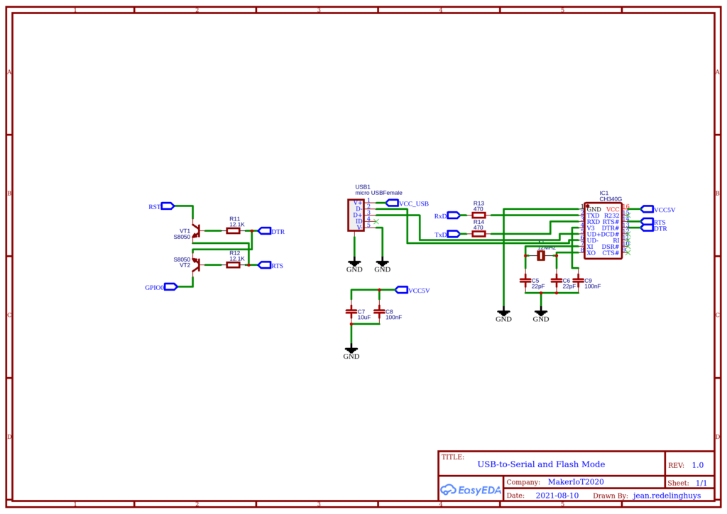
The two transistors (VT1, and VT2) is used to do very cleverly put the board into programming mode, as well as reset it after flashing, without the end-user having to press any of the flash or reset buttons. This is also part of the reference design on some of the NodeMCU boards. I can not comment if it is standard. I found it useful, so decided to include it as well.
ESP-12E with strapping pins and power supply
The ESP-12E module, as manufactured by AITinker, seems to be quite stable and easy to use. It does however have a couple of caveats, to enable it to function as intended. The strapping pins (discussed later) should be in a certain state at bootup time, and failure to adhere to that will definitely cause a failed boot or wrong startup mode.
GPIO0, GPIO2, EN and RST should be pulled HIGH for a NORMAL boot, while GPIO15 should be pulled LOW.
Pulling GPIO0 LOW at boot, will put the board into FLASH mode.
Another change that I made is that I did not break out the raw Analog input pin, as is done on some of the boards ( as a VV pin, or sometimes as an unlabeled, or reserved pin). The Analog input pin on the stock module is designed for around 1.0v input. This is fed from a resistor divider, to effectively scale your 5v input down to valid levels.
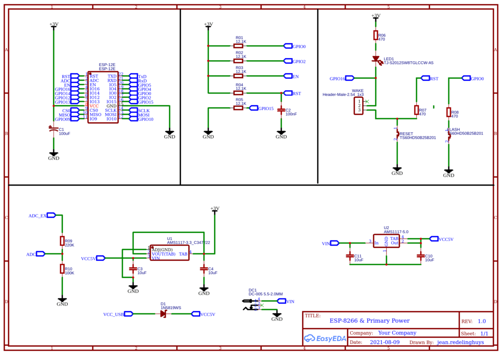
GPIO16 (D0) is used internally by the ESP-12E to wake the module from deep sleep. This is done by connecting GPIO16 to the reset pin. To wake up the module, GPIO16 is internally pulled LOW, thereby resetting the module.
I have decided to add a user-selectable jumper that can be enabled to connect GPIO16 to RESET, that enabling this functionality. It is however to be noted that the jumper must ONLY be set AFTER the relevant deep sleep mode has been enabled in the firmware for the module.
The standard NodeMCU has only a single 3.3v voltage regulator installed. I added a dedicated 5v voltage regulator as well and powered it directly from the VIN pin. This regulator will only function when the device is powered from an external power source, with an upper voltage limit of 15v DC. Protection for the USB port is provided by a diode between VCC_USB and VCC5V.
Go back to the Table of Contents
Designing the PCB
As I have mentioned at the start of the article, this is a show and tell, of how I solved a particular problem that I had.
I do not believe in re-inventing the wheel, but to adapt and improve as and where I see fit, to my own purpose. This project will by no means be unique, or better or worse than other similar devices on the market today. It is however designed to suit my particular needs for my particular project.
The design of the PCB and Schematics was done in EasyEDA, which I believe to be quick and easy to use, as well as Linux friendly. (There does not seem to be many of those around, KiCAD being the exception to that rule. I have however not been too successful in using that before, to no fault of KiCAD at all. I am just not prepared to learn a new EDA CAD package just for the sake of doing it. Time is precious, and I can get everything I need to do done with EasyEDA).
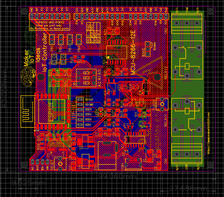
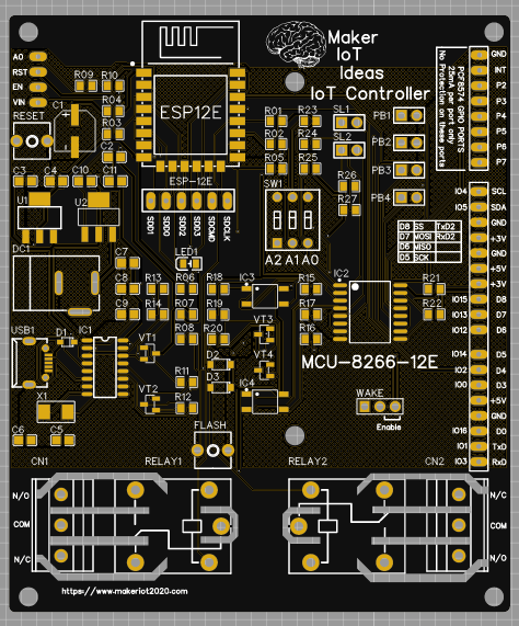
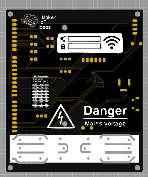
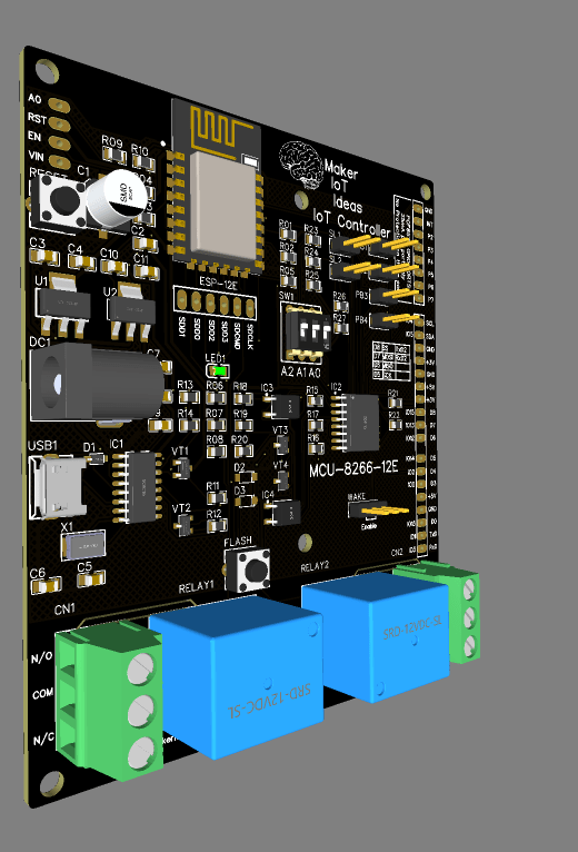
The PCB is dual-layer 99.06mm x 83.058mm. Six mounting holes are provided. The ESP-12E is placed at the top,
roughly in the left-hand corner. As per Espressif design recommendations, no tracks are routed underneath the antenna area. An approximate 15mm x Board width area is also kept clear of any tracks or ground plane(s) to also prevent interference with the RF signal generated by the device. All components are mounted on the top payer of the PCB and are as far as possible grouped together by their function and purpose in the circuit. As the two onboard relay modules will very likely be used to switch mains power, they have also been excluded from the ground plane(s). Cutouts around all possible mains power carrying pads and tracks were also added to prevent tracking.
A DC Power Socket, and USB port, as well as access to the single Analog Input, Enable, Reset Pin and Button and VIN pin is provided on the left-hand side of the PCB. All other IO pins, as well as the six remaining ports on the PCF8574 IO expander, is accessible on the right. Note that GPIO4 and GPIO5 ( D1 and D2 ) were hard-wired as I2C lines. They should thus not be used for any other purpose. All other pins are accessible and broken out, clearly labelled with their GPIO numbers, as well as NodeMCU style Dx numbers. There are also an additional 6 IO pins broken out at the bottom of the ESP-12E module, to provide access to the seldom-used SDCard interface.
Manufacturing the PCB
This PCB will be manufactured at PCBWAY. The Gerber files and BOM, as well as all the schematics, will soon be available as a shared project on their website. If you would like to have PCBWAY manufacture one of your own, designs, or even this particular PCB, you need to do the following…
1) Click on this link
2) Create an account if you have not already got one of your own.
If you use the link above, you will also instantly receive a $5USD coupon, which you can use on your first or any other order later. (Disclaimer: I will earn a small referral fee from PCBWay. This referral fee will not affect the cost of your order, nor will you pay any part thereof.)
3) Once you have gone to their website, and created an account, or login with your existing account,
4) Click on PCB Instant Quote
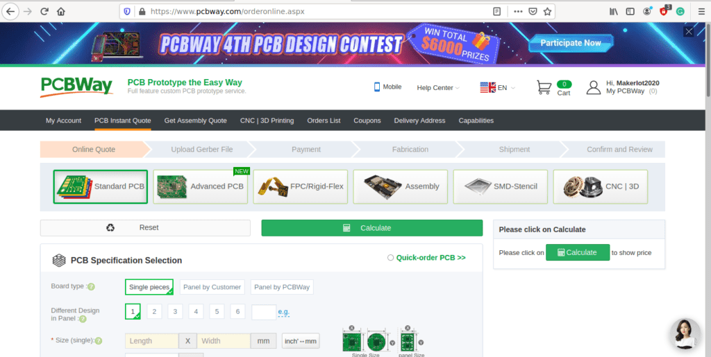
5) If you do not have any very special requirements for your PCB, click on Quick-order PCB
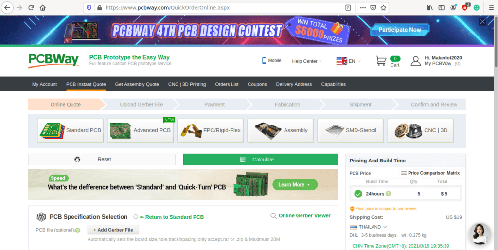
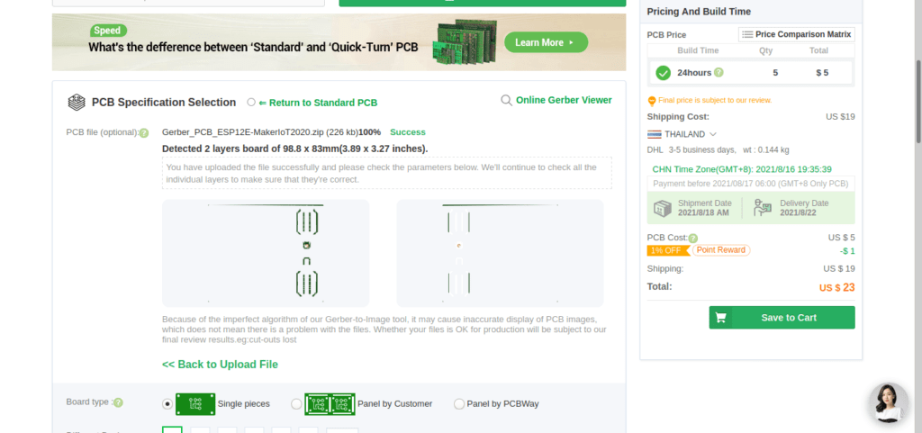
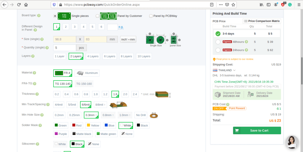
6) Click on Add Gerber File, and select your Gerber file(s) from your computer. Most of your PCB details will now be automatically selected, leaving you to only select the solder mask and silk-screen colour, as well as to remove the order number or not. You can of course fine-tune everything exactly as you want as well.
7) You can also select whether you want an SMD stencil, or have the board assembled after manufacturing. Please note that the assembly service, as well as the cost of your components, ARE NOT included in the initial quoted price. ( The quote will update depending on what options you select ).
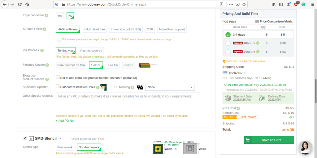
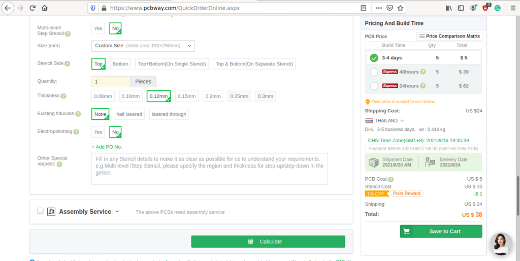
8) When you are happy with the options that you have selected, you can click on the Save to Cart Button. From here on, you can go to the top of the screen, click on Cart, and make any payment(s) or use any coupons that you have in your account.
Then just sit back and wait for your new PCB to be delivered to your door via the shipping company that you have selected during checkout.
Conclusion of Part 1
This is the end of a very long part 1. We have started to look at the steps involved to get started with designing our own IoT Controller, did some initial software installation, and took a detailed look at the schematics and PCB…
In part 2, we will look at
1) Writing the configuration for ESPHome to control your device
2) Look at Tasmota as an alternative way to control the device
3) Integrating the device into Home Assistant
4) Have a go at writing our own firmware using the Arduino IDE to control the device using MQTT
5) Depending on how long shipping of the components and PCB takes, assembly and testing of the actual device
Thank you for your time. This is a very long article, and I appreciate your interest.
Go back to the Table of Contents