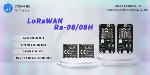
The Ai-Thinker company in Shenzen has recently introduced two new LoRa radio modules, the Ra-08 and Ra-08H. These new LoRaWAN modules are based on the ASR Microelectronics ASR6601 module featuring a 48MHz ARM Cortex M4 microcontroller and Semtech SX1262 transceiver allowing long-range, low power communication for the Internet of Things.
Both LoRaWAN modules share most of the same specifications, but the Ra-08 module operates in the 410-525MHz frequency band, while the Ra-08H module works in the widely used 803MHz to 930MHz band. Ai-Thinker also provides a development kit for each module.
Ai-Thinker Ra-08/Rs-08H key features and specifications:
Programmable embedded Arm Cortex-M4 MCU with 128 KB of Flash and 16 KB of SRAM
Power Consumption – Down to 0.9uA in deep sleep mode
Dimensions – 16 x 16 x 3.2m (SMD-18 package)
The modules support OTA firmware updates, and the company also provides PDF documentation for the individual modules, as well as Ra-08-kit and Ra-08H-kit development kits. Most of the documents are however still in Chinese, but can easily be translated with Google translate to make them easily understandable.
The modules feature a factory-installed AT-Command set for rapid application development, as well as the capability to completely reprogram the ARS6601 with your own custom firmware, using STMCube IDE from ST Microelectronics. At the moment, there does not seem to be any STMDuino support available for these, but we are sure that will change in the near future, as they gain popularity with users.
Applications
The Ra-08/08H modules, and ASR6601 LoRaWAN chip, enable a new generation of indoor and outdoor IoT applications such as smart agriculture, smart cities, smart meters, asset tracking, streetlights, parking sensors, smoke sensors, smart environmental monitoring, automation in the smart home, building automation, and more.
If you’d like to find out more, or order samples, please check out the Ai-Thinker website or contact them by email at overseas@aithinker.com.
Special Offer MakerIoT2020 has two sets of Ra-08 and RA-08H development kits available for two lucky readers, limited to one set each. These modules are unused and brand new from the factory. Find out more on our Facebook and Instagram pages on how to stand a chance to get them for free (shipping to your own account)
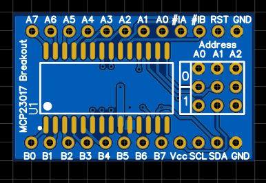
I2C port extenders or expanders are extremely useful devices, and I use quite a lot of them in my projects. My go-to device is definitely the PCF8574, mainly because it is sort of “breadboard friendly”. The MCP23017, with the existing breakouts available locally, are not. I have thus decided to design my own version of a breadboard friendly MCP23017 breakout board.
The Breakout Module PCB and its features
A breadboard friendly MCP23017 breakout board – Fronta breadboard friendly MCP23017 breakout board – Back
While this was definitely one of my easier projects, It still took a bit of time to get it just right and add some essential components and features directly onto the PCB.
The main features of this breakout: – DIP12 Layout – with all pins broken out, address pins to jumper headers… – Proper decoupling capacitors, as close as possible to the MCP23017 chip. I had to make use of the back layer of the PCB to do this, not exactly ideal, but with proper power and ground planes, and nice thick tracks, I believe they will be just fine.
– Address selector jumpers – The breakouts that are available locally, do not have these. – Breadboard friendly layout – 33.020mm x 20.320mm [board size], with 15.240mm vertical spacing between the rows of pins, ensures that you can easily fit it onto your breadboard, while still having space to add jumper wires to the pins. Horizontal pin spacing is standard 2.45mm.
The Schematic
The schematic is plain and simple. A few points to note though: – The address selection header, as well as the io pin headers are not shown on the schematic. – I2C pullup resistors are set at 1k but can be replaced with more suitable values as required in your circuit
The PCB for this project is currently on its way from China, after having been manufactured at PCBWay. Please consider supporting them if you would like your own copy of this PCB, or if you have any PCB of your own that you need to be manufactured.
If you would like to have PCBWAY manufacture one of your own, designs, or even this particular PCB, you need to do the following… 1) Click on this link 2) Create an account if you have not already got one of your own. If you use the link above, you will also instantly receive a $5USD coupon, which you can use on your first or any other order later. (Disclaimer: I will earn a small referral fee from PCBWay. This referral fee will not affect the cost of your order, nor will you pay any part thereof.) 3) Once you have gone to their website, and created an account, or login with your existing account,
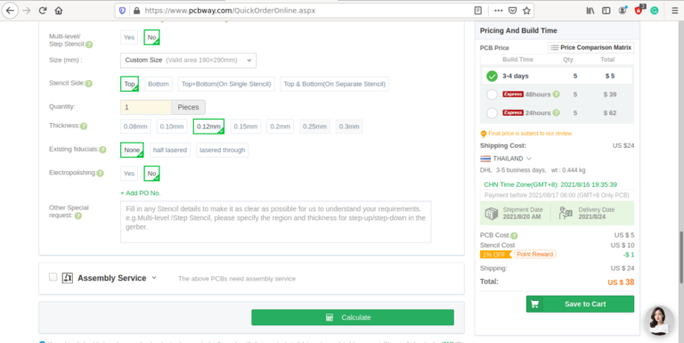
4) Click on PCB Instant Quote
5) If you do not have any very special requirements for your PCB, click on Quick-order PCB
6) Click on Add Gerber File, and select your Gerber file(s) from your computer. Most of your PCB details will now be automatically selected, leaving you to only select the solder mask and silk-screen colour, as well as to remove the order number or not. You can of course fine-tune everything exactly as you want as well.
7) You can also select whether you want an SMD stencil, or have the board assembled after manufacturing. Please note that the assembly service, as well as the cost of your components, ARE NOT included in the initial quoted price. ( The quote will update depending on what options you select ).
8) When you are happy with the options that you have selected, you can click on the Save to Cart Button. From here on, you can go to the top of the screen, click on Cart, make any payment(s) or use any coupons that you have in your account.
Then just sit back and wait for your new PCB to be delivered to your door via the shipping company that you have selected during checkout.
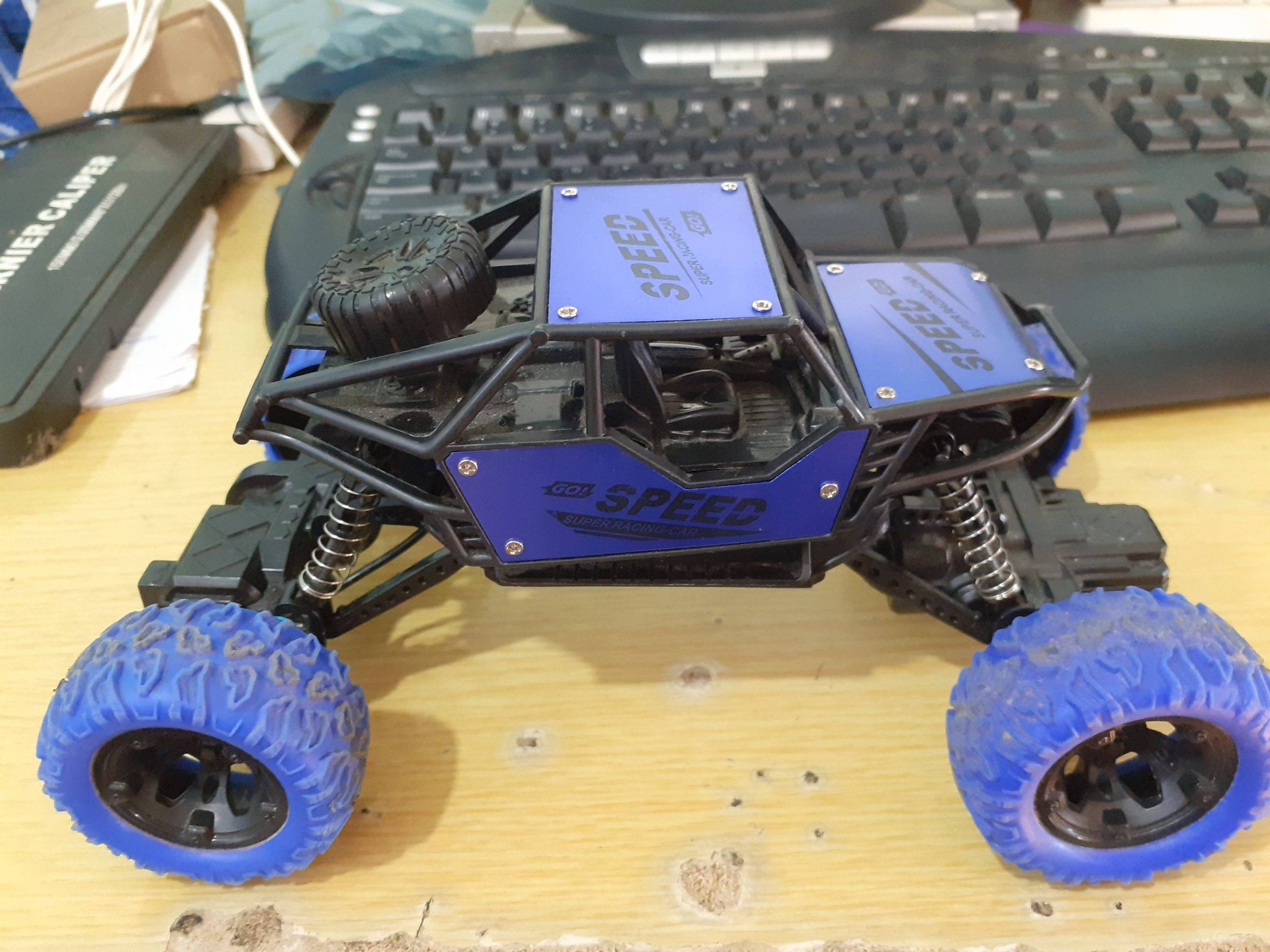
Many of us have old toys laying around the house, they belong to our children or the children of our friends. In this article, I will attempt to show you how to give an old toy car new life, as well as hopefully teach a child a few interesting things with electronics.
The inspiration for this article comes from my friend’s 7-year-old boy, who, way too clever for his age, always has a lot of very interesting questions. His mother and I have thus decided to do an experiment: “Let us try to teach him Arduino programming, so he can start to make his own toys”
Obviously, the challenges in this venture are many… To name a few: The boy speaks only Thai, so English is a no-go. Soldering is out of the question, due to his age, as well as safety issues – All teaching will have to be done on a breadboard.
My challenges apart, this is a project that many people would want to attempt, so it is important to start with a bit of theory.
Controlling a DC Motor from a microcontroller
DC motors, like those found in toy cars, are inductive loads, and that means that they induce electromagnetic fields when switched on or off. These EMF fields can damage your sensitive microcontroller quite easily. Another thing to remember is that your typical microcontroller can only source or sink in the region of 25mA to 50mA of current, not quite enough to drive a motor, let alone a toy car.
Directional control of the motor
In our toy car, we would definitely want the driving motor to be able to change direction, meaning spin forwards or backwards, thereby changing the direction that the car is travelling. This is achieved by using a circuit called an H-Bridge. In this circuit, four transistors, either BJTs or MOSFETs are arranged in a particular way to allow us to change the direction that the motor spins by changing certain logic signals.
Implementing an H-Bridge with switches
In the picture above, we simulate the H-Bridge circuit using slide switches in order to explain the method of operation. It should be clear that the direction is changed by switching on diagonally opposite switches.
Driving a motor with a transistor
In the picture above, we implement a simple, one-directional motor control circuit using a single transistor. This circuit still has the limitation that the motor can only spin in a single direction.
Half of an H-Bridge
In the circuit above, we combine the two motor driver circuits (with PNP and NPN transistor ) to complete one half of the H-Bridge circuit. This circuit still has the limitation that we can only spin the motor in a single direction.
The completed H-Bridge circuit
In the picture above, we added another half H-Bridge to complete the circuit. We will thus have 2 PNP and 2 NPN transistors, which form the completed circuit. This circuit will give us full bi-directional control of the motor. We can also control the speed of the motor if we apply a suitable PWM signal to the bases of the NPN transistors – we do need to be careful of SHOOT THROUGH and shorts though.
My proposed Motor Driving Circuit
the inside of the toy car, without the old broken circuit-board
In the picture above, we can clearly see that there is not a lot going on inside this toy car. An On-Off switch is connected to the battery compartment, and two wires go to the drive- and steering motor.
Interfacing this car to a microcontroller is thus going to require two separate H-Bridge circuits. One for the drive motor, and the second for the steering.
Dual H-Bridge Circuit diagram
I have designed the circuit above to control both motors of the toy car, the control signals are simplified to 2 per H-Bridge, and a common PWM signal to control speed.
Manufacturing the PCB
The PCB for this project is currently on its way from China, after having been manufactured at PCBWay. Please consider supporting them if you would like your own copy of this PCB, or if you have any PCB of your own that you need to be manufactured.
If you would like to have PCBWAY manufacture one of your own, designs, or even this particular PCB, you need to do the following… 1) Click on this link 2) Create an account if you have not already got one of your own. If you use the link above, you will also instantly receive a $5USD coupon, which you can use on your first or any other order later. (Disclaimer: I will earn a small referral fee from PCBWay. This referral fee will not affect the cost of your order, nor will you pay any part thereof.) 3) Once you have gone to their website, and created an account, or login with your existing account,
4) Click on PCB Instant Quote
5) If you do not have any very special requirements for your PCB, click on Quick-order PCB
6) Click on Add Gerber File, and select your Gerber file(s) from your computer. Most of your PCB details will now be automatically selected, leaving you to only select the solder mask and silk-screen colour, as well as to remove the order number or not. You can of course fine-tune everything exactly as you want as well.
7) You can also select whether you want an SMD stencil, or have the board assembled after manufacturing. Please note that the assembly service, as well as the cost of your components, ARE NOT included in the initial quoted price. ( The quote will update depending on what options you select ).
8) When you are happy with the options that you have selected, you can click on the Save to Cart Button. From here on, you can go to the top of the screen, click on Cart, make any payment(s) or use any coupons that you have in your account.
Then just sit back and wait for your new PCB to be delivered to your door via the shipping company that you have selected during checkout.
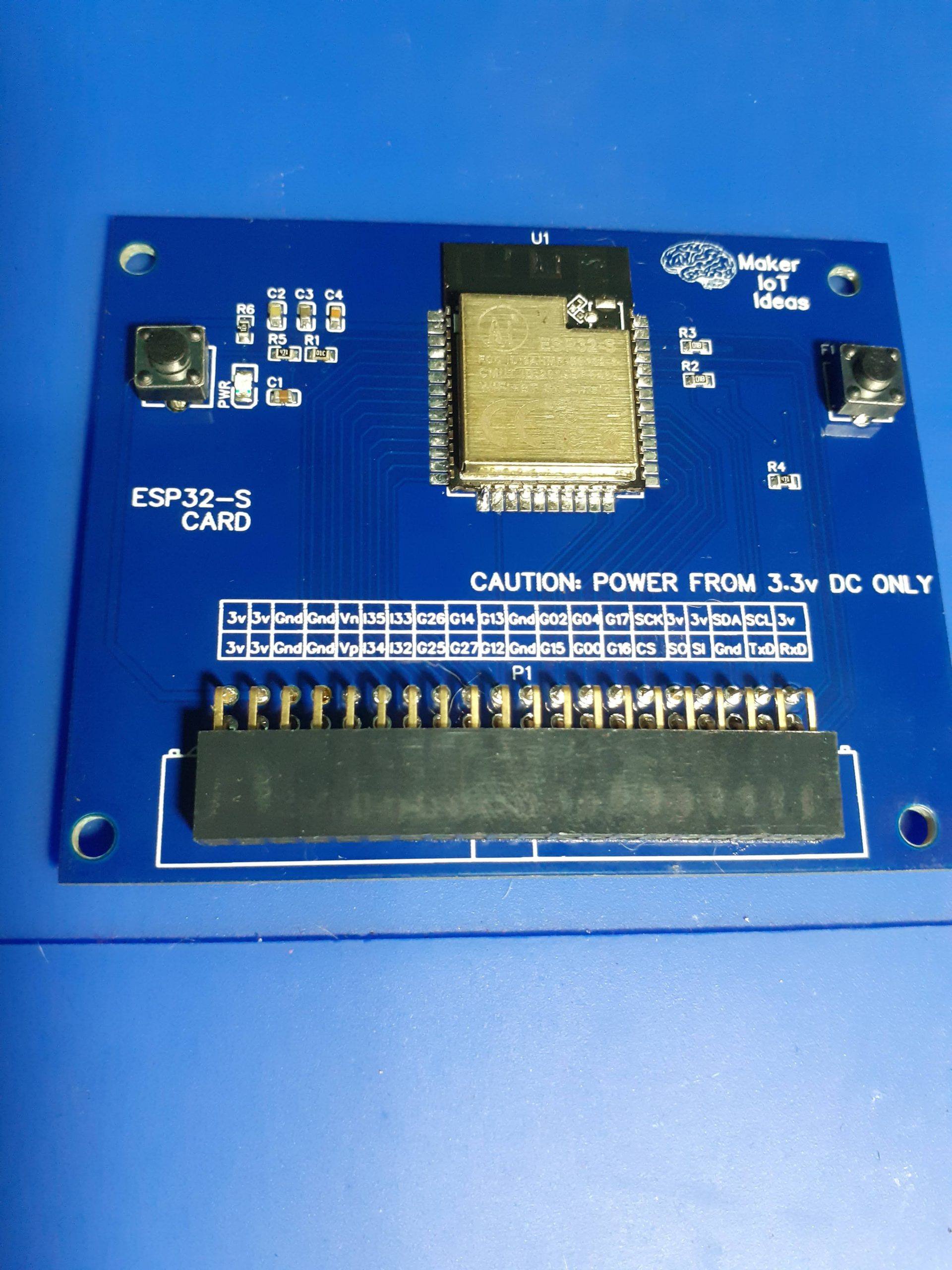
This project is the result of a lot of prototyping, using different MCUs and wanting to find a way to get a standard interface to all the devices.
The idea is to eventually create similar card-type MCU breakout boards, with similar pins in the same position on the 2x20p breakout header,
for example, power, i2c bus, reset and flash will always be in the same position on the female header…
Step 2 from here on would be to design a baseboard, that is capable of providing power, as well as access to the various GPIO pins. I am thinking along the way of a PC motherboard style interface, with “slots” at regular intervals. These “slots” will have access to the SPI, and I2C bus, as well as various other GPIO.
Step 3 would be a series of commonly used input and output “cards” that will plug into the “slots”…
If successful, I plan to design various MCU cards, with various different processors, with the obvious criteria that they are 3v powered.
This could result in a very flexible development platform, where it is possible to reuse the base-board and IO “cards” with any one of the various MCU “cards”.
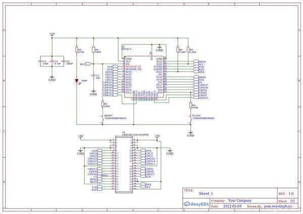
The Schematic
As seen on the schematic, almost all of the ESP32-S’s pins are broken out, with the exception of those used for internal flash. Reset and Flash circuitry is provided on the PCB, as well as on the 2x20pin female header.
It is worth noting that I did not include any UART to USB circuitry on the card. Flashing should be performed with an external USB-to-UART converter. It will however be included in the base-board.
There is also no power supply circuitry onboard. This was also intentional, as the card is intended to be powered from the base-board. It is however perfectly acceptable to power only the card from a suitable 3.3v DC power supply unit through the 3v and gnd pins on the 2x20pin header.
Where can I get my own version of this module?
This module will be exclusively available from PCBWay for the foreseeable future. Click on this link to order your own, and help support a great company that produces very high-quality PCBs for a very affordable price.
This PCB was manufactured at PCBWAY. The Gerber files and BOM, as well as all the schematics, will soon be available as a shared project on their website. If you would like to have PCBWAY manufacture one of your own, designs, or even this particular PCB, you need to do the following… 1) Click on this link 2) Create an account if you have not already got one of your own. If you use the link above, you will also instantly receive a $5USD coupon, which you can use on your first or any other order later. (Disclaimer: I will earn a small referral fee from PCBWay. This referral fee will not affect the cost of your order, nor will you pay any part thereof.) 3) Once you have gone to their website, and created an account, or login with your existing account,
4) Click on PCB Instant Quote
5) If you do not have any very special requirements for your PCB, click on Quick-order PCB
6) Click on Add Gerber File, and select your Gerber file(s) from your computer. Most of your PCB details will now be automatically selected, leaving you to only select the solder mask and silk-screen colour, as well as to remove the order number or not. You can of course fine-tune everything exactly as you want as well.
7) You can also select whether you want an SMD stencil, or have the board assembled after manufacturing. Please note that the assembly service, as well as the cost of your components, ARE NOT included in the initial quoted price. ( The quote will update depending on what options you select ).
8) When you are happy with the options that you have selected, you can click on the Save to Cart Button. From here on, you can go to the top of the screen, click on Cart, make any payment(s) or use any coupons that you have in your account.
Then just sit back and wait for your new PCB to be delivered to your door via the shipping company that you have selected during checkout.
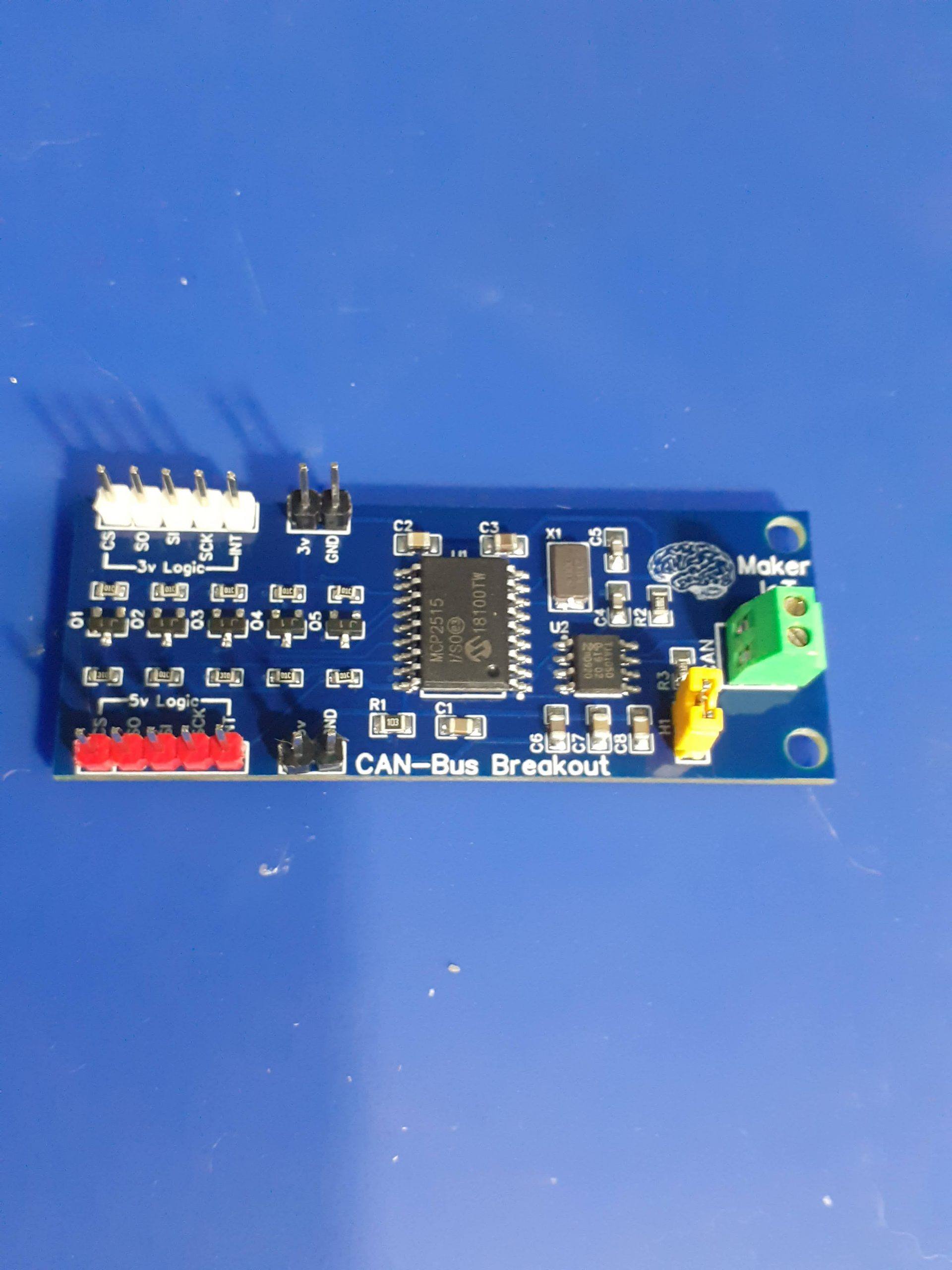
There are many CAN-Bus modules available for purchase to the DIY Electronics Enthusiast and the Maker community. Our Level Converted CAN-BUS module is different. Where the standard modules are all 5v devices, ours are level converted, allowing you to interface it with 3v and 5v microcontrollers, the choice is yours…
Level converted CAN-Bus ModuleLevel Converted CAN-BUS Module together with standard CAN-BUS breakout for comparison.
The Schematic
How does it work? / How do I use it?
The Level Converted CAN-BUS Module is based on the MCP2515 CAN Controller from Microchip, with the TJA1050 CAN Tranceiver used for communicating with the CAN-Bus. These two chips are extremely cheap and easy to get hold of, but they are also one of the main reasons for the redesign of the module.
While the MCP2515 is useable with a voltage range of 2.5v to 5v, the TJA1050 is not. When using the commercially available CAN-Bus modules, this limits you to using 5v microcontrollers, or for the more informed, using level converters in-between to translate back and forth to the desired logic levels.
The MCP2515 is an SPI device, and in my opinion, having long wires on an SPI bus is not always the best way of doing things, due to ringing and other undesirable interference. Having to add a level converter module into this already questionable setup, can add a lot of other undesirable effects.
I have thus decided to design and manufacture my own module, with 5 level converters directly on the PCB, thus reducing the length of connecting wires, as well as reducing complexity.
Using the device is now as easy as providing a 5v voltage source, as well as an additional 3v source if you need the level converters, and connecting your microcontroller to the appropriately marked logic side of the module.
A jumper at H1 can be set/unset to enable the 120ohm ballast resistor that is needed on the CAN-Bus for very short distance connections.
Example connection to an Arduino
Use the 5v logic side, and power the module with 5v and ground. You do not need a 3v power source. Connect the pins as follows:
CS pin to Arduino Pin 10 SO to the MISO pin on the Arduino Pin 12 SI to the MOSI pin on the Arduino, Pin 11 SCK to the SCK pin on the Arduino, Pin 13 INT to an interrupt capable pin on the Arduino, usually pin 2 or 3
Example connection to an ESP32 module
Provide a 5v as well as 3v power source with a common ground connection. Connect your logic to the 3v logic side of the PCB Module.
CS pin to GPIO2 SO to the MISO pin, GPIO19 SI to the MOSI pin, GPIO23 SCK to the SCK pin, GPIO18 INT to an interrupt capable pin on the ESP32
Where can I get my own version of this module?
This module will be exclusively available from PCBWay for the foreseeable future. Click on this link to order your own, and help support a great company that produces very high-quality PCBs for a very affordable price.
This PCB was manufactured at PCBWAY. The Gerber files and BOM, as well as all the schematics, will soon be available as a shared project on their website. If you would like to have PCBWAY manufacture one of your own, designs, or even this particular PCB, you need to do the following… 1) Click on this link 2) Create an account if you have not already got one of your own. If you use the link above, you will also instantly receive a $5USD coupon, which you can use on your first or any other order later. (Disclaimer: I will earn a small referral fee from PCBWay. This referral fee will not affect the cost of your order, nor will you pay any part thereof.) 3) Once you have gone to their website, and created an account, or login with your existing account,
4) Click on PCB Instant Quote
5) If you do not have any very special requirements for your PCB, click on Quick-order PCB
6) Click on Add Gerber File, and select your Gerber file(s) from your computer. Most of your PCB details will now be automatically selected, leaving you to only select the solder mask and silk-screen colour, as well as to remove the order number or not. You can of course fine-tune everything exactly as you want as well.
7) You can also select whether you want an SMD stencil, or have the board assembled after manufacturing. Please note that the assembly service, as well as the cost of your components, ARE NOT included in the initial quoted price. ( The quote will update depending on what options you select ).
8) When you are happy with the options that you have selected, you can click on the Save to Cart Button. From here on, you can go to the top of the screen, click on Cart, make any payment(s) or use any coupons that you have in your account.
Then just sit back and wait for your new PCB to be delivered to your door via the shipping company that you have selected during checkout.
Battery Backup for your Pi Zero (W) is a very important feature to prolong the life of the SD Card. Many commercially available solutions exist, in the form of Hats, but, unfortunately, it seems that anything that was specifically designed for the Raspberry Pi, can be quite expensive.
The 40 pin header on our Raspberry Pi Zero / Zero W gives us a lot of potentials to expand the functionality of this tiny single-board computer, but it, unfortunately, suffers from two major flaws, from my point of view of course.
The pins are scattered all over the place, and not grouped by function. Access to the pins is also very cluttered, to keep the overall footprint of the board small.
The GPIO pins are 3v only; adding anything that runs on a different voltage becomes a messy assembly of wires and level converters and or resistor dividers… going to a breadboard…
My Solution
Solving these issues required a lot of deep thinking, it actually took me a few months, during which I looked at various commercial solutions, imagined things in my mind, as well as tested concepts and various modules.
Let us take a look at some of these before I show you the solution that I am currently working on.
Battery Power
I would like to use a single 18650 LiPo cell to power the Pi Zero. Other Battery Backup solutions make use of this as well. In the ideal world, a pair of these in parallel would be great. The 18650 cell is a 3.3 volt ( nominal 4.2v) LiPo cell. The Pi needs 5v to run. This would require a Boost converter, as well as a dedicated LiPo charging circuit to recharge the cell after use.
Many such charging and Boost converters are available, but they seem to suffer from a problem, they need a dedicated charging cycle, during which using the device is not advised.
I could design my own circuit, but as I do not consider myself a proficient power supply designer, and with the huge amount of professionally designed, low-cost modules available, I decided to use the MH CD-42 module instead.
This module seems to give me all the features I need, with only one exception: The input voltage MUST be between 5.0v and 5.5v. I hope to address that issue later though.
It can source up to 2A at 5v, and most importantly, has a current bypass function, which allows you to charge the battery, as well as power an external device at the same time.
GPIO Pin Grouping and Level Conversion
The next logical step was to design a base-board that contained the 18650 Cell, and power module, as well as provide access to the GPIO pins.
I decided to use a 90 degree 2×20 pin Female header to mount the Pi, allowing for plenty of airflow around it to prevent overheating, as well as clearly labelled header pins for access to the GPIO pins. ( Due to logistics issues, the female header pin has not arrived yet).
The logic level conversion was provided on some of the GPIO ( SPI0, SPI1, I2C and UART ) by using the TXS0108E 8Ch Bidirectional Level Shifter chip from TI. Headers in black are 3v ( with exception of GPIO13) and 5v logic pins are on a white header.
Additional Ground and Power headers for 5v and 3v (red headers) were also added. Finally, a dedicated shutdown button was connected to GPIO26.
Schematic
Testing the prototype
The prototype is still under testing, as mentioned above, I still have to receive the 40 pin female header. I did however connect the Pi Zero to the board with jumper wires ( 3v, 5v and ground only ) to test operation. So far, the setup provides 5 hours of battery backup with the Pi on idle, no external devices connected and running only an MQTT server on Raspberry Pi Lite OS ( No Gui )
The first revision of the device is available for order at PCBWay
Manufacturing the PCB
This PCB was manufactured at PCBWAY. The Gerber files and BOM, as well as all the schematics, will soon be available as a shared project on their website. If you would like to have PCBWAY manufacture one of your own, designs, or even this particular PCB, you need to do the following… 1) Click on this link 2) Create an account if you have not already got one of your own. If you use the link above, you will also instantly receive a $5USD coupon, which you can use on your first or any other order later. (Disclaimer: I will earn a small referral fee from PCBWay. This referral fee will not affect the cost of your order, nor will you pay any part thereof.) 3) Once you have gone to their website, and created an account, or login with your existing account,
4) Click on PCB Instant Quote
5) If you do not have any very special requirements for your PCB, click on Quick-order PCB
6) Click on Add Gerber File, and select your Gerber file(s) from your computer. Most of your PCB details will now be automatically selected, leaving you to only select the solder mask and silk-screen colour, as well as to remove the order number or not. You can of course fine-tune everything exactly as you want as well.
7) You can also select whether you want an SMD stencil, or have the board assembled after manufacturing. Please note that the assembly service, as well as the cost of your components, ARE NOT included in the initial quoted price. ( The quote will update depending on what options you select ).
8) When you are happy with the options that you have selected, you can click on the Save to Cart Button. From here on, you can go to the top of the screen, click on Cart, make any payment(s) or use any coupons that you have in your account.
Then just sit back and wait for your new PCB to be delivered to your door via the shipping company that you have selected during checkout.
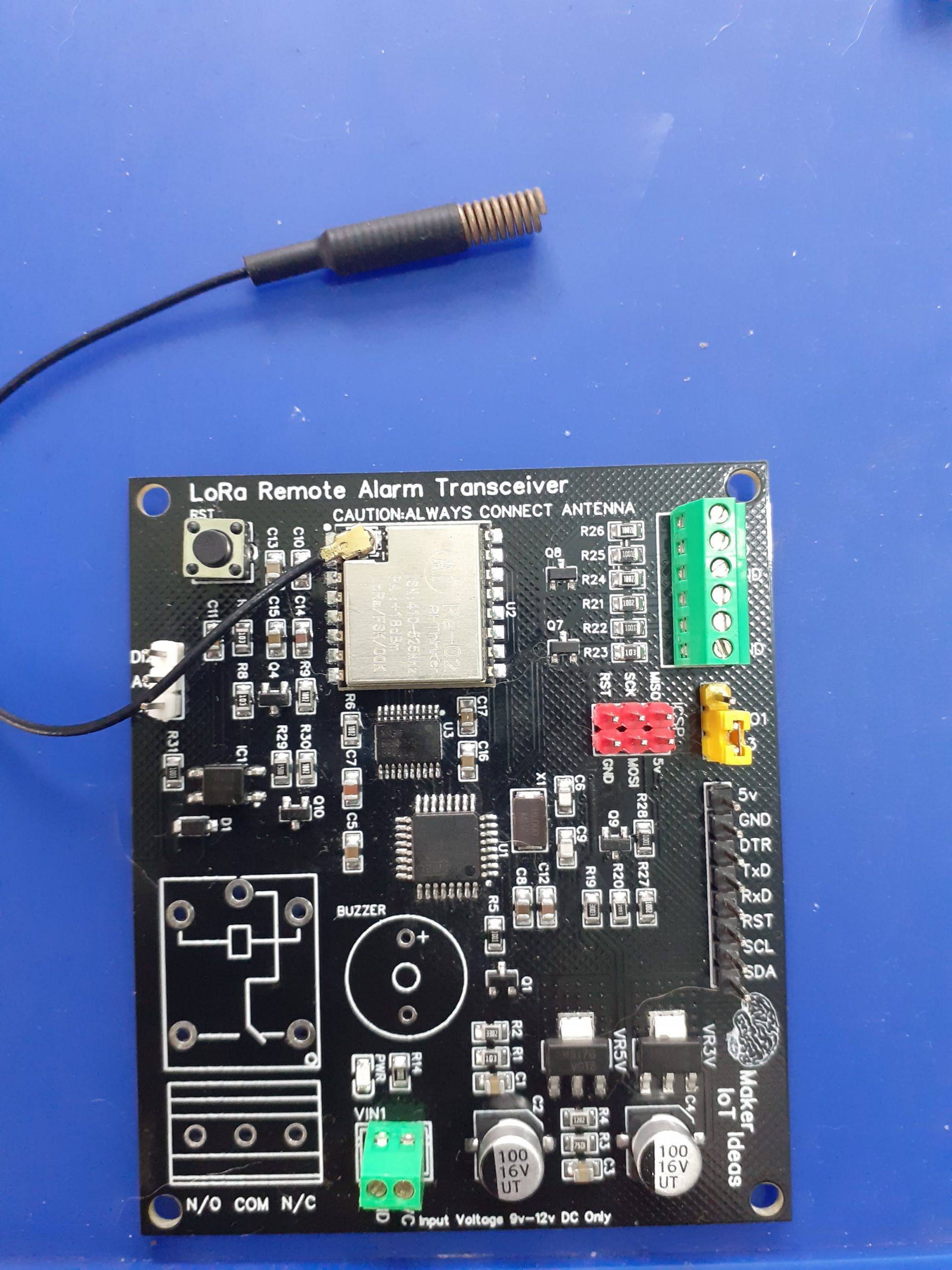
In part one of this series, I took a look at some of my experiments using different voltage regulators, to design and build the Remote Alarm Transceiver prototype, and also mentioned that I will be looking at a single chip logic converter solution. In this (hopefully short) post, I will take a detailed look at that logic converter chip, as well as show you how it is used.
Some of the features of the device is listed below:
• AEC-Q100 Qualified for Automotive Applications – Device Temperature Grade 1: –40°C to 125°C – Device HBM ESD Classification Level 2 – Device CDM ESD Classification Level C6 • No direction-control signal needed • Maximum data rates – 110 Mbps (push pull) – 1.2 Mbps (open drain) • 1.4 V to 3.6 V on A port and 1.65 V to 5.5 V on B port (VCCA ≤ VCCB) • No power-supply sequencing required – either VCCA or VCCB can be ramped first • Latch-up performance exceeds 100 mA per JESD 78, Class II • ESD protection exceeds JESD 22 (A Port) – 2000-V human body model (A114-B) – 1000-V charged-device model (C101) • IEC 61000-4-2 ESD (B port) – ±8 kV contact discharge – ±6 kV Air-gap discharge
Datasheet description:
This device is an 8-bit non-inverting level translator that uses two separate configurable power-supply rails. The A port tracks the VCCA pin supply voltage. The VCCA pin accepts any supply voltage between 1.4 V and 3.6 V. The B port tracks the VCCB pin supply voltage. The VCCB pin accepts any supply voltage between 1.65 V and 5.5 V. Two input supply pins allows for low Voltage bidirectional translation between any of the 1.5 V, 1.8 V, 2.5 V, 3.3 V, and 5 V voltage nodes. When the output-enable (OE) input is low, all outputs are placed in the high-impedance (Hi-Z) state. To ensure the Hi-Z state during power-up or power-down periods, tie OE to GND through a pull-down resistor. The minimum value of the resistor is determined by the current-sourcing capability of the driver.
Typical Application:
Reference Design / Typical Application for the TXS0108E
My Thoughts:
I really like the tri-state (high impedance) mode of the chip, as it allows for isolation between the different voltage level circuits, for example, If I were to communicate on a 5v SPI bus, to another device, I can for instance put the chip in Tri-state mode, and not worry about stray signals interfering from the 3v side.
On the downside, the chip is very small, which makes it a real challenge to solder by hand. On the speed side, It is also not quite as fast as my usual MOSFET based circuitry. It does however do the job it was designed for quite well.
Updated Circuit
Integrating the chip into the existing Remote Alarm Transceiver circuit is very easy, allowing us to replace almost all of the Mosfet-based Logic level converters. We do still need a few of them, as we have only 8 bidirectional channels on the TXS0108.
Schematics
Some Notes on the schematics:
A battery level monitor is connected through a voltage divider, with a MOSFET as a switch to the A0 pin. The voltage divider is set up for a 12v DC input source. The MOSFET is controlled from the D6 Pin.
The reason that I did this is, that I found some parasitic voltage leakage through the A2D converter in a previous design, reducing battery life. My hope is that by only reading battery level when the MOSFET is on, there can be an increase in battery life ( Taking into consideration that the Voltage regulators are not very efficient, it won’t really amount to a big gain unless I switch to an SMPS in the future. )
The PCB
The PCB
In the picture above, we can see the completed PCB (The relay and buzzer were not populated yet)
Manufacturing the PCB
This PCB was manufactured at PCBWAY. The Gerber files and BOM, as well as all the schematics, will soon be available as a shared project on their website. If you would like to have PCBWAY manufacture one of your own, designs, or even this particular PCB, you need to do the following… 1) Click on this link 2) Create an account if you have not already got one of your own. If you use the link above, you will also instantly receive a $5USD coupon, which you can use on your first or any other order later. (Disclaimer: I will earn a small referral fee from PCBWay. This referral fee will not affect the cost of your order, nor will you pay any part thereof.) 3) Once you have gone to their website, and created an account, or login with your existing account,
4) Click on PCB Instant Quote
5) If you do not have any very special requirements for your PCB, click on Quick-order PCB
6) Click on Add Gerber File, and select your Gerber file(s) from your computer. Most of your PCB details will now be automatically selected, leaving you to only select the solder mask and silk-screen colour, as well as to remove the order number or not. You can of course fine-tune everything exactly as you want as well.
7) You can also select whether you want an SMD stencil, or have the board assembled after manufacturing. Please note that the assembly service, as well as the cost of your components, ARE NOT included in the initial quoted price. ( The quote will update depending on what options you select ).
8) When you are happy with the options that you have selected, you can click on the Save to Cart Button. From here on, you can go to the top of the screen, click on Cart, make any payment(s) or use any coupons that you have in your account.
Then just sit back and wait for your new PCB to be delivered to your door via the shipping company that you have selected during checkout.
As part of my experiments with LoRa and the easy to use ATMega328P, I have recently designed quite a few LoRa based projects. In this final 2 part series, I will look at two additional projects, part of a Remote Alarm Transceiver, where I experimented with a changing a few things:
– Using LM317G adjustable voltage regulators. – Replacing my standard N-MOS based logic level converters with a dedicated chip.
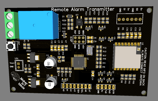
LoRa Remote Alarm Transmitter – with Onboard Relay putout and two sensor inputs
How does this differ from my other LoRa Based projects?
The PCB presented above does in fact not really differ a lot from any of my existing LoRa based projects. However, there are a few subtle changes, mainly experimental changes, brought on by factors such as component availability and an attempt to reduce component counts and board size.
The first of these changes is using the LM317G voltage regulator, in the place of my usual LM1117 3.3 and 5.0 LDO regulators.
The LM317 is an old device, It has been on the market for a long time. It can supply up to 1.5A of current, and a single device can be configured to supply a wide range of different voltages by just changing two resistors. This seemed quite attractive to me, as it is getting quite difficult to reliably get quite a few components on time, and with decent pricing in the post-Covid-19 world.
The second major change would be moving away from my existing N-Mos based Logic converter setup, where I used the BSS138 and 10K resistors as logic converters. This setup works perfectly, but it has the drawback of requiring quite a lot of components. for example:
To provide logic conversion to an RA-02 module, with access to all the IO Lines (GPIO0-5 included) required 12 BSS138 Mosfets and 24 10k resistors. This is quite a lot of components. A dedicated logic converter chip would thus be a much more attractive solution.
Driver circuitry for sensor Inputs, consisting of a simple transistor input, and an optically isolated Relay output completes the circuit.
Using the LM317
The output voltage of the LM317 is typically set using two resistors, with a suitable current rating, using the following Formula
VOUT = 1.25 * ( 1 + R2/R1 )
It is also common to use a variable resistor at R2, to have fine control over the output voltage. This is due to the fact that stock resistor values do not always give you the exact voltage you require. You should also take into account that using a 5% resistor will be less accurate than a 1% resistor.
The grid below is a list of common stock resistor values for R1/R2, with the resulting voltage produced.
R1 vs R2 Grid for use in selecting fixed output voltage
R2\R1
150
180
220
240
270
330
370
390
470
68
1.82
1.72
1.64
1.60
1.56
1.51
1.48
1.47
1.43
82
1.93
1.82
1.72
1.68
1.63
1.56
1.53
1.51
1.47
100
2.08
1.94
1.82
1.77
1.71
1.63
1.59
1.57
1.52
120
2.25
2.08
1.93
1.88
1.81
1.70
1.66
1.63
1.57
150
2.50
2.29
2.10
2.03
1.94
1.82
1.76
1.73
1.65
180
2.75
2.50
2.27
2.19
2.08
1.93
1.86
1.83
1.73
220
3.08
2.78
2.50
2.40
2.27
2.08
1.99
1.96
1.84
240
3.25
2.92
2.61
2.50
2.36
2.16
2.06
2.02
1.89
270
3.50
3.13
2.78
2.66
2.50
2.27
2.16
2.12
1.97
330
4.00
3.54
3.13
2.97
2.78
2.50
2.36
2.31
2.13
370
4.33
3.82
3.35
3.18
2.96
2.65
2.50
2.44
2.23
390
4.50
3.96
3.47
3.28
3.06
2.73
2.57
2.50
2.29
470
5.17
4.51
3.92
3.70
3.43
3.03
2.84
2.76
2.50
560
5.92
5.14
4.43
4.17
3.84
3.37
3.14
3.04
2.74
680
6.92
5.97
5.11
4.79
4.40
3.83
3.55
3.43
3.06
820
8.08
6.94
5.91
5.52
5.05
4.36
4.02
3.88
3.43
1000
9.58
8.19
6.93
6.46
5.88
5.04
4.63
4.46
3.91
1200
11.25
9.58
8.07
7.50
6.81
5.80
5.30
5.10
4.44
1500
13.75
11.67
9.77
9.06
8.19
6.93
6.32
6.06
5.24
1800
16.25
13.75
11.48
10.63
9.58
8.07
7.33
7.02
6.04
2200
19.58
16.53
13.75
12.71
11.44
9.58
8.68
8.30
7.10
2700
23.75
20.00
16.59
15.31
13.75
11.48
10.37
9.90
8.43
3300
28.75
24.17
20.00
18.44
16.53
13.75
12.40
11.83
10.03
As you can see from the table above, using stock resistors, the output voltage is reasonably accurate, but it is quite obvious that you will need a potentiometer to get exact values. Another issue will definitely be heat dissipation. In my PCB design, I have used the SOT-223 package of the component, with a PCB heatsink, built directly into the layers. With the LM1117 LDO regulators, these work extremely well.
Logic Level Conversion
In this design, I used my standard Logic Level conversion circuit, comprised of a BSS138 N-Mos with two 10 k resistors. This circuit, although a bit cumbersome with lots of components if you need many logic converters, is very stable, and functions extremely well.
Conclusion
This circuit was designed as a two-part prototype, with the goal of experimenting with different voltage regulators, and in part 2, with a single chip 8 channel logic converter. As such, I do not feel comfortable releasing the full schematics to you at this stage, do so anyway in the interest of learning. The circuit works, but there are many issues with the regulators:
– Overheating at input voltages above 8.0v The PCB heatsink will have to be improved, or even a different package for the LM317 with the possibility to attach an external heatsink.
– The voltages do not seem stable, especially on the 3.3-volt side.
Manufacturing the PCB
This PCB was manufactured at PCBWAY. The Gerber files and BOM, as well as all the schematics, will soon be available as a shared project on their website. If you would like to have PCBWAY manufacture one of your own, designs, or even this particular PCB, you need to do the following… 1) Click on this link 2) Create an account if you have not already got one of your own. If you use the link above, you will also instantly receive a $5USD coupon, which you can use on your first or any other order later. (Disclaimer: I will earn a small referral fee from PCBWay. This referral fee will not affect the cost of your order, nor will you pay any part thereof.) 3) Once you have gone to their website, and created an account, or login with your existing account,
4) Click on PCB Instant Quote
5) If you do not have any very special requirements for your PCB, click on Quick-order PCB
6) Click on Add Gerber File, and select your Gerber file(s) from your computer. Most of your PCB details will now be automatically selected, leaving you to only select the solder mask and silk-screen colour, as well as to remove the order number or not. You can of course fine-tune everything exactly as you want as well.
7) You can also select whether you want an SMD stencil, or have the board assembled after manufacturing. Please note that the assembly service, as well as the cost of your components, ARE NOT included in the initial quoted price. ( The quote will update depending on what options you select ).
8) When you are happy with the options that you have selected, you can click on the Save to Cart Button. From here on, you can go to the top of the screen, click on Cart, make any payment(s) or use any coupons that you have in your account.
Then just sit back and wait for your new PCB to be delivered to your door via the shipping company that you have selected during checkout.
Every once in a while, we get an opportunity to take advantage of an exceptional deal. Recently, the friendly people at PCBPartner.com reached out to me with another great deal… “Get your next PCB for only $1!”
You will get the following: 10 FR-4 PCB, 1 or 2 layers, with Green Soldermask, in dimensions not exceeding 100mmx100mm, Manufactured and delivered to your door for only 1 (one) $USD. This promotion will be valid until 31 May 2022, with AIRMAIL shipping included.
PCBPartner.com is owned and operated by Kinji Group, established in 1997. We have over 20 years of experience in PCB manufacturing, PCB design, component manufacturing and distribution, PCB assembly and PCB CAD software development.
While Kinji Group has 3 PCB factories in China, we have also developed strategic partnerships with more than 15 other factories around Asia. We, therefore, have a large group of specialists in PCB manufacturing, quality control, technical support and part sourcing to support your innovative ideas and products.
Our over 500 employees are spread across 8 branches in Mainland China (Shenzhen, Dongguan, Shanghai, Wuxi, Chengdu, Xiamen), Hong Kong SAR, and Taiwan. And we’re still growing!
Why Should you use PCBPartner for your next PCB order?
Variety of PCB Material
Up to 54 layers during PCB manufacturing.
FR-4 with different tg (135,150,170), CTI 600 (Halogen free) PCB material, Aluminium base PCB, Flexible PCB, Rigid-Flexible PCB, Rogers, and many more materials. Whatever material you need, they can deliver.
Special PCB Specifications:
Regular PCB production for these special PCB specifications
● Impedance control
● Custom-layer stack up
● 1-3 oz copper thickness for outer/inner layers
● Hard gold, ENEPIG, OSP surface finish
● Two different solder mask colours on one PCB
● Edge connector plating
● Edge plating
● Via filled with aluminium/resin
● And more…
Fast Lead Time
Turnaround is quick as prototypes usually take as little as 24 hours to produce, with a direct pickup service from their warehouse. They partner with DHL and FedEx for this to make sure you get your PCB in the shortest time possible. They also offer express production options for small and medium-sized batches so that you get your boards EVEN quicker.
Competitive Pricing
Get competitive pricing on prototypes and your future mass production. For any mass production orders, contact them so that they can find the best pricing and shipping solutions to maintain your competitiveness
Ordering boards in bulk? Save more the larger your order:
US$10 off orders of 100+
US$10 off orders of 100+
US$50 off orders of 500+
US$120 off orders of 1000+
Quality Control
After 20 years, they have built a strict standard of quality – their quality control teams ensure all PCBs pass the AOI and E-test with 100%.
Technical Support
They have an experienced PCB manufacturing and engineering team to help you detect potential mistakes in your Gerber files. They also use – and have used for 15+ years – a reliable PCB testing software solution, iPCB, to detect mistakes in designs.
Excellent Customer Service Team
They have a passionate (and patient!) customer service team to help you solve any problems while ordering, handle engineering questions, or answer any after-sales service request. They will respond to you within 1 working day, that’s their customer service guarantee.
Flexible Payment Term
If you have a large amount of PCB to order every month and want to work with them for AMS 30 payment, they will be happy to sign an agreement with you.
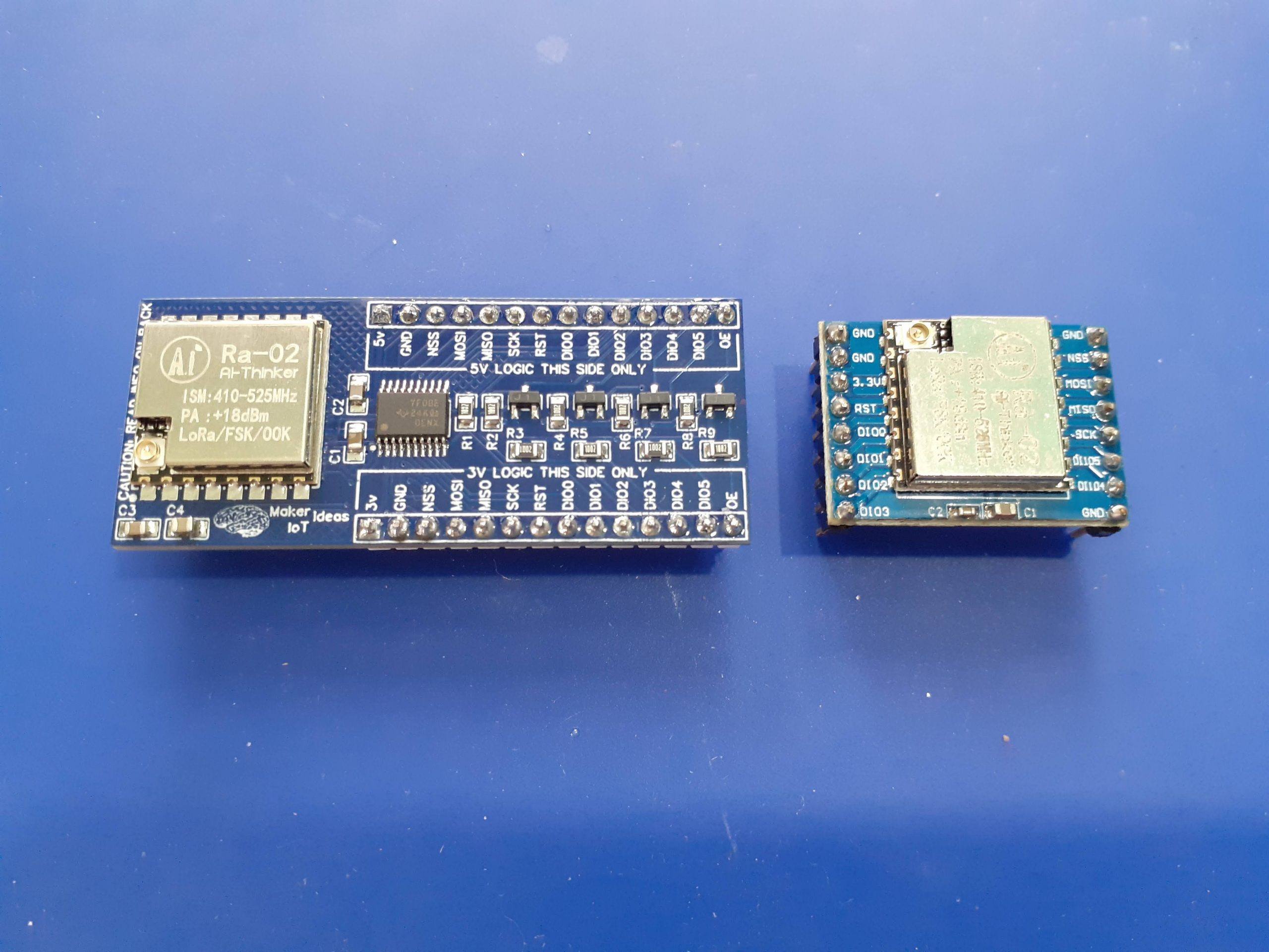
Most Makers and electronics enthusiasts may already know of the RA-02 LoRa Module. Many of them might own an RA-02 Breakout module or two… For those who do, they will surely know about the problems encountered with using this particular breakout module…
The RA-02 module, in itself, is a great piece of kit, and when used on a custom PCB, which was designed with all the little secrets of this module taken into consideration, is a pleasure. Using the RA-02 breakout module, in its existing form factor, does however present quite a few unique challenges, which, if you are unaware of them, can cause quite a few frustrating moments, or even result in permanent damage to the module…
1) The module is based on the SX1278 chip from Semtech and is a 3v device. The IO pins are NOT 5v compatible but seem to work for a few hours or so when used with 5v… This causes many people, especially on Youtube, to assume that it is ok to send 5v logic signals to this module…
I have still not seen any Youtube video telling viewers to at least use a resister divider or logic converter… People just don’t know, and those that know seem to be keeping quiet!
Adding logic converters is in fact specified by the datasheet.
2) Adding logic converters means adding additional wiring, and for a breadboard based project, that adds to the complexity.
3) You have a total of 4 ground pins that need to be connected. not connecting all of them, causes funny things to happen, from overheating down to failure… ( My personal experience while researching this project)
4) The existing breakout module is not breadboarding compatible, resulting in a floating assembly with wires going everywhere, which results in unstable connections etc…
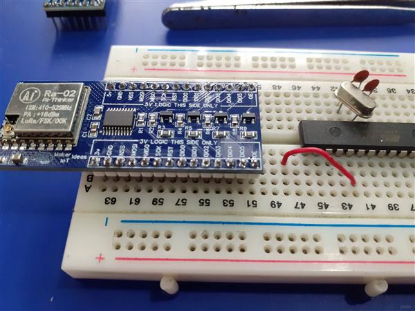
Basically something similar to the picture below:
In this picture, I have an existing RA-02 Breakout Module, with an 8 channel Logic converter and an Arduino Uno clone, along with all the needed wiring to make this setup possible… Quite a lot of wires indeed…
My solution:
I design and use quite a few LoRa PCBs and on all of them, I implement logic conversion using the BSS138 N-MOS Mosfet and 10k resistors. It is a cheap and reliable solution, but it can take up quite a lot of space on a PCB, as this means 11 Mosfets and 22 10k resistors if I were to provide level conversion to all of the RA-02’s GPIO and IO pins…
I also have the constant problem of many unnecessary wires, many of which sometimes fail straight out of the box, when prototyping something. I partly solved that by designing a few dedicated PCB solutions, but that is not always ideal,
Using a dedicated Logic Converter IC, and Mosfet based converters to make up the difference, on a breadboard compatible module, seemed like a good idea, so I went ahead and designed the following solution:
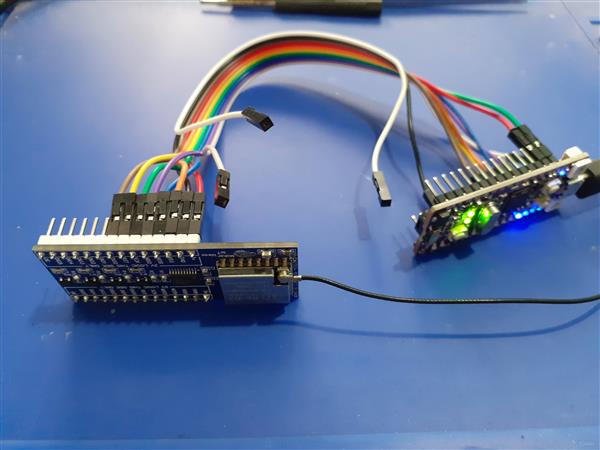
The breakout board module is breadboard compatible, and also has clearly marked pins to indicate the 3v and 5v sides of the module.
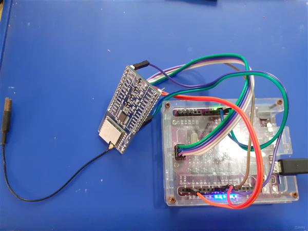
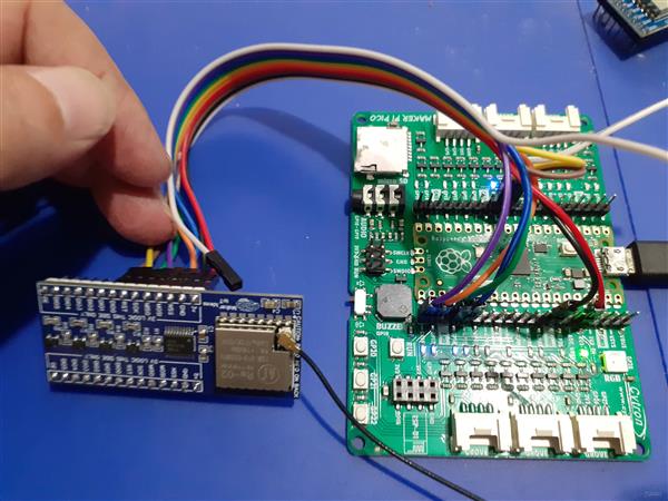
For my first test, I decided to test with an Arduino Uno Clone, since that is what most Makers and students will have access to. I used Cytron’s Maker Uno platform, which is equipped with some added goodies, in the form of diagnostic LED etc to make prototyping a lot easier.
As we can clearly see, It is only necessary to connect to the 5v logic side of the module, as well as provide 3v and 5v + GND to the module
In this test, I used Sandeep Mistry’s LoRa Library, with the Arduino IDE to do a quick test sketch.
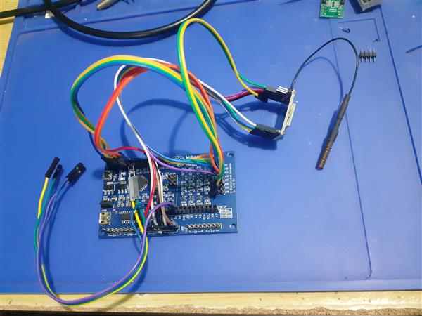
As we can see, you need quite a lot more wires to make this work. It is also worth noting that we have only 8 level converters on this ATMEGA328P PCB, in order to use all of the RA-02’s GPIO, we will need to add an additional external logic converter as well.
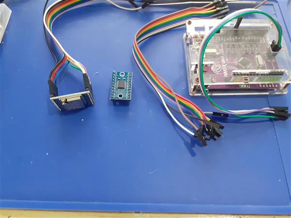
For my second test, I decided to be a bit brave, and try to use the new Raspberry Pi Pico ( RP2040 Microprocessor ). I have quite a few of them lying around and have never really done a lot with them, due to the fact that I do not really like using MicroPython or CircuitPython, and also because the recently released Arduino Core for the RP2040 still being quite new… I decided to use a development board that I recently bought from Cytron, the Maker Nano RP2040, as it has all the added diagnostic features to make my life a bit easier, I will also include a test with an original Pi Pico board, to make it more accessible to everyone out there.
Once again, I used Sandeep Mistry’s LoRa Library, with the exact same Arduino sketch, used for the Maker Uno test. (I obviously needed to change the pin numbers though, as the RP2040 uses different pins for its SPI interface).
Maker Nano RP2040 RA-02 Breakout Module
NSS 17
MOSI 19
MISO 16
SCK 18
RST 9
DIO0 8
In this case, we DO NOT need the OE pin, as the RP2040 is a native 3v device. The level converter can thus stay disabled, with its pins in tri-state ( high impedance ) mode.
If we look at the code, it is similar to the Maker Uno’s code, with only the Pin declarations needing a change
#include <SPI.h> // include libraries
#include <LoRa.h>
const int csPin = 17; // LoRa radio chip select
const int resetPin = 9; // LoRa radio reset
const int irqPin = 8; // change for your board; must be a hardware interrupt pin
byte msgCount = 0; // count of outgoing messages
int interval = 2000; // interval between sends
long lastSendTime = 0; // time of last packet send
// Note that SPI has different names on the RP2040, and it has 2 SPI ports. We used port 0
// CIPO (Miso) is on pin 16
// COPI (Mosi) is on pin 19
// SCK is on pin 18
// CE/SS is on pin 17, as already declared above
I did not use a breadboard, in order to make things as easy as possible.
To make things a bit easier, without having to resort to using a breadboard, I decided to do the Original Pi Pico test using the Maker Pi Pico PCB. This PCB is basically a big breakout module, with detailed pin numbers and some diagnostic LEDs, but it also uses a native Pi Pico, soldered directly to the PCB, by means of the castellated holes… So, While technically not being a true standalone Pico, It makes my life easier and was thus used for the test, as I can be sure that the pins are labelled exactly the same as on the original Pico.
The code used for the Maker Nano RP2040 works perfectly, with no changes required.
This post is getting quite long by now, so I have decided not to include my tests of the ESP-12E ( NodeMCU ) or ESP32 development boards here as well… They also function as expected.
In Summary
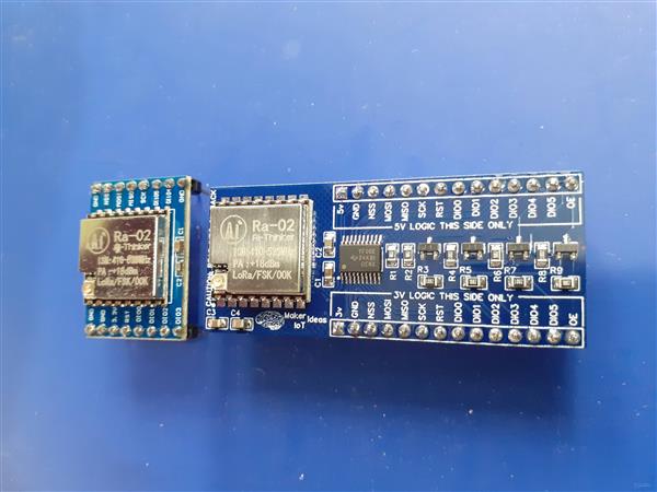
When I started this project, I set out to solve a problem ( personal to me ), that could potentially help a lot of other people use the RA-02 Module for more projects and tasks. The Breakout module in its current form can also be used with the RA-01h module (915Mhz Module) without any changes. All GPIO pins are broken out, and accessible through full logic converted pins on both sides of the breakout module.
I hope that this will be useful to someone. I am also not releasing the full schematics at this stage, as I may decide to make some minor cosmetic changes in the near future.
The PCB can however be ordered from PCBWay in its current form and works 100% as expected. The BOM file is available with the ordered PCB as usual.
This PCB was manufactured at PCBWAY. The Gerber files and BOM, as well as all the schematics, will soon be available as a shared project on their website. If you would like to have PCBWAY manufacture one of your own, designs, or even this particular PCB, you need to do the following… 1) Click on this link 2) Create an account if you have not already got one of your own. If you use the link above, you will also instantly receive a $5USD coupon, which you can use on your first or any other order later. (Disclaimer: I will earn a small referral fee from PCBWay. This referral fee will not affect the cost of your order, nor will you pay any part thereof.) 3) Once you have gone to their website, and created an account, or login with your existing account,
4) Click on PCB Instant Quote
5) If you do not have any very special requirements for your PCB, click on Quick-order PCB
6) Click on Add Gerber File, and select your Gerber file(s) from your computer. Most of your PCB details will now be automatically selected, leaving you to only select the solder mask and silk-screen colour, as well as to remove the order number or not. You can of course fine-tune everything exactly as you want as well.
7) You can also select whether you want an SMD stencil, or have the board assembled after manufacturing. Please note that the assembly service, as well as the cost of your components, ARE NOT included in the initial quoted price. ( The quote will update depending on what options you select ).
8) When you are happy with the options that you have selected, you can click on the Save to Cart Button. From here on, you can go to the top of the screen, click on Cart, make any payment(s) or use any coupons that you have in your account.
Then just sit back and wait for your new PCB to be delivered to your door via the shipping company that you have selected during checkout.