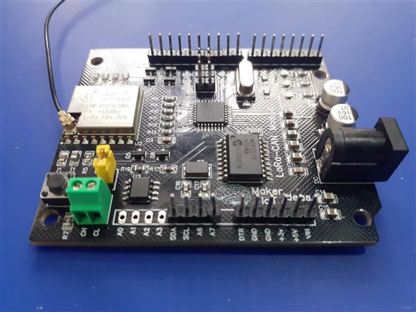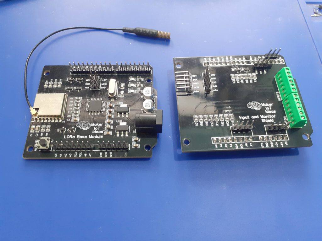

CAN-Bus allows us to add a lot of devices to a single bus (theoretically up to 127, with a practical limit of about 110). It was logical to decide to use CAN-BUS for communication between my LoRa-CAN Module and remote nodes in my ongoing farm telemetry system. In a previous project, I introduced the LoRa-CAN Gateway, which will be used to send/receive messages from the master control unit, the SX127x-RA-02-Module.
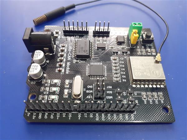
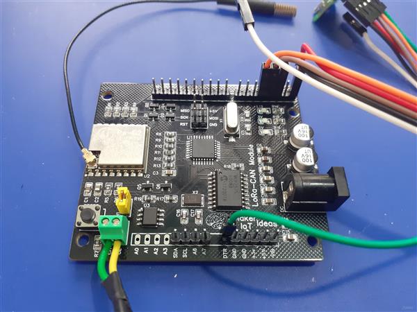
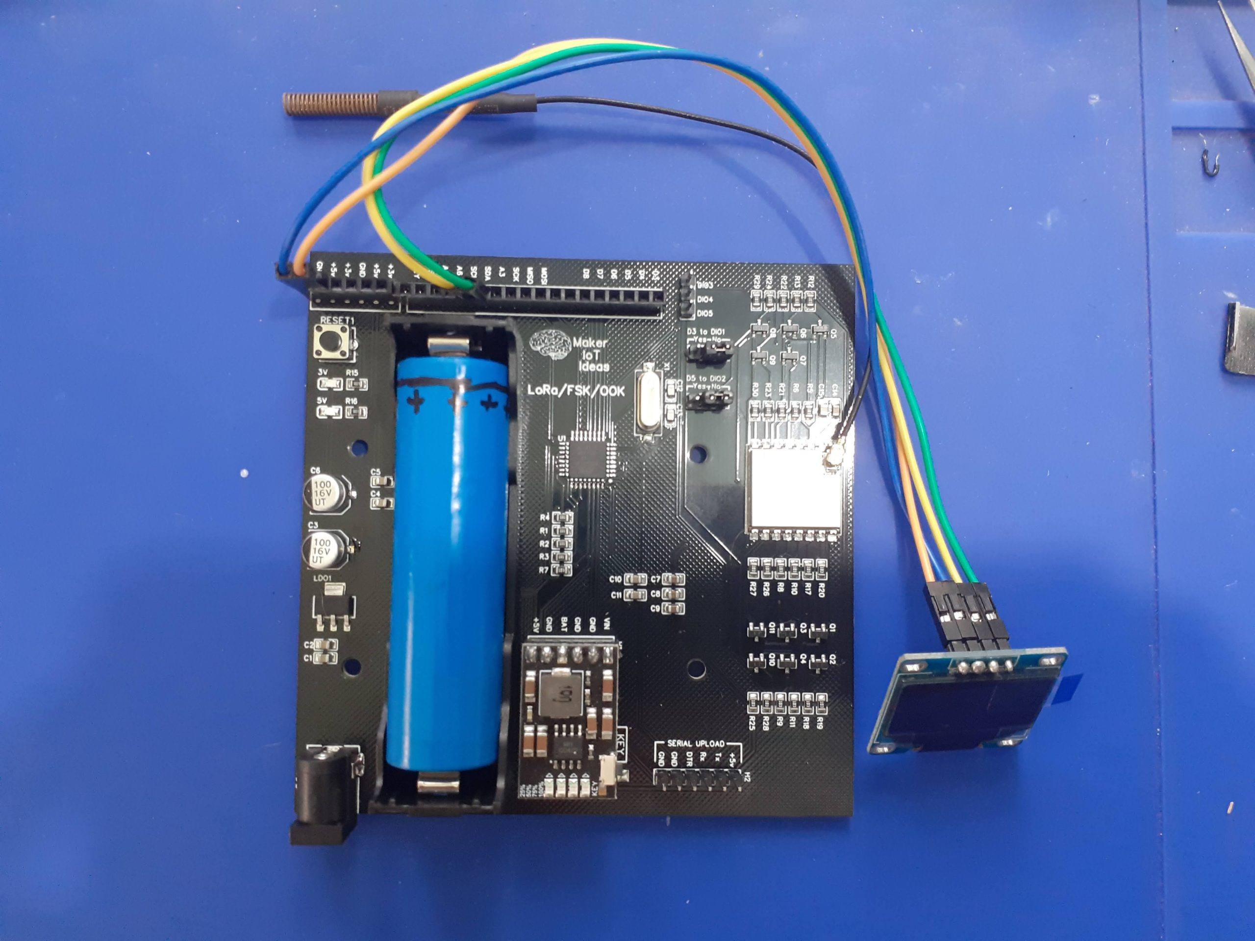
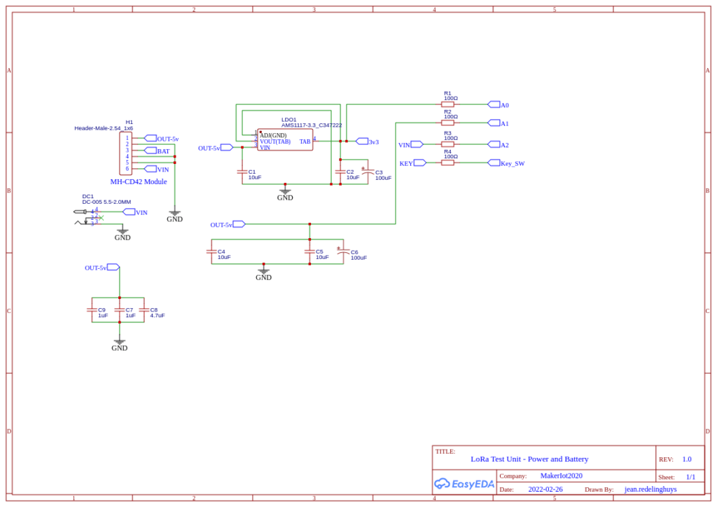
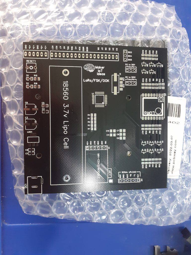
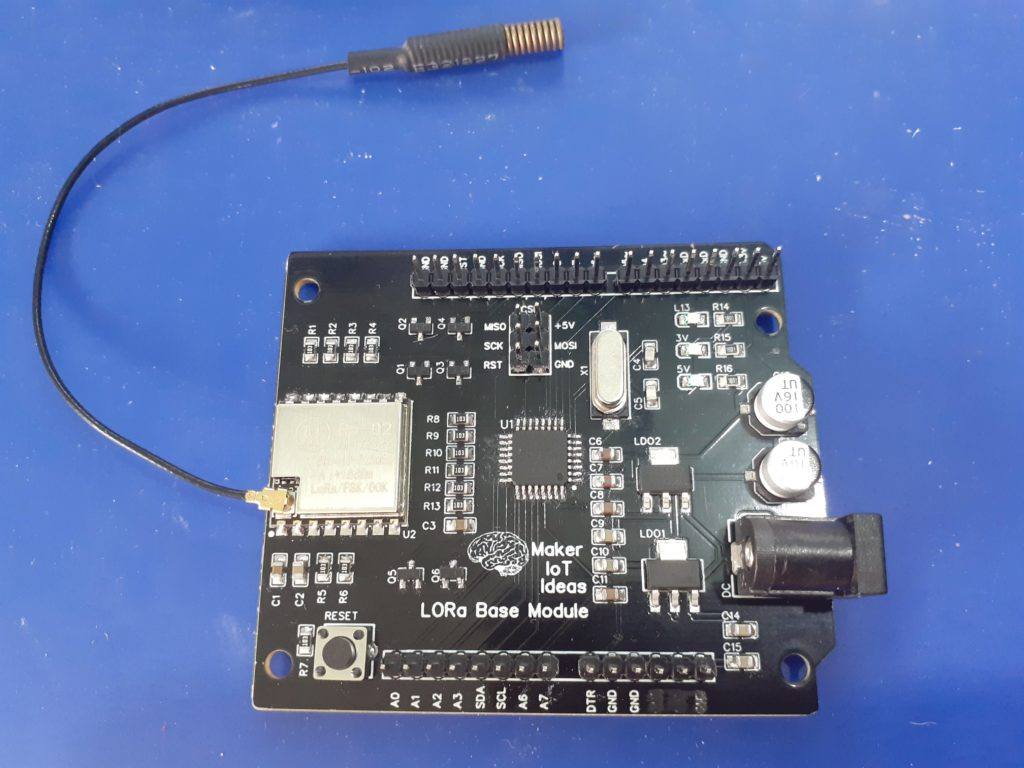
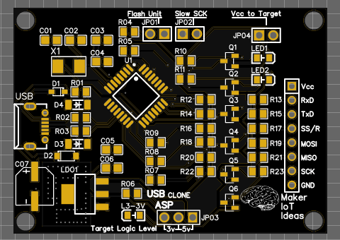
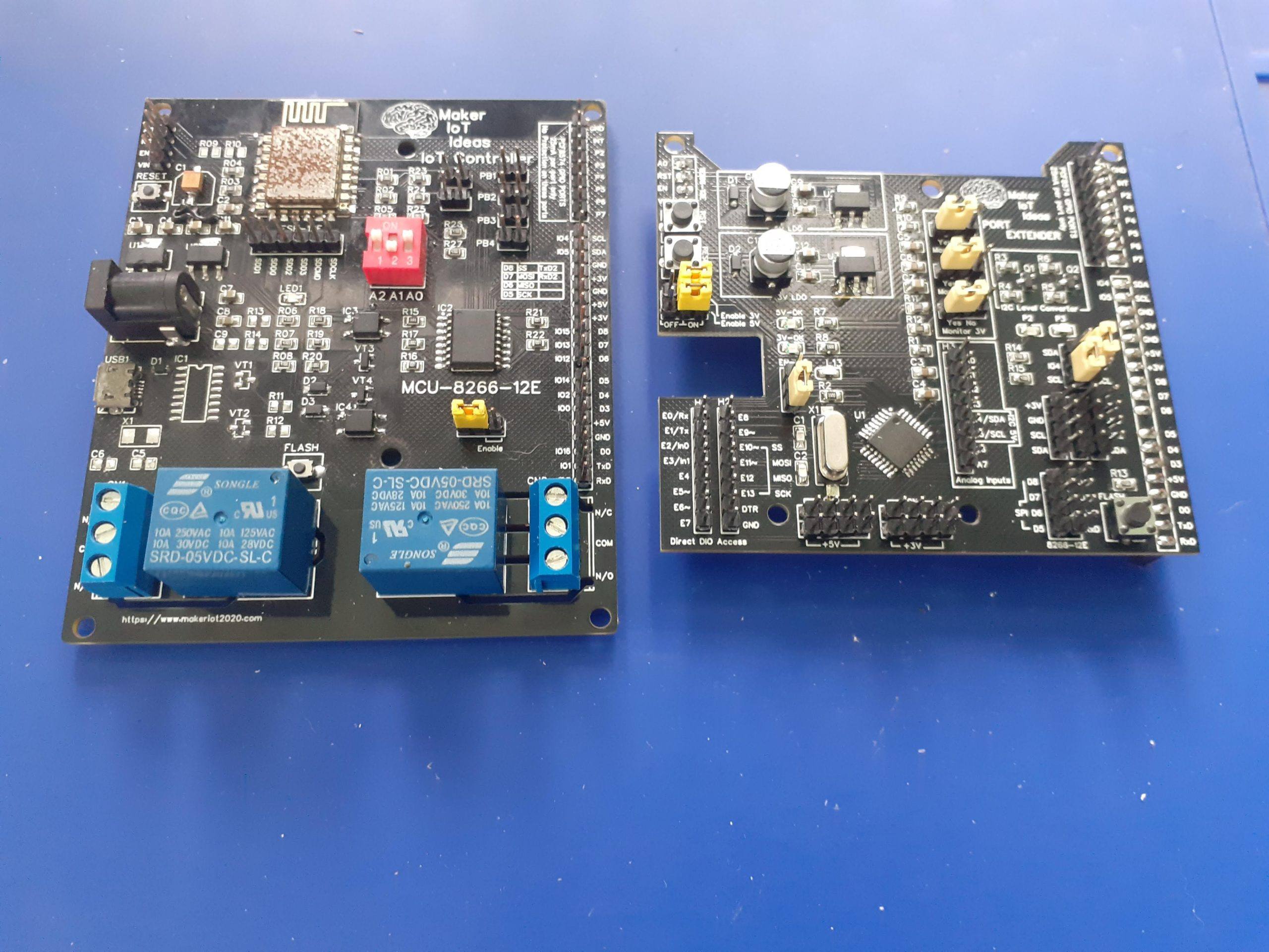
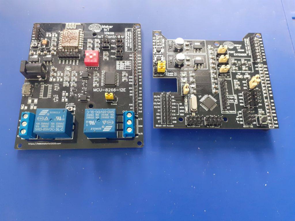
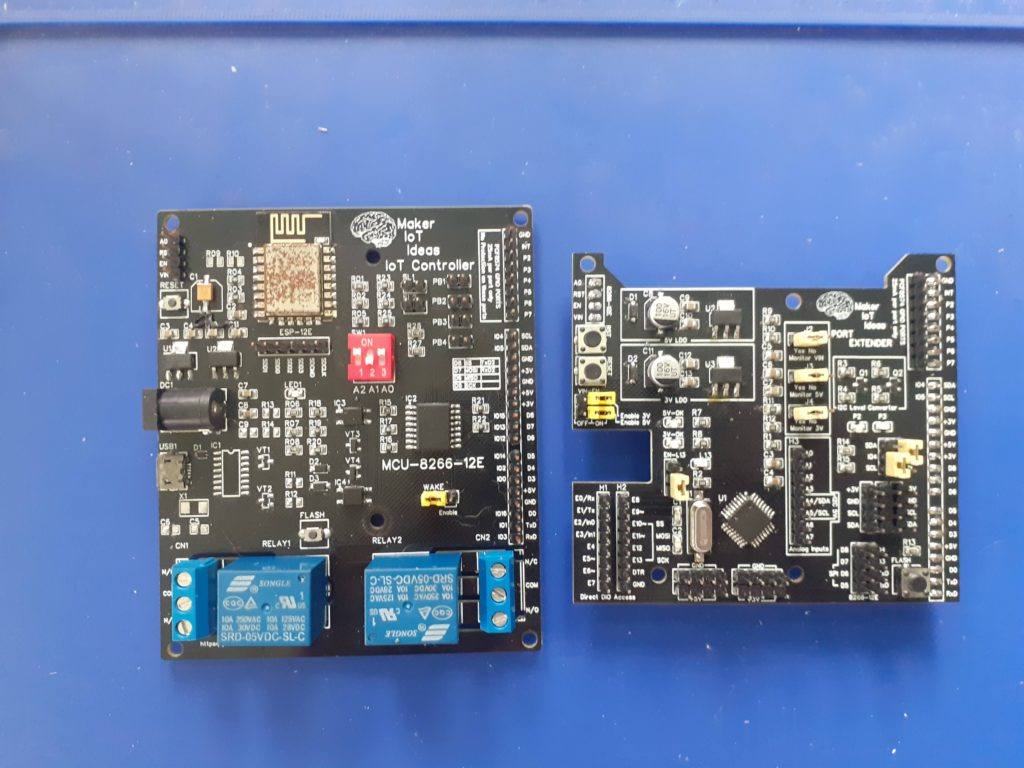
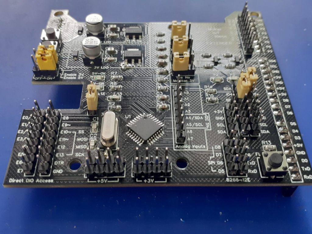
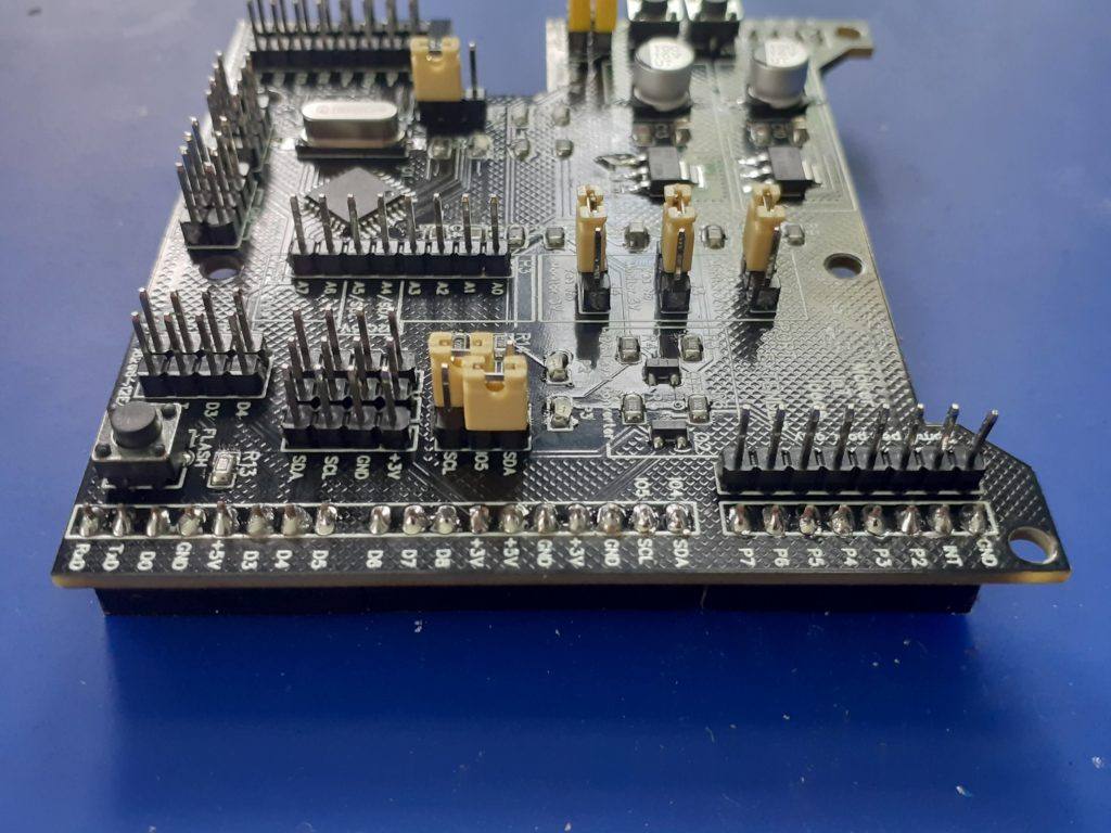
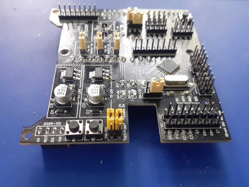
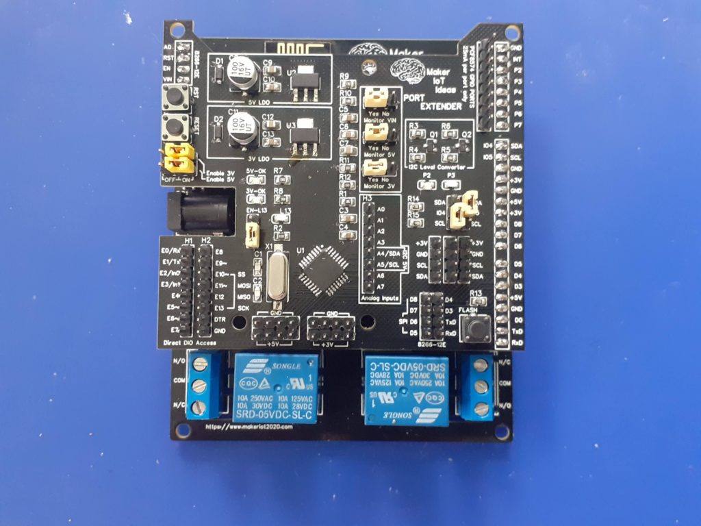
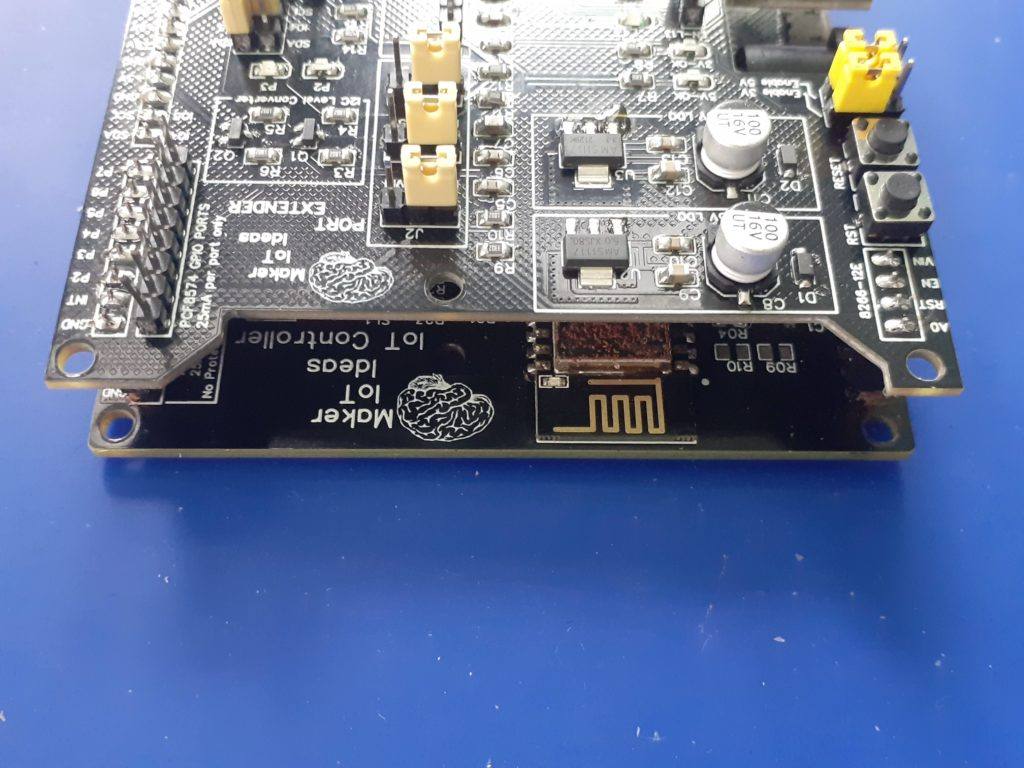
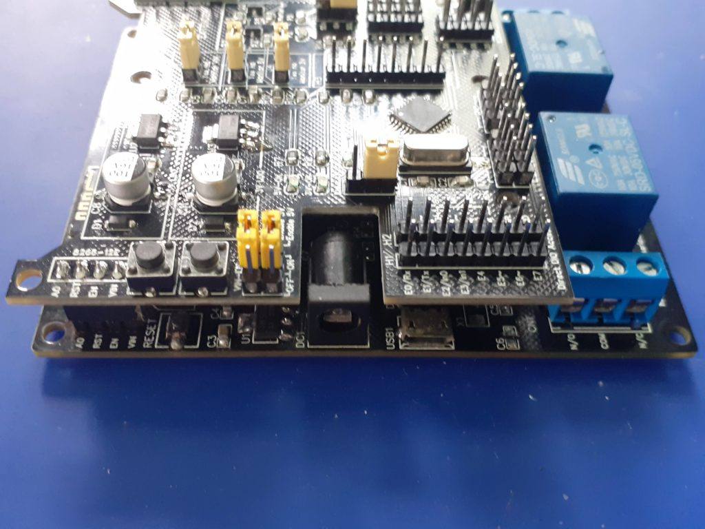
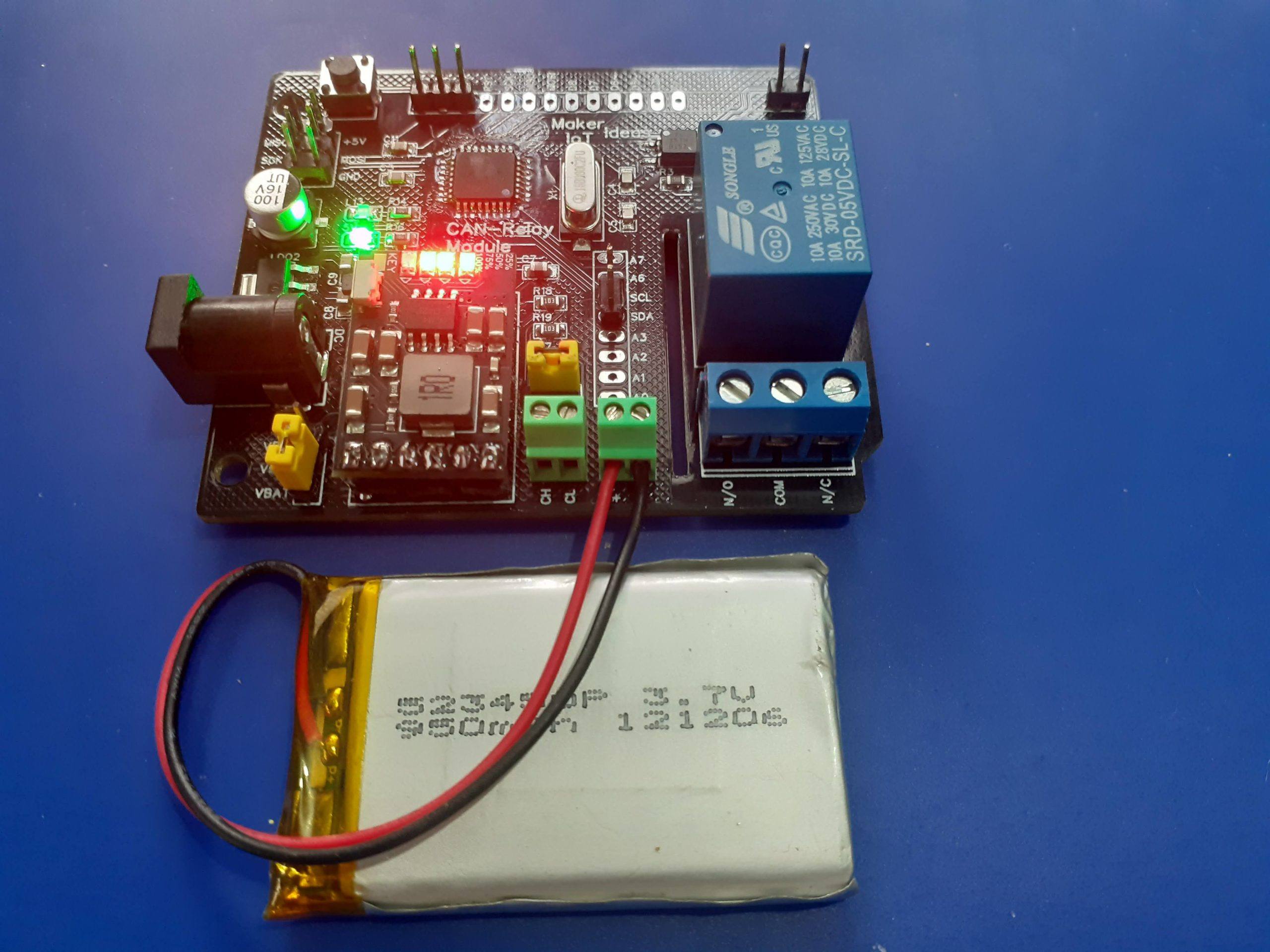
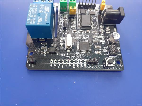
Today, I will focus on the design of the node device, an Arduino compatible CAN Relay Module PCB, with a built-in, CAN Controller and Transceiver ( MCP2515 and TJA1050 ), and the option to be powered from a LiPo battery (18650 or Single 3.7v Lipo cell), with charging provided by an MH-CD42 Module, similar to that used in the SX128x project mentioned above. The Module can also be powered directly from up to 12v DC by placing Jumper H2 in the V-REG position…
As mentioned in a previous project, the MH-CD42 module can provide up to 2A of current to charge a battery and provide 5V DC on a direct bypass circuit to power the rest of the circuit while the battery is being charged. This feature makes it ideal for my intended use, as I would only be needing battery power at night when the off-grid solar powered inverter is not actively charging the main batteries, and providing 220v AC.
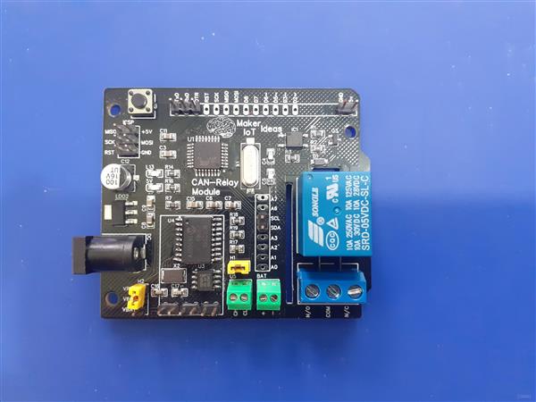
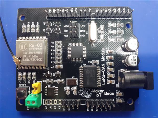
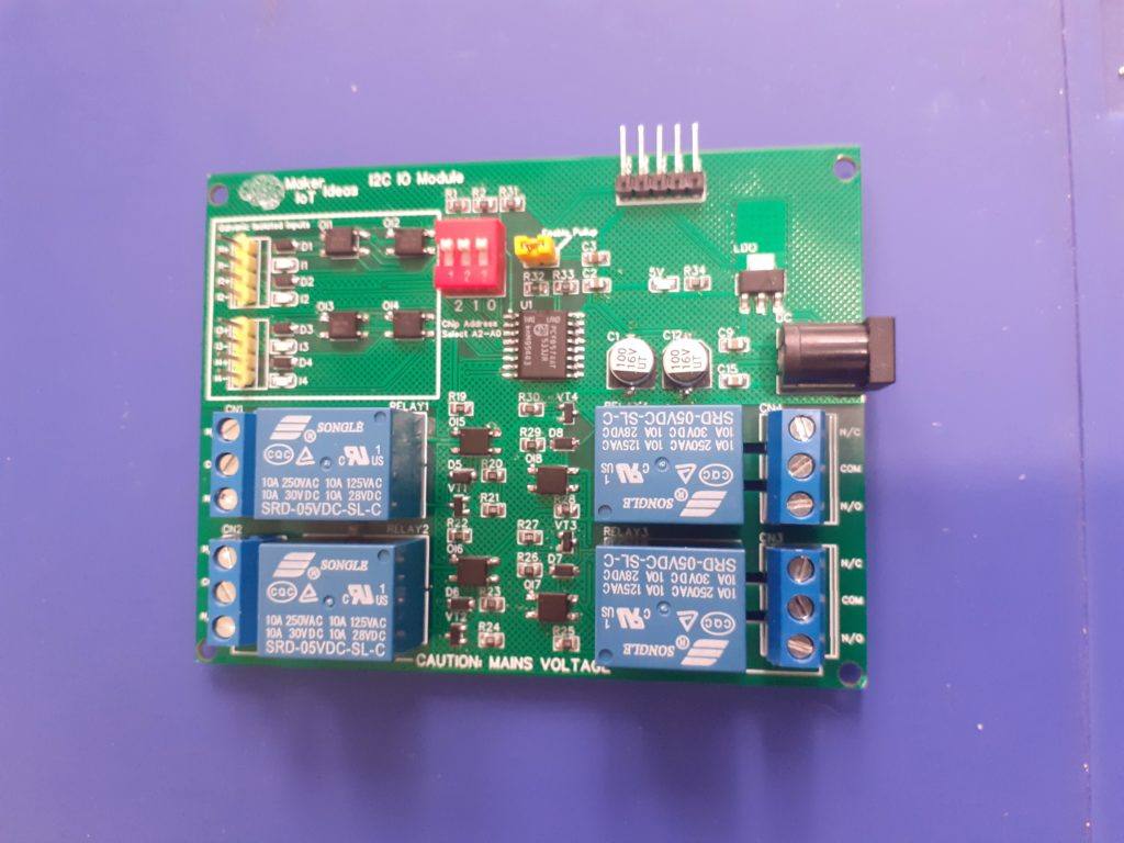
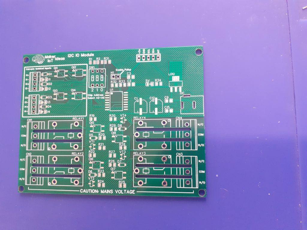
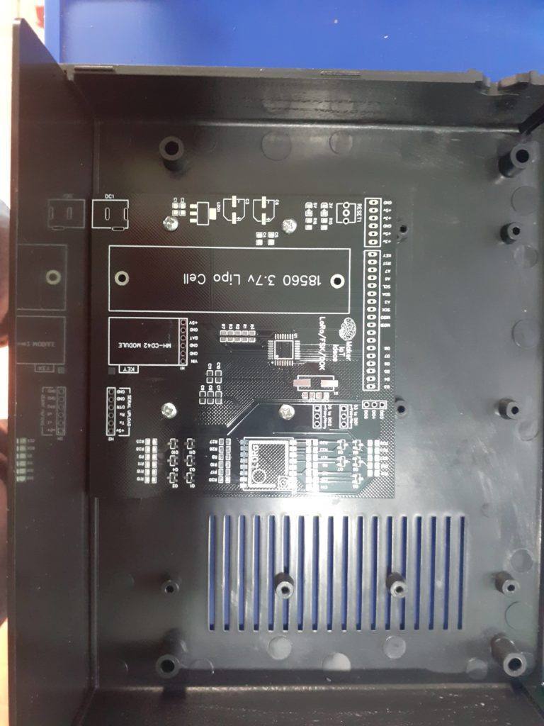
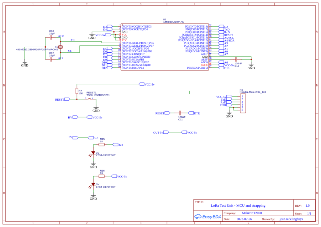
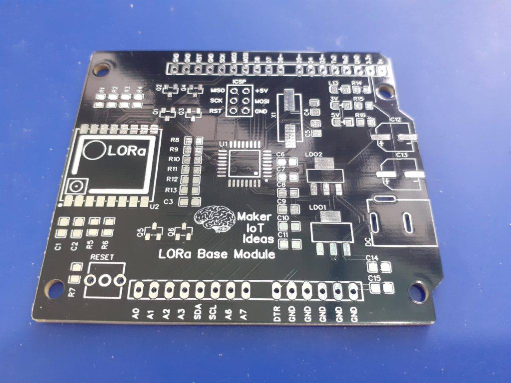
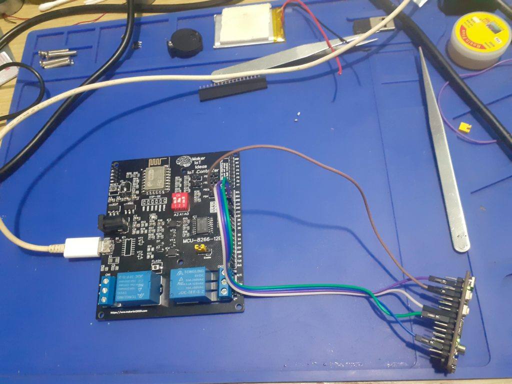
The CAN Relay Module PCB was designed to be as compact as possible, with a total footprint of the standard Arduino UNO. As space was at a premium, and to ensure that there are the absolute minimum additional components that will consume power when operating from the battery, I have not included any USB-to-Serial converters onboard. Firmware can be uploaded with an AVRASp, USBASP, Arduino as ISP or even an external USB-to-Serial converter ( providing that you load a bootloader into the Atmega Chip).
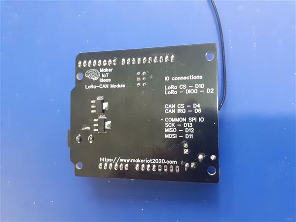
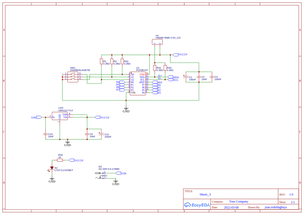
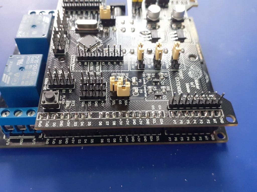
All of the unused GPIO pins on the ATMEGA chip is broken out into headers, with the exception of D10 ( which is used as CE/SS on the MCP2515 CAN controller), D9 which is connected to the Interrupt from the MCP2515, and D4, which is used to control the onboard Relay.
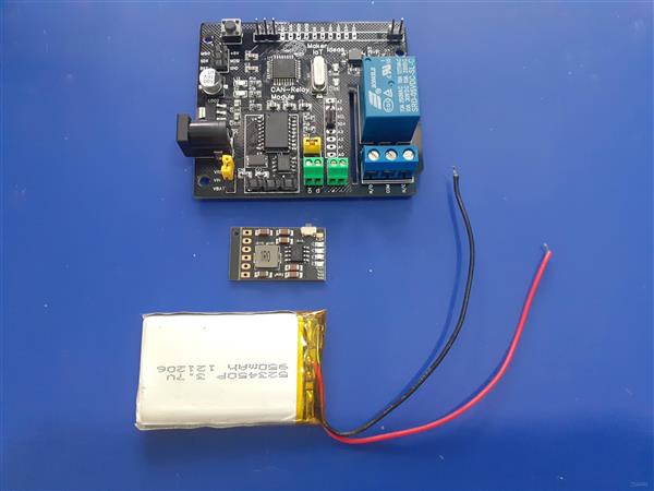
The MH-CD42 Module, and LiPo or 18650 Battery are completely optional, The device can function without these, by moving the H2 jumper to the VREG position as already mentioned above. This will divert the DC Voltage(Up to 12v) from the DC input adapter to the build-in 5v LDO voltage regulator to power the device.
If you place the H2 Jumper in the VBAT position, you need to install the MH-CD42 module to provide power to the rest of the PCB, as well as keep the LiPo battery or 18650 Cell charged…
Please NOTE:
When the MH-CD42 module is in use, the total DC input voltage through the DC input adapter SHOULD NOT exceed 5.5v DC! This is a limitation in the operating parameters of the MH-CD42 module. Not paying attention to this will result in damage to the MH-CD42 Module.
You could also power the module with REGULATED 5v DC, directly from any 5v header pin. Please note that in this case,
1) The battery won’t be charged.
2) The LDO regulator will not be in operation.
The Microcontroller
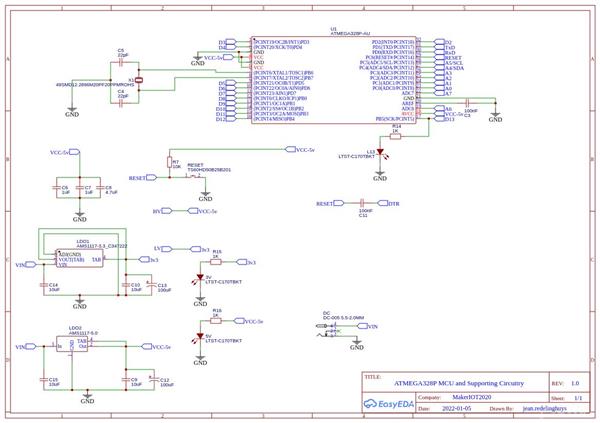
The CAN Relay Module can use any of the ATMEGA8a/88/168/328 AVR microcontrollers, as the pinout is identical. I believe this is an advantage, especially with the current chip prices, where my last quote for an ATMEGA328P-AU was 69$USD!!!! This is in comparison to the 4 to 5 USD each for an ATMEGA8a or ATMEGA168 ( We must also remember though that the 328p is very well known, and thus have higher demand. The 8a/88 or 168 are less well known, have much less memory and flash area, and will thus be cheaper. A word of action though, I had strange issues with I2C on the Atmega8a with Mini core, to such an extent that I2C does not work at all?
If you plan to use I2C on this board, install a 328p right from the start, and save yourself a lot of headaches!
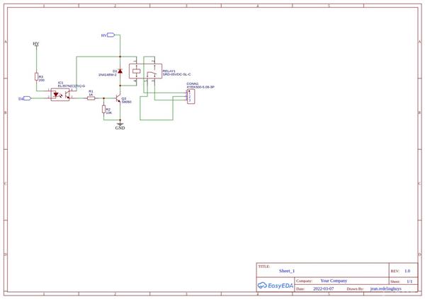
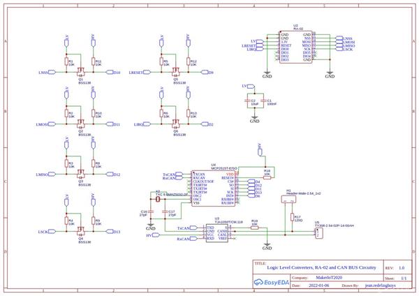
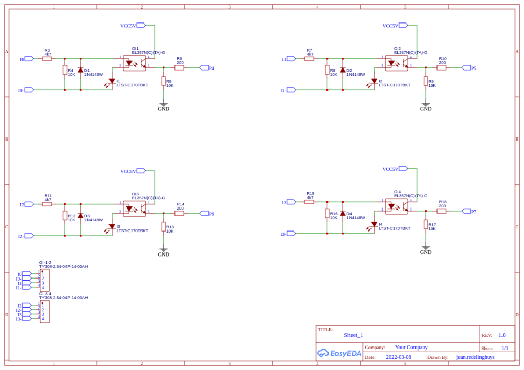
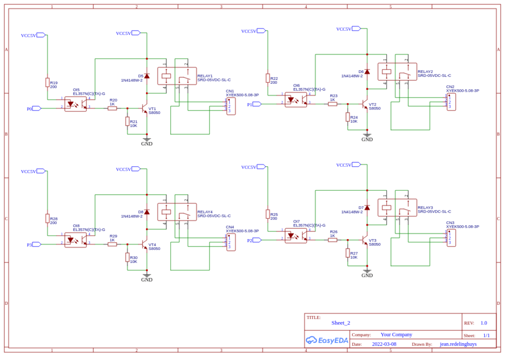
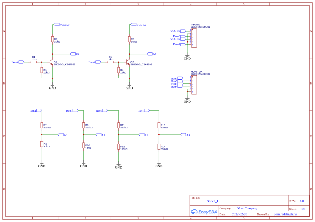
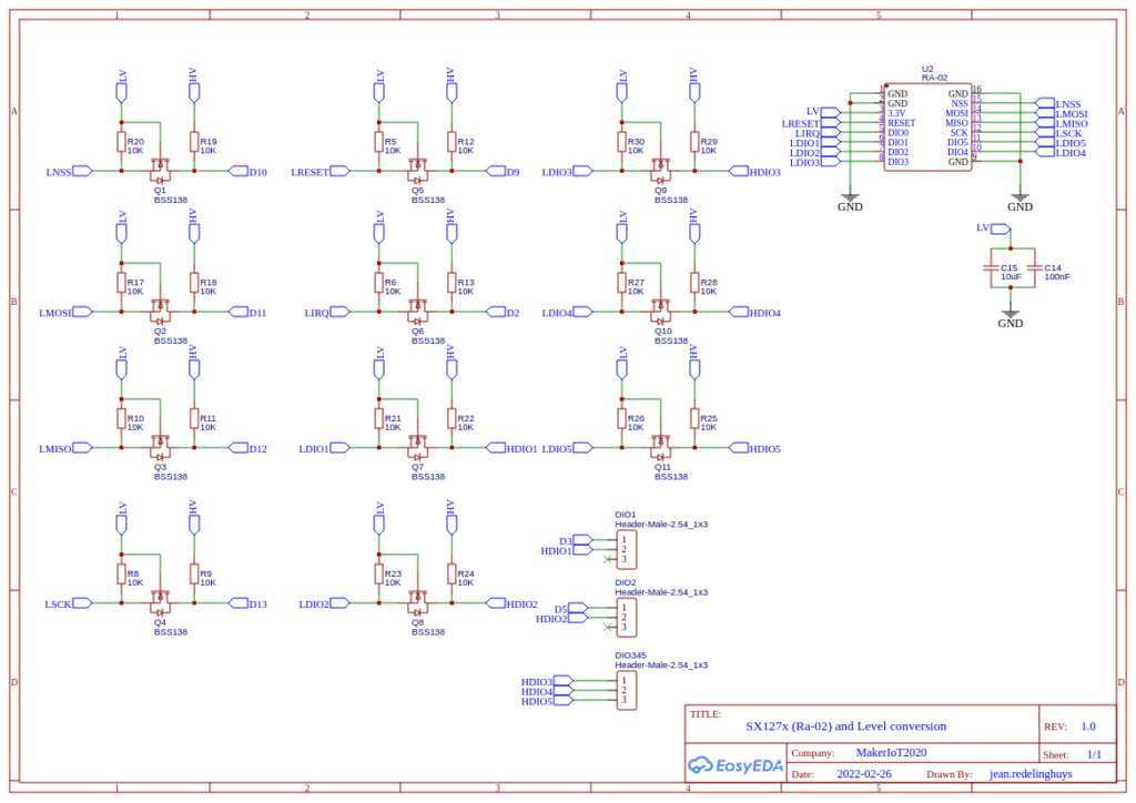
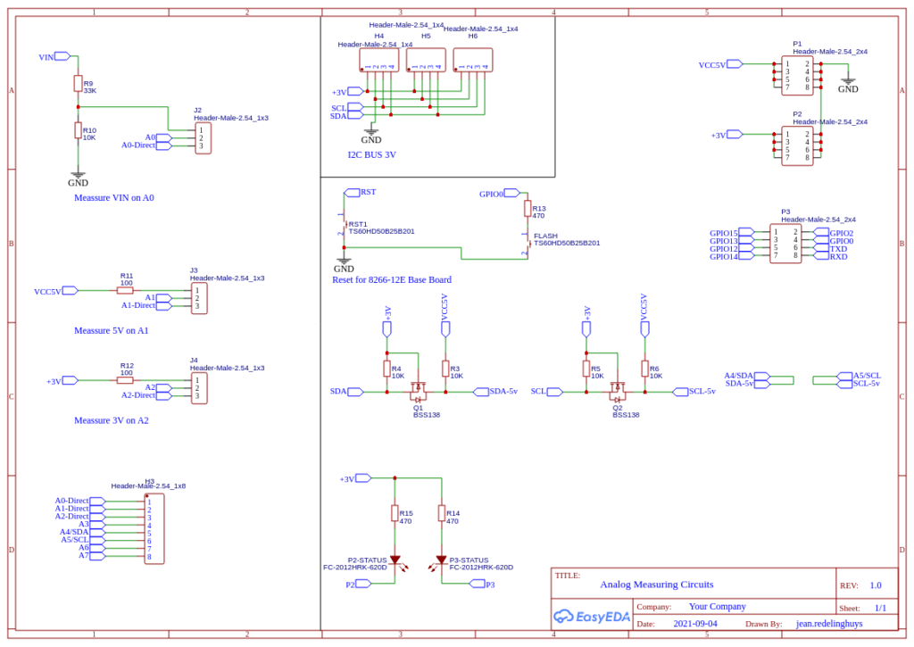
This is the Relay driver circuit. As you can see, it is optically isolated, and active LOW. This means that you have to pull D4 LOW to energise the relay. Also note that, although the relay is optically isolated from the microcontroller, the coil is NOT galvanically ISOLATED. The load, which is magnetically switched, will be truly galvanically isolated, providing of course that you don’t do something silly like using a common ground to the PCB as a common on the relay…
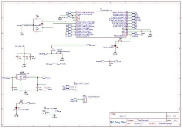
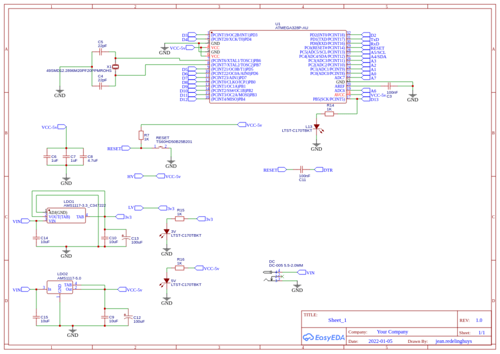
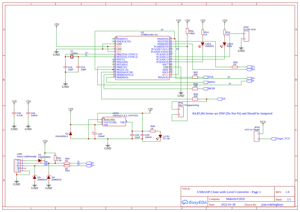
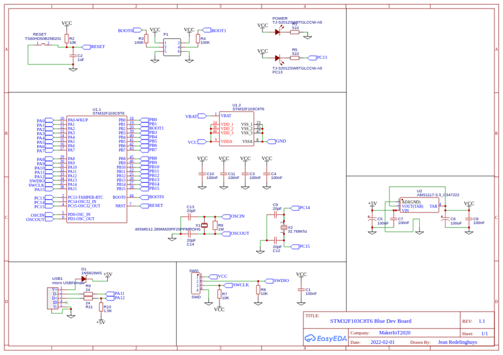
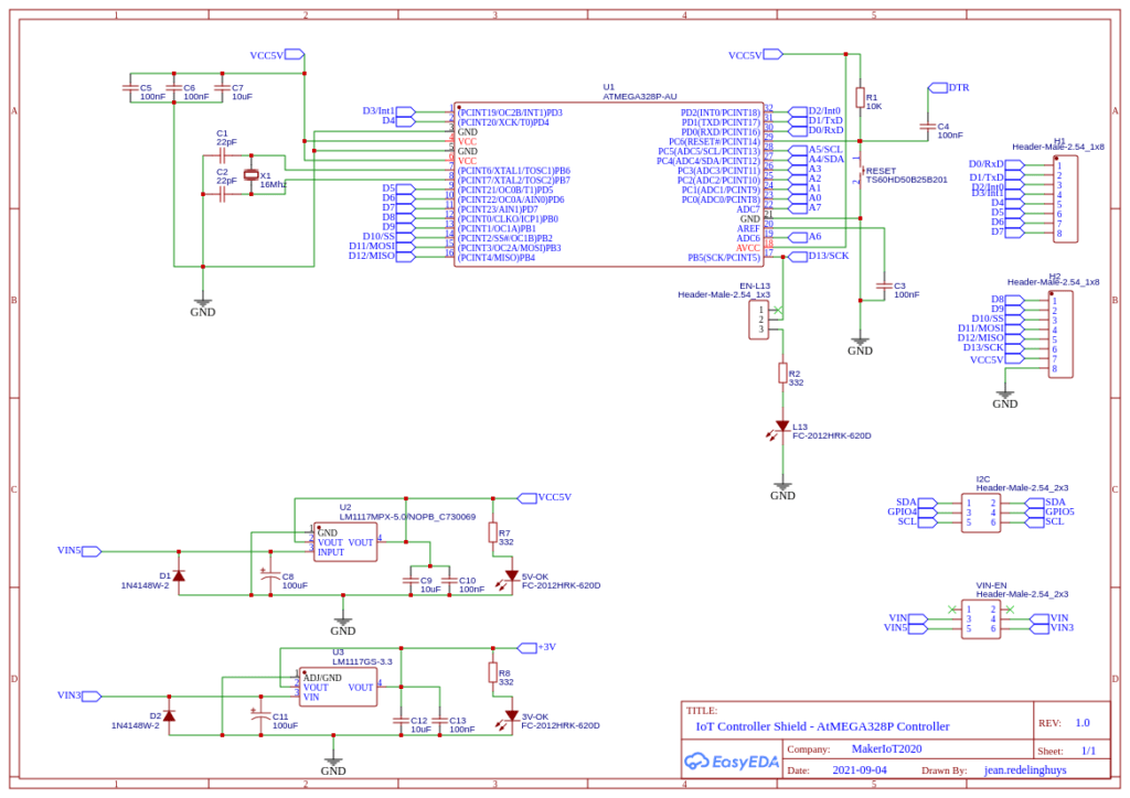
This is the Processor and Power-supply schematic. The circuit is basically a standard Arduino Nano, with modifications for the CAN Controller on the next schematic page. Note that the MH-CD42 is not shown on the schematic. The VBAT net connects directly to the VIN pin on the unit, with the BAT net connecting to the positive of the battery. VOUt-5v from the module goes directly to the 5v net. All grounds are commoned.
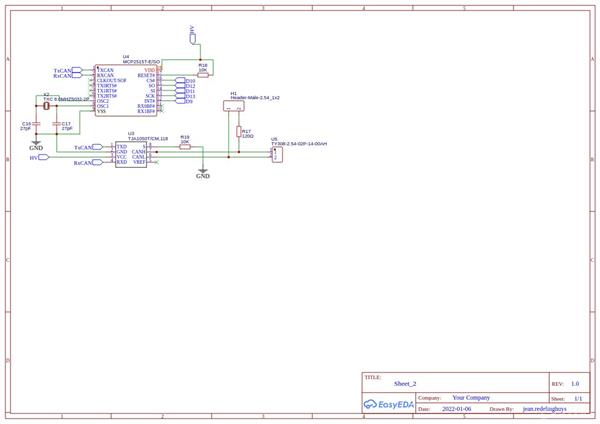
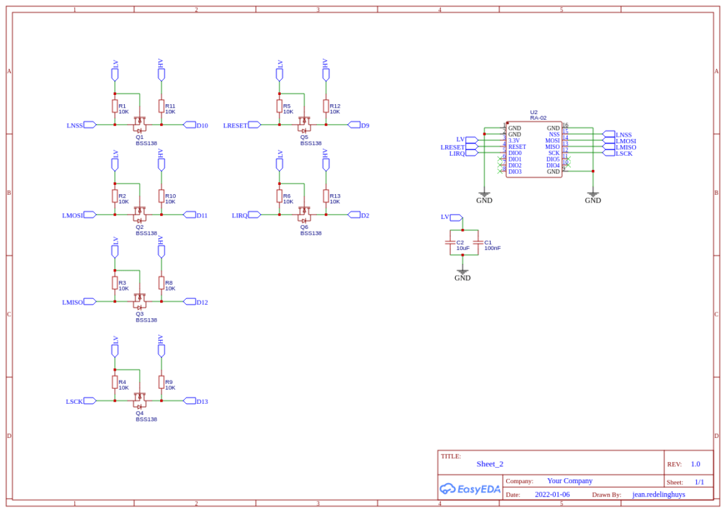
This is the CAN Controller and Transceiver circuitry. The MCP2515 connects directly to the SPI bus on the microcontroller via D13, D12 and D11, with D10 as CE/SS and D9 as Interrupt or IRQ. It is important to note that although the MCP2515 is a 3v capable device, the TJA1050 Can transceiver is 5v only. This prevents us from running the PCB at 3v unless, of course, we change the TJA1050 out for a 3v capable device…
CODE
The board has been extensively tested with Cory J Fowler’s mcp_can Arduino Library. It works very well indeed.
As I am currently working on the final integration of the two modules, I am not yet ready to publish my final code, showing the operation between the CAN-Bus and LoRa-to-CAN Gateway device in this post. Once I am happy that all issues are definitively sorted out, I will publish my code.

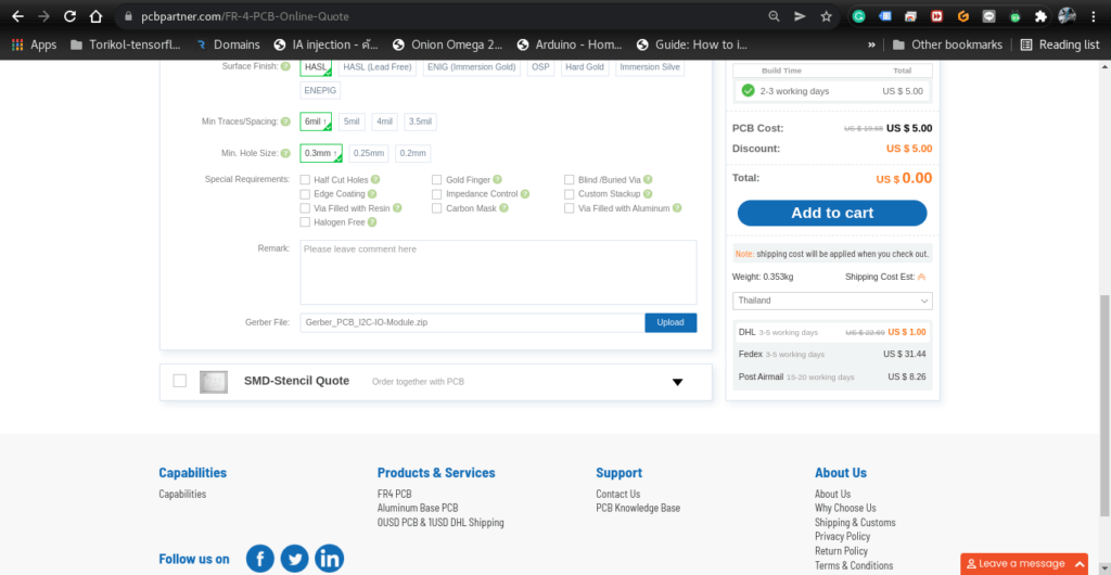
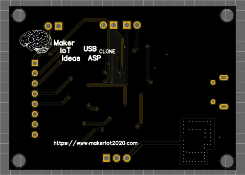
This PCB was manufactured at PCBWAY. The Gerber files and BOM, as well as all the schematics, will soon be available as a shared project on their website. If you would like to have PCBWAY manufacture one of your own, designs, or even this particular PCB, you need to do the following…
1) Click on this link
2) Create an account if you have not already got one of your own.
If you use the link above, you will also instantly receive a $5USD coupon, which you can use on your first or any other order later. (Disclaimer: I will earn a small referral fee from PCBWay. This referral fee will not affect the cost of your order, nor will you pay any part thereof.)
3) Once you have gone to their website, and created an account, or login with your existing account,
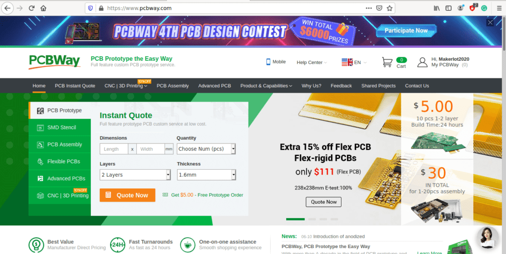
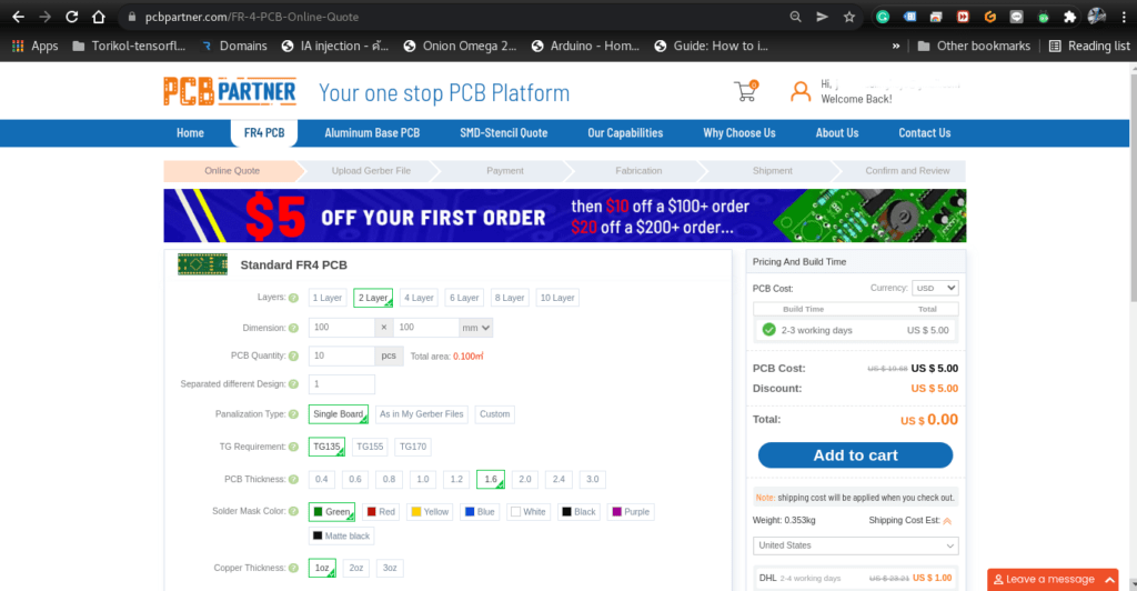
4) Click on PCB Instant Quote
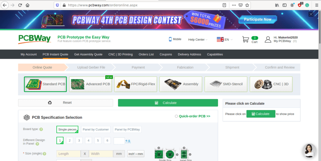
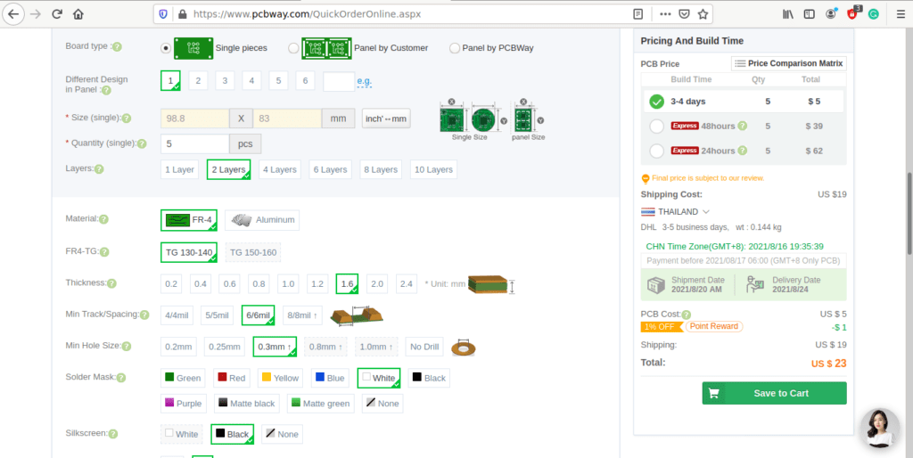
5) If you do not have any very special requirements for your PCB, click on Quick-order PCB
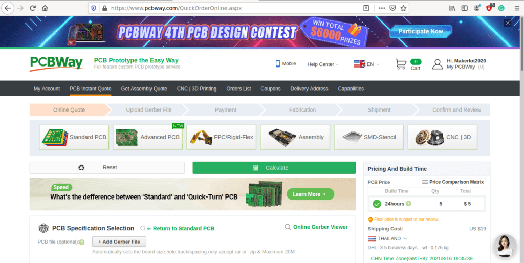
6) Click on Add Gerber File, and select your Gerber file(s) from your computer. Most of your PCB details will now be automatically selected, leaving you to only select the solder mask and silk-screen colour, as well as to remove the order number or not. You can of course fine-tune everything exactly as you want as well.
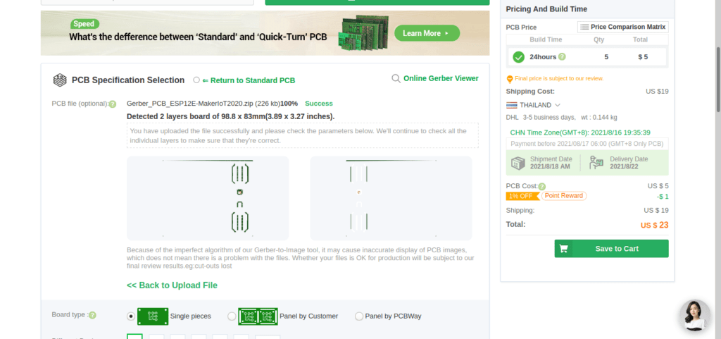
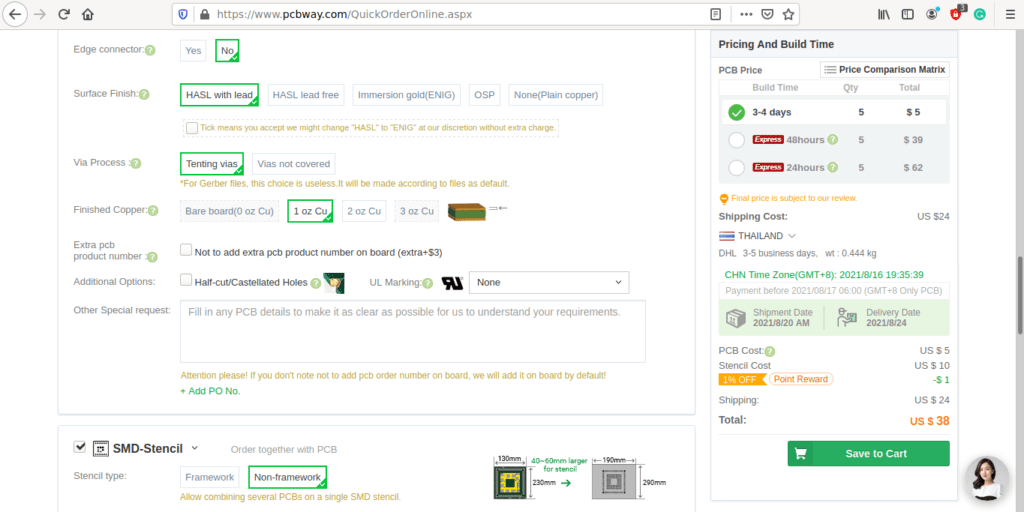
7) You can also select whether you want an SMD stencil, or have the board assembled after manufacturing. Please note that the assembly service, as well as the cost of your components, ARE NOT included in the initial quoted price. ( The quote will update depending on what options you select ).
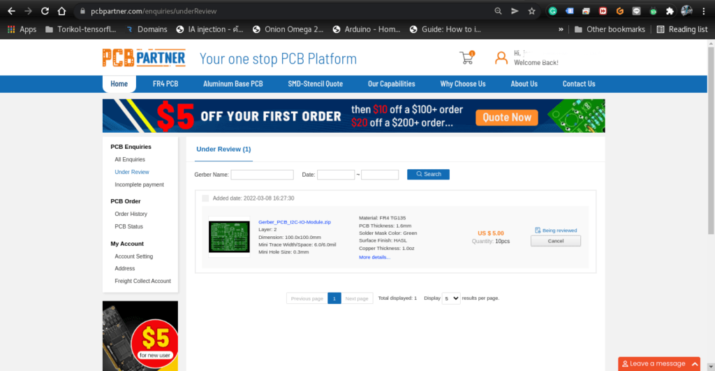
8) When you are happy with the options that you have selected, you can click on the Save to Cart Button. From here on, you can go to the top of the screen, click on Cart, make any payment(s) or use any coupons that you have in your account.
Then just sit back and wait for your new PCB to be delivered to your door via the shipping company that you have selected during checkout.