Most of us are familiar with voice assistants these days; Google Assistant, Siri and Alexa are obviously the most well-known of these. They all share a common problem though: They are online, and can thus secretly record everything you say around them, for later use by their respective owners [ The Companies that created them ]. Having a true offline voice assistant can thus seem like the holy grail for privacy and security-minded people.
Introducing VC-01/VC-02

I was recently contacted by AI-Thinker and asked if I was interested to play with a new product of theirs, an offline voice module. I immediately jumped at the opportunity, as this was something that I wanted to get my hands on for a long time, providing it works of course…
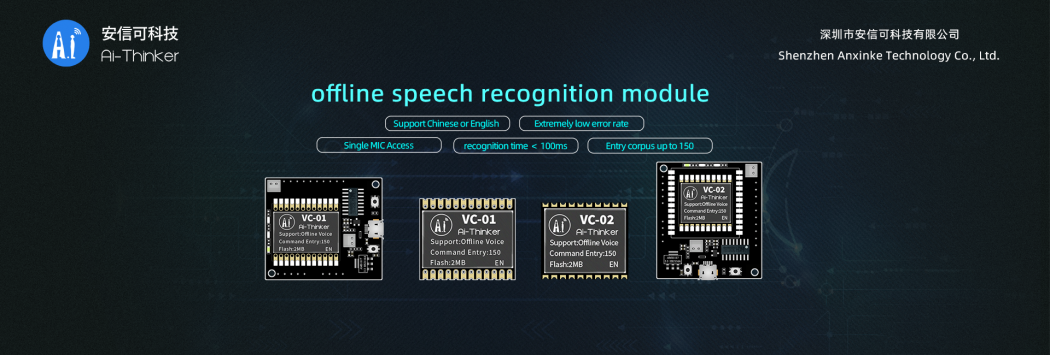
AI-Thinker’s offline voice module is available in two models, the VC-01 and the VC-02.
My Sales Representative (Kat ) sent me both models, in a kit format, complete with speaker and microphone. The kit PCB also provides a USB port with a ch340 chip, as well as two push buttons (reset and wake-up) as well as 3 built-in LEDs ( White, Orange and Blue ).
These light up with the factory firmware, depending on what commands are issued to the device…
Let us take a look at how the factory firmware works; Thank you to Kat from Ai-Thinker for uploading the video, and sending the link to me 🙂
As we can see in the video above, the module seems to work very well… The question now arises if it can be customised to do what we want it to…
Custom Firmware – Do-able, but with a few caveats
Information in English on this module is very sparse. This is due to it being very new, and with AI-Thinker focusing most of their efforts for this module on the Chinese market for the time being. Which makes sense in one way, but also doesn’t in another.
After spending quite a bit of time trying to get information, my Sales Rep eventually gave me access to an online configuration utility, now be warned:
This is not for the faint of heart. The entire interface is in Chinese ( They are working on an English version, with time-to-completion between one (1) to four(4) weeks from starting the project. I can however not give any accurate dates at this stage, but was told that this development is underway).
Being no stranger to different languages, I thought to use google translate to translate the website. No, that didn’t work. Google refuses or the Chinese Website doesn’t allow it to? No answer as of yet. Any readers who do know any reasons for this, please comment below.
I was sort of successful in manually copy pasting line by line into google translate and got some translation back, but it was not very useful.
My next point to try was asking AI-Thinker to generate some firmware with the web tool. They gladly did that, and that works great. It is however not feasible in the long term to go that route every time.
This was possible because the AI-Thinker engineers, using the firmware development software, currently only available in Chinese, can set custom wake words and train voice commands with a 95% accuracy rate, before generating firmware and flashing it onto the respective module.
Write your own, someone will obviously say, and that was my next attempt. There is an API, and source code on GitHub, as well as Gitee ( The Chinese version of GitHub) The two sources are however not synced, and I was still not successful in getting anything useful from Gitee, once again due to a language issue, as well as the fact that some of the sources depend on 32bit dependencies for Ubuntu, whereas I am running a 64bit version… I did try it though, and can not report any success on that venture at all.
Once again, I will advice us all to wait for AI-Thinker to release an English version of the SDK and API for us all to use, which I am sure they will do at some stage in the near future.
See the video below of my custom firmware, once again demonstrated by Kat from AI-Thinker
As we can see, it once again performs well, with a few issues, but quite acceptable…
Hardware access to the real world
As we have just seen in the video, there is also hardware access via pins, to the real world. There are however a few issues there as well…
Hardware pins are limited.
I2C and SPI, although advertised, are apparently not yet supported in any of the current firmware – Someone with information, please comment…
While there are 2 I2C interfaces, they can not be used at the same time
Information on the module
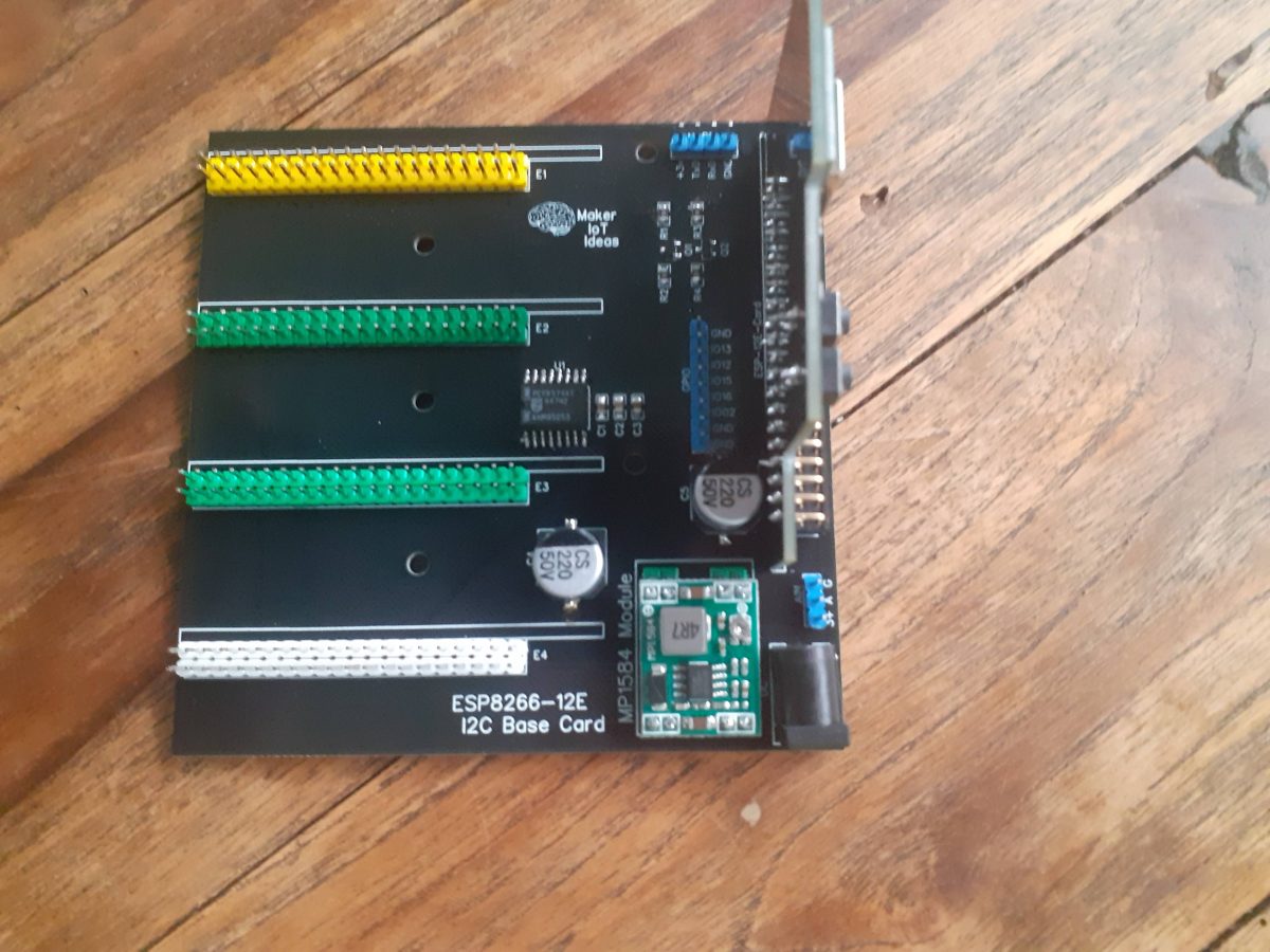
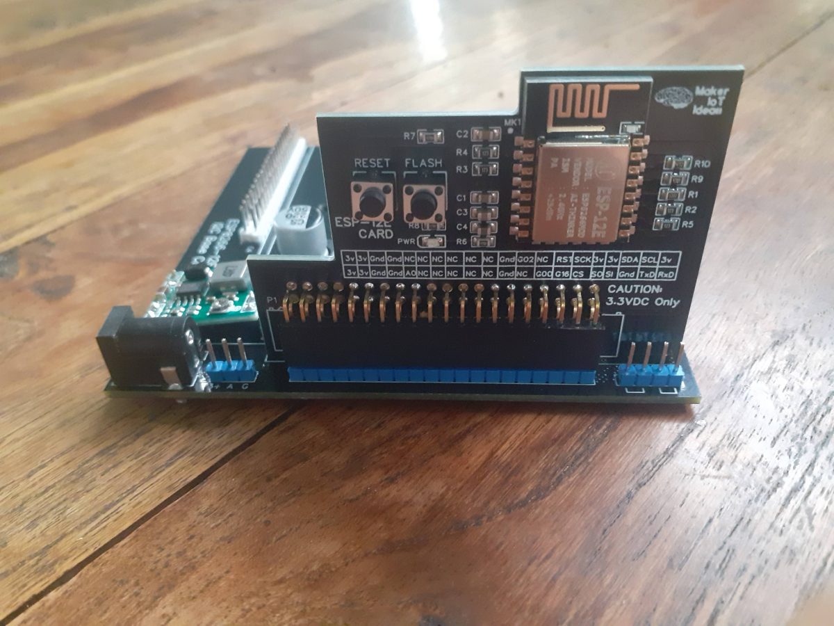
PCB Prototype – Of my own design
As a proof of concept, I have decided to design a quick prototype with relays to use as a more detailed test. I will update information on that soon…
My Conclusion
I definitely see potential here. This is a product which can be quite useful in the future, providing that the following is done:
Proper detailed documentation is provided in English as well as Chinese
API and SDK access is made available in English as well as Chinese
Firmware be updated to make all features available
Having said all of that, I do understand that development, and especially R&D do take a lot of time. Translating documents accurately does too.
I want to congratulate AI-Thinker on producing a very well-made unit, that will definitely bring the dream of a totally offline voice assistant a little bit closer to being a reality.
Voice recognition with my bastard South-African/British English Accent, heavily influenced by Afrikaans, went extremely well, even with the factory firmware.
I do thus not think anybody that can speak passable English will have a problem using the unit.