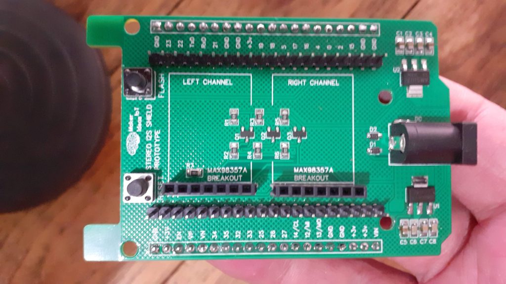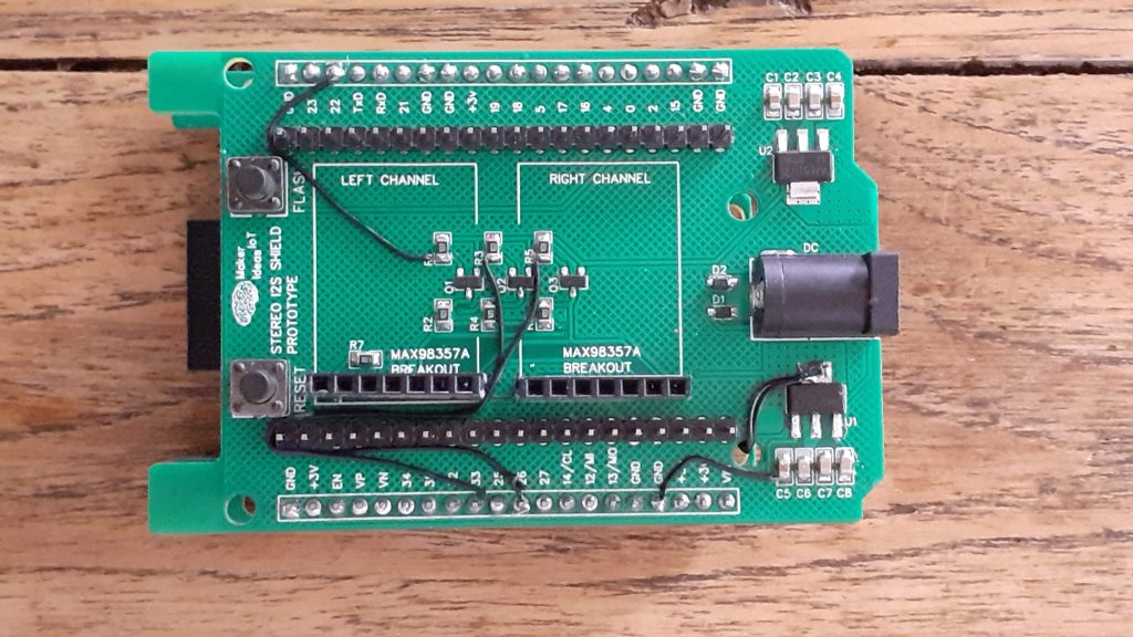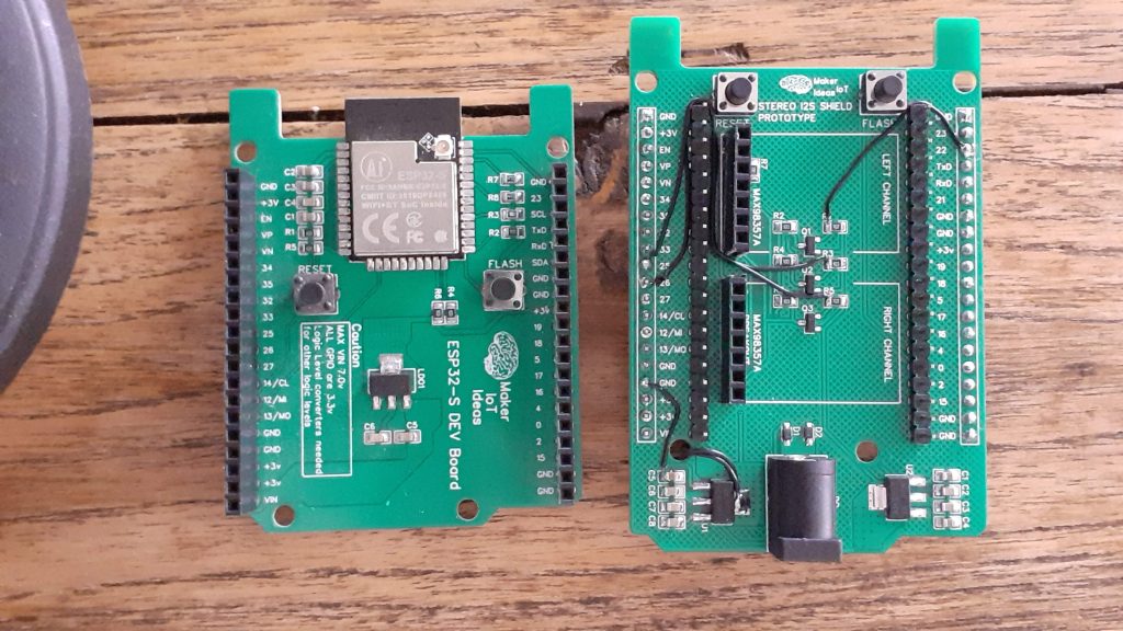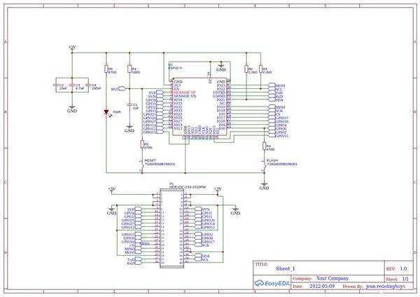
Last month I started working on a Stereo I2S Audio shield for my ESP32-S development board. Those of you that saw that post will remember that I made some mistakes on the initial prototype, and had to repair it with a few “greenwire” connections.
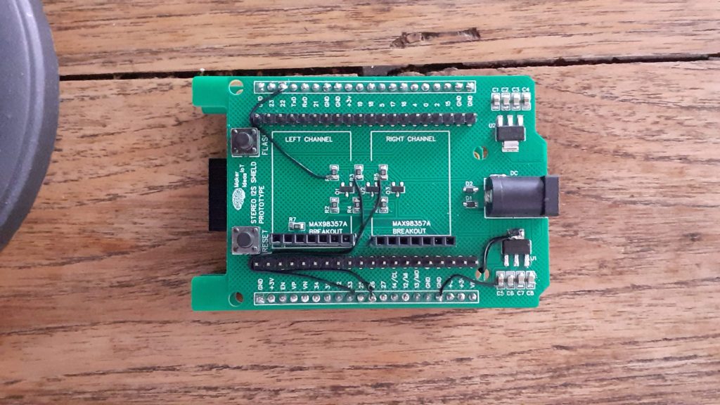
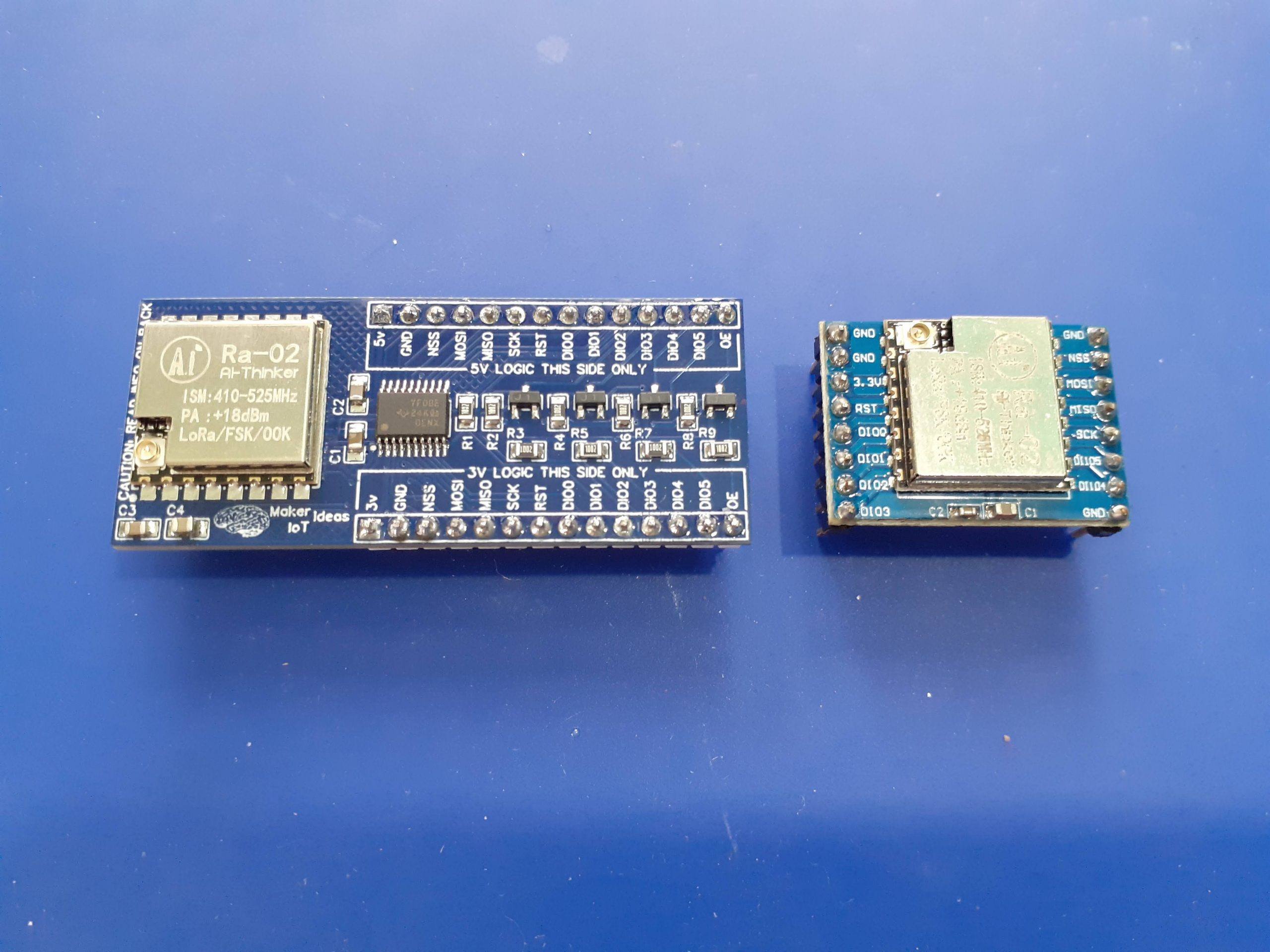
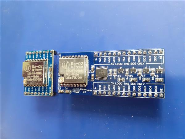
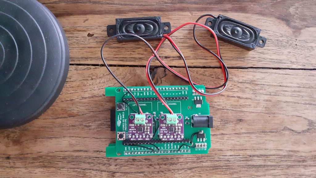
The prototype shield also required the use of commercial I2S modules to be plugged into it, making for quite a cumbersome first iteration.
I decided to do something about that, as the long-term use of this particular shield, as internet radio, with a further “dream” of using it as a remote media player for use from Home Assistant, is moving along well, with progress on the firmware being made slowly but surely.

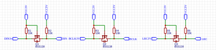
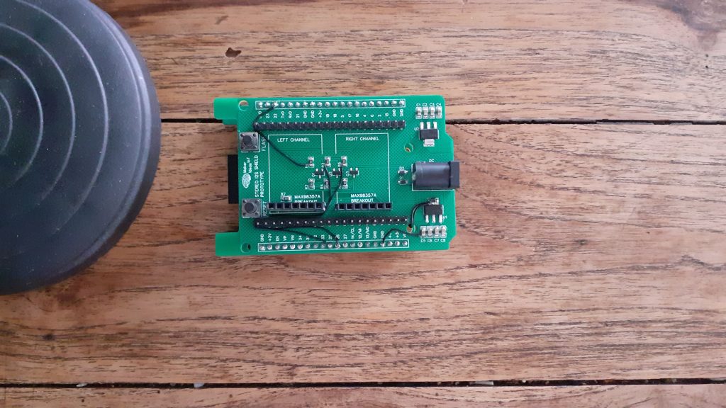
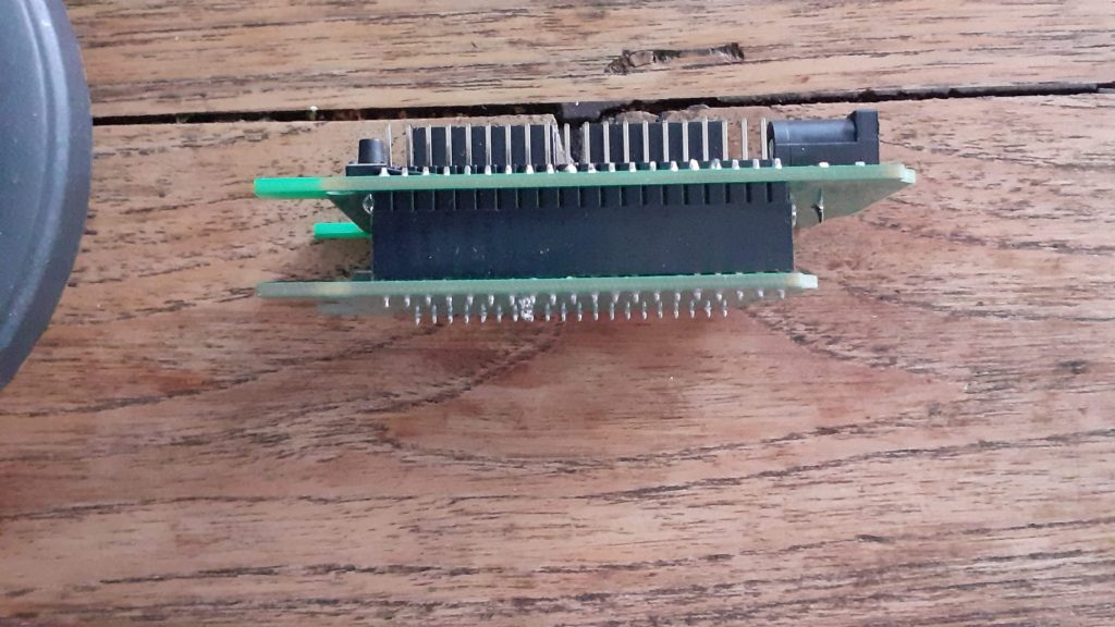
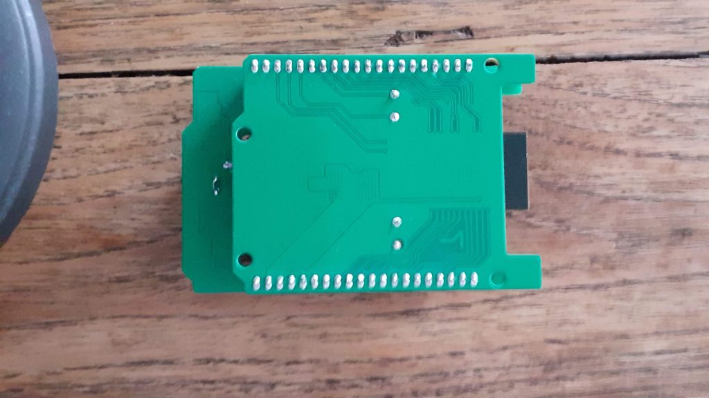
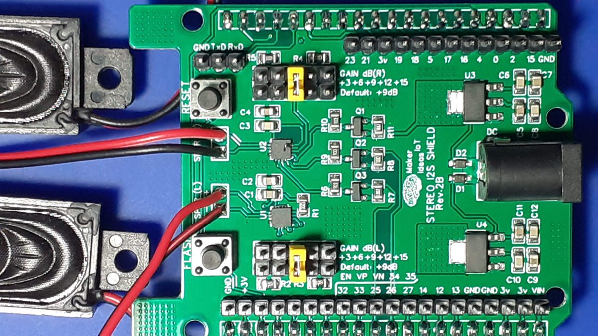
I decided that, since the Audio Chips seem to be quite easily available, and are modestly priced, getting rid of the plug-in modules, and placing the chips directly on the shield seemed like the next logical step. I also broke out the gain pins of each chip and made provision for easily changing said gain with a jumper, individually for the left and right channels of the I2S Audio shield.
I decided to keep the logic level conversion circuit, as it worked well, as well as provided another layer of protection to the ESP32-S that drives the whole shield. ( These have recently been discontinued by AI-Thinker, but the Espressif version is still begin manufactured and supported).
The power supply section of the board remains the same as the previous version, with a dedicated 5v regulator feeding the Audio section, and a 3v regulator the logic level converters. (I may change this in future, as the ESP32-S board can easily supply the 3v required without overloading the regulator on the CPU board.
Current issues that are carried over from the initial prototype still remain though. The two I2S Audion chips seem to be QUITE power-hungry, pulling almost 2A of current from a 12v supply, with a modest volume of 10 out of a possible 100. This has been reduced down from an earlier 4A to 6A when using a different pair of 4ohm 3W speakers.
This is also one of the reasons for the separate voltage regulators on the shield.
Manufacturing
I choose PCBWay for my PCB manufacturing. Why? What makes them different from the rest?
PCBWay‘s business goal is to be the most professional PCB manufacturer for prototyping and low-volume production work in the world. With more than a decade in the business, they are committed to meeting the needs of their customers from different industries in terms of quality, delivery, cost-effectiveness and any other demanding requests. As one of the most experienced PCB manufacturers and SMT Assemblers in China, they pride themselves to be our (the Makers) best business partners, as well as good friends in every aspect of our PCB manufacturing needs. They strive to make our R&D work easy and hassle-free.
How do they do that?
PCBWay is NOT a broker. That means that they do all manufacturing and assembly themselves, cutting out all the middlemen, and saving us money.
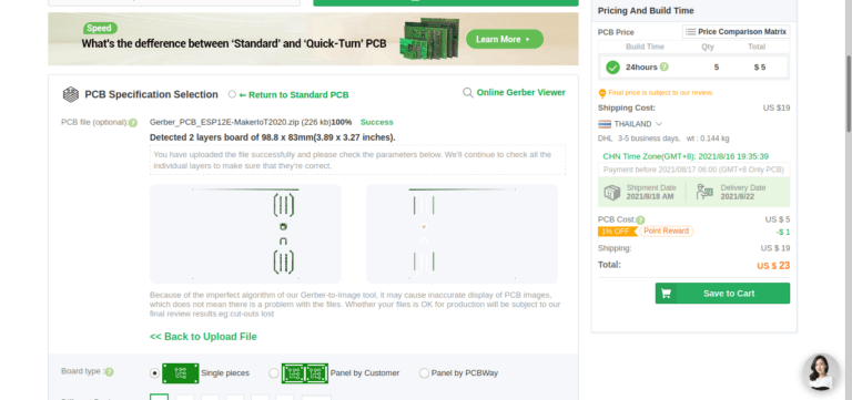
PCBWay’s online quoting system gives a very detailed and accurate picture of all costs upfront, including components and assembly costs. This saves a lot of time and hassle.
PCBWay gives you one-on-one customer support, that answers you in 5 minutes ( from the Website chat ), or by email within a few hours ( from your personal account manager). Issues are really resolved very quickly, not that there are many anyway, but, as we are all human, it is nice to know that when a gremlin rears its head, you have someone to talk to that will do his/her best to resolve your issue as soon as possible.
Find out more here

Assembly
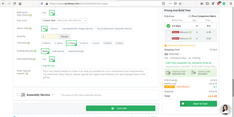
This project once again called for a stencil, as the QFN packages of the Audio chips are super tiny, with super tiny tracks and pads. A high-quality stencil definitely goes a long way in ensuring that just the right amount of solder paste is added to each pad. This also reduces the requirements for reworking a board with hot air to fix any solder bridges that might have formed.

The quality of a stencil says a lot about your PCB manufacturer, and in my case, I am extremely happy to say that PCBWay definitely delivers quality. Having used their services for close to 3 years now, I have not received a single faulty PCB or stencil at all. Yes, some PCB’s has had errors, but those were all MY errors. Design errors, not manufacturing errors.

Let us return to the assembly of this PCB, shall we…
As usual, the PCBs arrived very well packaged, and after a quick inspection and some random tests with a multimeter, It was time for solder paste and placing components, while listening to a piece of relaxing music… my way of relaxing…


After about 20 minutes of intense concentration, we have a PCB with all of the components correctly placed onto their respective pads, ready for reflow soldering.

I did things differently this time, by placing the QFN Audio chips in their positions at the same time as all the others. ( I usually drop them in place when the solder is in a liquid state, but with these, I was confident in the stencil, and as these chips were quite a bit more expensive than my usual projects [ over 3 USD each ], I wanted them to slowly get up to temperature, and spend as little time as possible at temperature as well. )

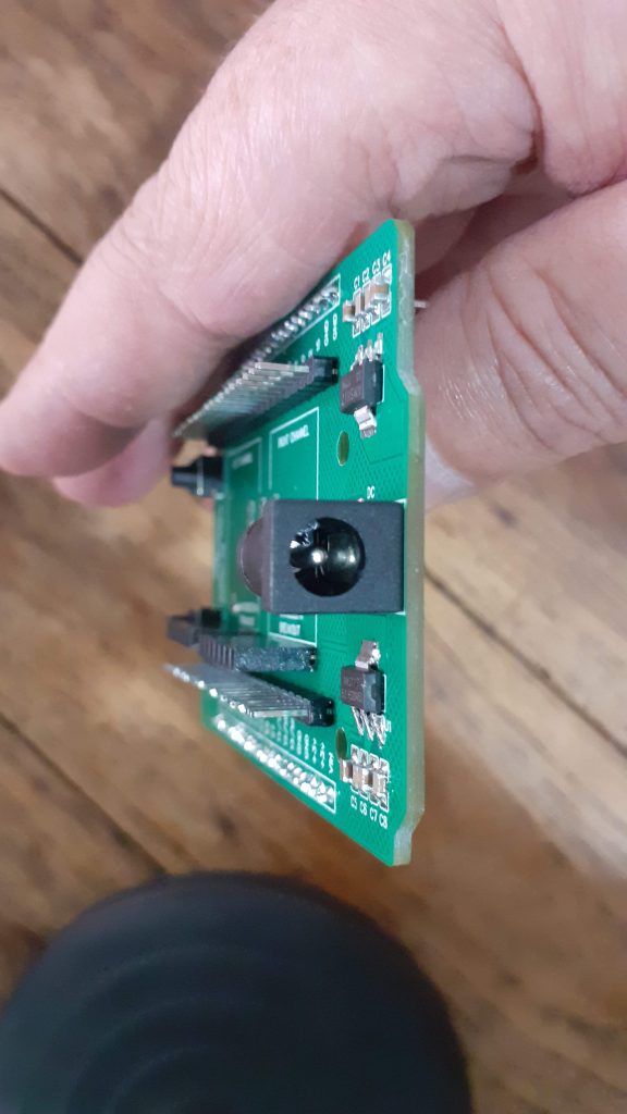
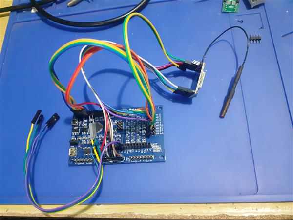
Reflowing was a success, and after inspection, no solder bridges were found. A detailed diagnostic with a multimeter with fine-tipped needle probes confirmed that there were no short circuits or bridges, and I could thus continue with the rest of the assembly – the various through-hole components, being mostly header pins, switches and a DC barrel jack socket.

The speaker wires were soldered directly to the PCB, due to the fact that being a prototype, I did not see the need to raise the cost even more by adding connectors onto a board that may not be used very long if it turns out that there is a problem somewhere.
Testing
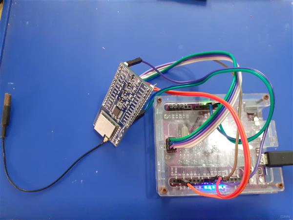
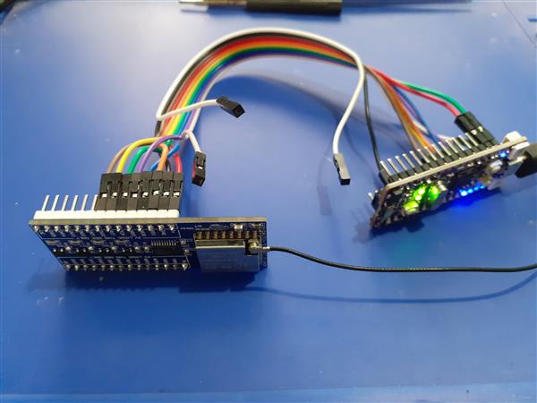
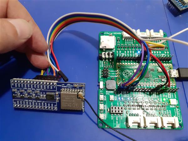
The next stage was testing, using the software provided in the initial Stereo I2S Shield post. All went well, but, as mentioned above, I encountered the same high current draw issue, which resolved itself ( in a manner of speaking ) after I reduced the initial startup volume of the unit, and limited the maximum volume in the software.
I can now continue with firmware development, and sort out things like the rotary encoders for the volume and station selection, as well as look at adding an i2c display, and possibly a sd-card for stored music files.
Conclusion
The project is getting along quite well, and this iteration of the prototype did not have any design faults or errors. I am extremely impressed with the reliability of my PCB manufacturer, as their consistent quality products allow me to focus on design, and trust that whatever comes back from the factory will be exactly as I designed it.
While there are still quite a few issues to sort out on this project, I am confident that in the end, it will all turn out the way that I want it to.