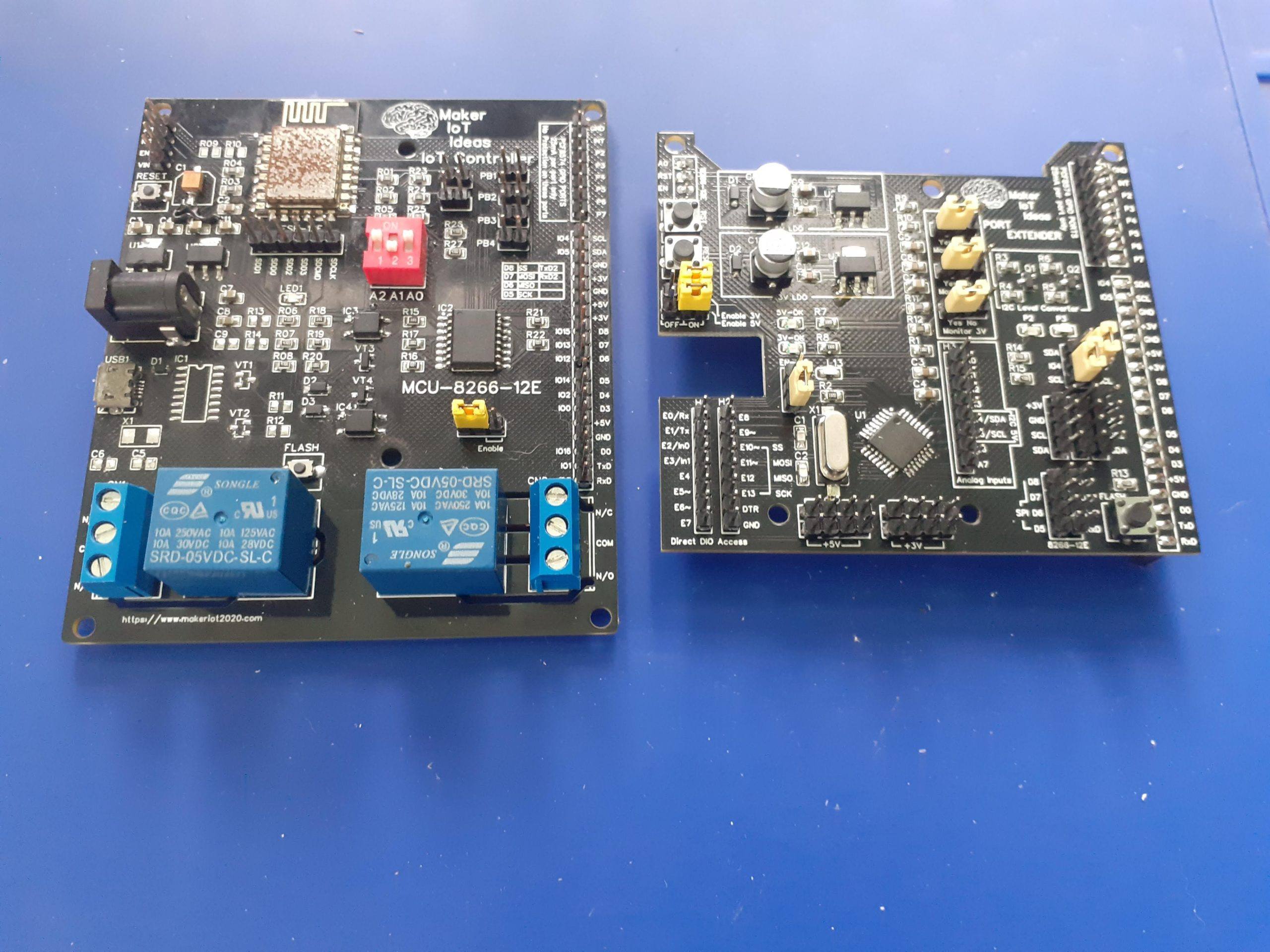
ATMEGA328P Module with integrated LoRa and CAN-BUS
INTRODUCTION
In my quest to perfect my LoRa telemetry system, I have gone through quite a few prototypes by this time. This post will focus on the next node design. Due to the fact that the area where I will deploy the system is quite large, but with roughly square boundary fence-lines, I decided to try and reduce the number of LoRa Radio nodes needed to cover the entire area. This opened up the opportunity to utilise CAN-BUS to attach sensor-only nodes to a Radio node and have them report status on exception as well as on requests from the radio node.
The device will thus function as a LoRa-to-CAN-BUS Gateway, with some local automation to control the transmission of data to the master station. This concept can also be adapted for use in other areas, such as home -automation, or an industrial setting.
At the heart of the device, I have stuck with the versatile ATMEGA328P, which, current chip shortages excluded, and current high prices excluded, are a very inexpensive chip, with lots of well-tested libraries, and a relatively low learning curve, largely due to its very wide use in the Arduino ecosystem.
The LoRa component is handled by the RA-02 or even RA-01H module, from AI-Tinker (not sponsored). This device, as we have seen in the previous prototypes, requires the use of logic level converters, due to the fact that it only accepts 3.3v logic levels. While I could get rid of those if I powered the ATMEGA328P from 3.3v, it would give rise to two problems, of which one will still force the use of level converters…
I chose to run the ATMEGA328P at 16Mhz, which basically forces me to use 5v to power the chip. The second reason is not so obvious unless you read a few datasheets very thoroughly…
The CAN-Bus component is handled by the MCP2515 Standalone SPI-to-CAN Controller, as well as the TJA1050 CAN Bus transceiver.
This is where things get interesting… The MCP2515 can operate on 3.3v, but the TJA1050 is a 5v only device. I could thus in theory use logic level converters only between the MCP2515 and the TJA1050, while running the rest of the circuit on 3.3v…
Given that I would rather run the ATMEGA328P on 16Mhz, as well as the fact that my LoRa Radio Module circuit, with its logic level converter circuitry, works extremely well, I decided not to change that, and keep the CAN Bus running at 5v all the way through, as I would still have to use a 5v regulator on the PCB anyway just for that purpose.
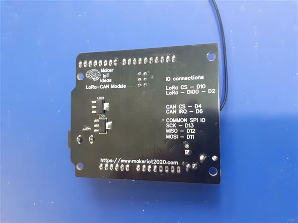
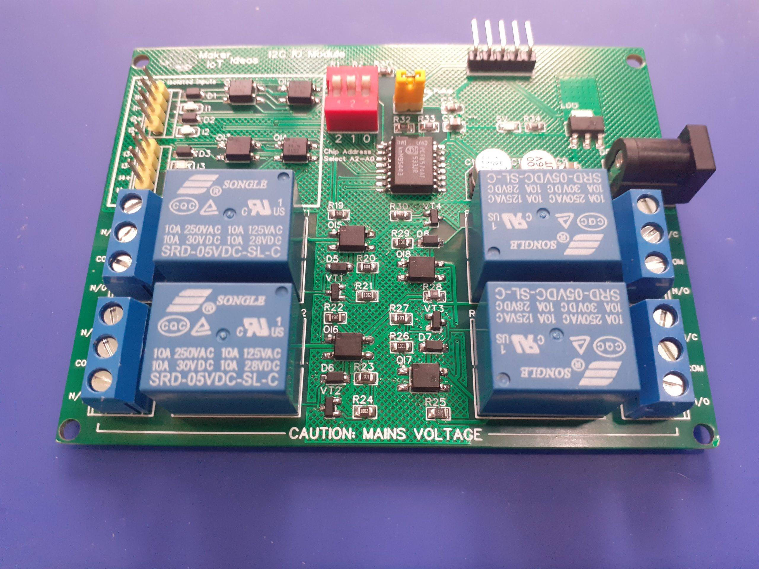
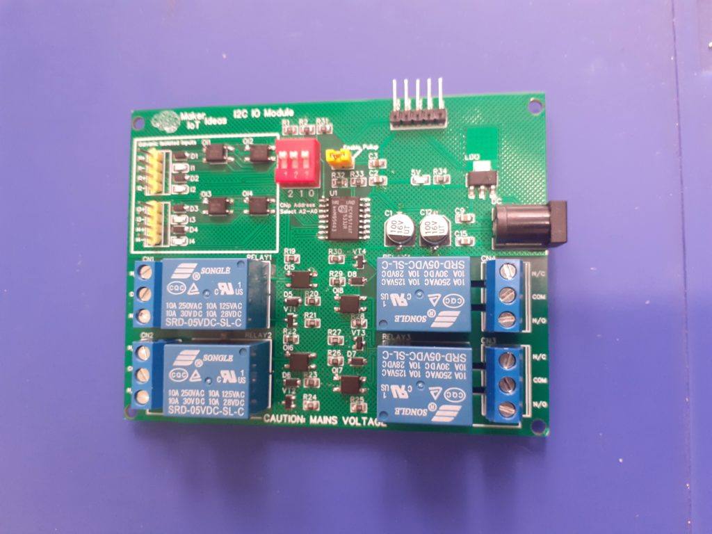
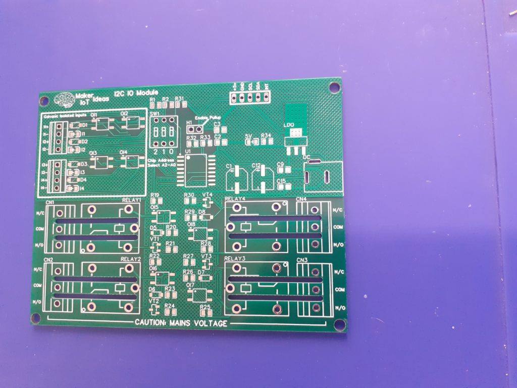
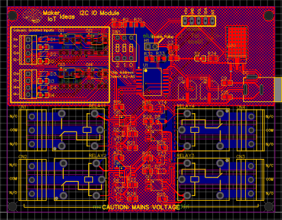
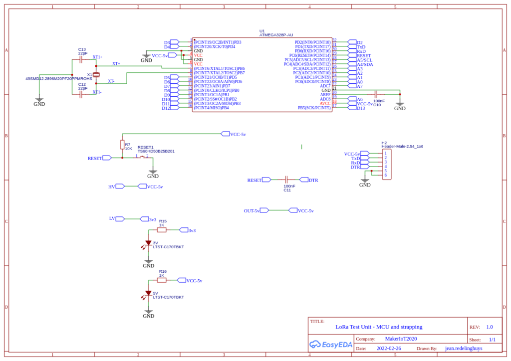
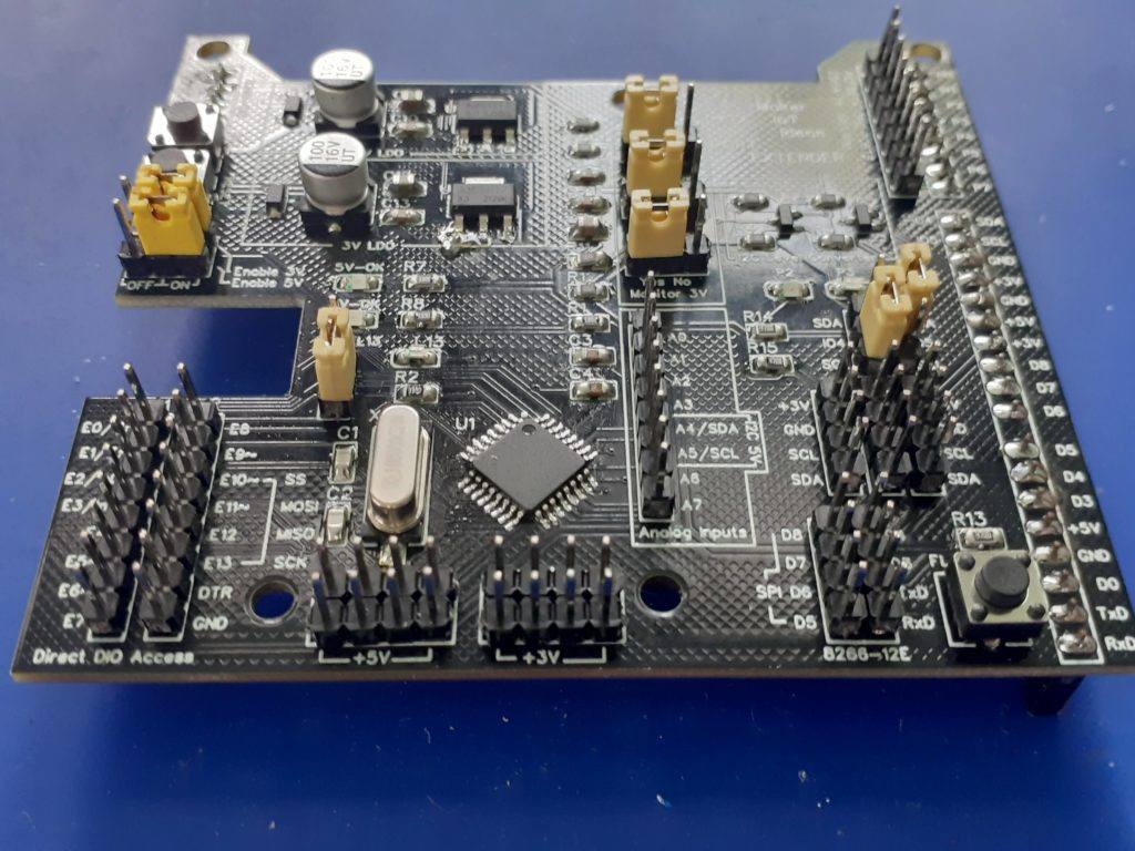
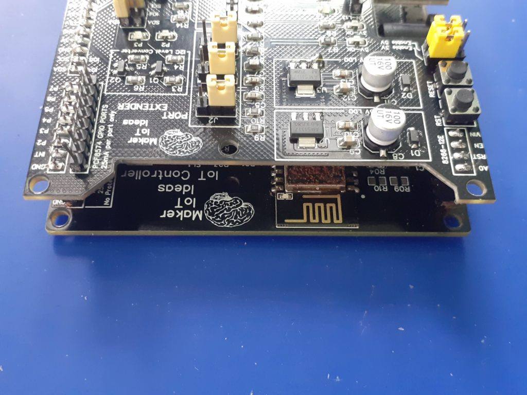
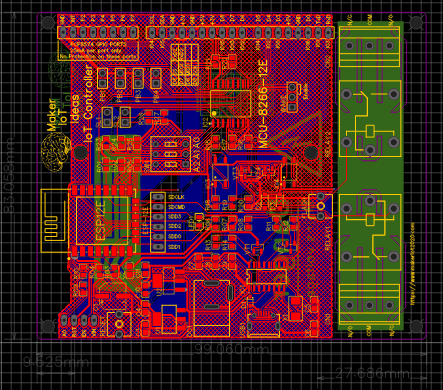
IO connections for LoRa and CAN BUS modules

You can order this PCB directly from PCBWay, by clicking here
Both of the two integrated components ( Lora and CAN ) are SPI devices. This means that they share common SCK, MISO and MOSI lines ( provided on the ATMEGA328P by pins D13, D12 and D11 respectively. The individual SPI device is then further selected for operation by the use of a CE pin, one unique pin per device, which is pulled low by the MCU to indicate to the device that it should pay attention to the data being transmitted on the SPI bus…
Both LoRa and CAN makes use of other pins as well, LoRa needs a Reset pin, connected to D9, a CS/CE Pin on D10 as well as a hardware interrupt pin, connected to D2. ( Note that this is for use with Sandeep Mistry’s LoRa Library. The Radiolib library would require an additional pin, usually connected to DIO1 on the LoRa module. The device does not provide access to those pins in its current layout, so you can only use it with the Sandeep Mistry library, for now at least… )
The CAN module uses a CE/CS pin at D4, with an IRQ pin on D6, which, although not a hardware interrupt pin, does have PCINT functionality.
Pins D10, D9 and D2 are not broken out for user access. although I decided to give access to D4 and D6, as well as the SPI bus, D11, D12, D13, to allow interfacing with logic analysers, or adding other SPI devices to the bus…
This brings us to a very interesting point… Does the two SPI devices actually play nice together? and what do I mean by “playing nice together”?
To answer that question, we are forced to first look at a bit of theory, as well as understand the fundamental differences between SPI and I2C…
The Difference between SPI and I2C
Most of us will be quite familiar with I2C, as it is a very common protocol used to connect sensors to a microcontroller. It consists of only two IO lines, SDA for data, and SCL for the clock. Each device on the bus has its own built-in address, like in the case of a PCF8574 IO expander, this address can be selectable between 0x20h and 0x27h. All of the devices share these common data lines, and will only respond when specifically addressed by the master controller… Unless you accidentally put two devices with the same address on the same bus, (if that would even work), there is no way that the wrong device would respond to any request for data…
SPI on the other hand, operates on a completely different principle, making it quite a few times faster than I2c, with data being simultaneously sent and received by the active device… SPI is also known as a four-wire protocol. Each device has a minimum of 4 data lines, namely SCK ( clock), MOSI ( for data transmitted FROM the Master TO the slave device ), MISO ( for data transmitted TO the master FROM the slave device) and a CE or CS ( Chip select ) pin.
SCK, MISO and MOSI are COMMON to all devices, meaning it is shared between all of them. CE/CS is a unique pin for EACH device, meaning that if you had four SPI devices on a bus, you would have to have four individual CE/CS pins!
A device will, or rather should only respond to data on the SPI-BUS IF the master pulls its respective CE/CS pin LOW. It should now very quickly become clear to you that this can become a very very complex mess, very quickly.
Let us take a very good example. the ST7789 SPI display module, has a cheap version, commonly sold on Ali-express, as we ll as other online stores. This particular module, I assume in a bid to make it easier to use, has the CE/CS pin internally pulled down to ground by default… So what about that, you may ask? What is wrong with that, as it saves you an IO pin?
It is in fact very wrong, a fact that you will very quickly discover if you ever tried using one of those displays on an SPI bus together with other SPI devices… Nothing will work, or only the display will work ( if you are lucky)
But why?
Pulling CE/CS LOW, signals to the chip that it should respond to instructions on the common SCK, MISO and MOSI lines. having the pin internally pulled LOW, thus forces that chip to always respond, even when it should not. Thus contaminating the entire SPI-BUS with garbage…
The answer to the question
After that very long-winded explanation, which is still extremely basic, it is time that we get back to our original question:
Does the Sx127x ( RA-02 ) Module and the MCP2515 Can Controller play nice on the same bus? The answer is not straightforward, as it comes down to which libraries you use…
Remember that the library must pull down the CE/CS pin of the device that it wants to communicate with. Some libraries wrongly assume that they are the only ones in use, and ignores the simple fact, that they should release the CE/CS pin AFTER EVERY transaction, to free up the bus for other devices to use it as well…
After extensive testing, I can however say that Sandeep Mistry’s LoRa Library, as well as the mcp_can library, does indeed play nice together. These two libraries do not keep the individual CE/CS pins pulled LOW, and allows the spi bus to be shared.
This is not the case with the ST7789 Module discussed above, where the hardware actually pulls the pin ow the entire time…
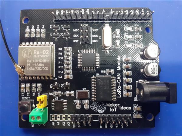
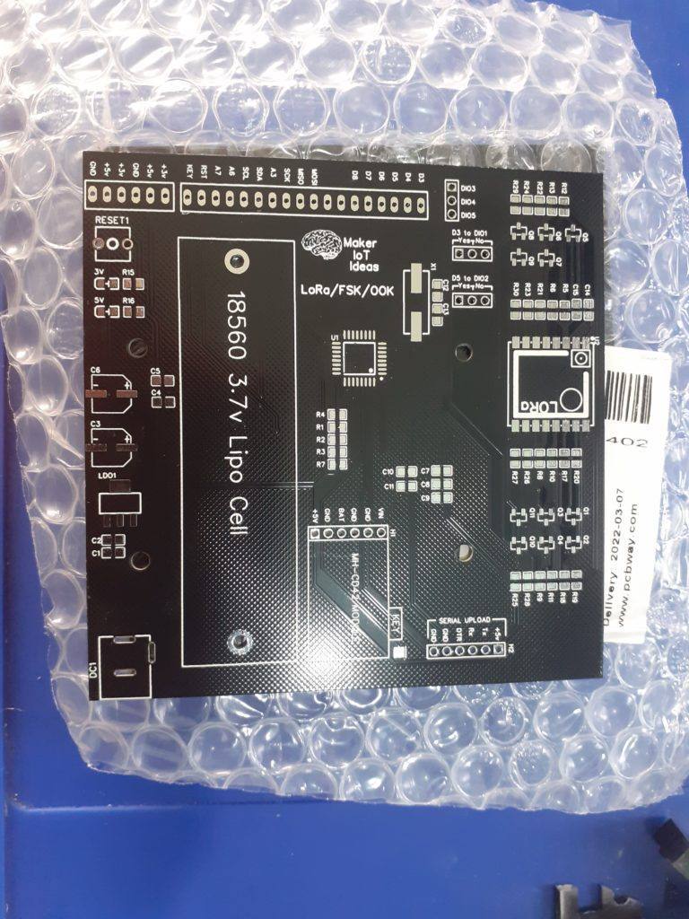
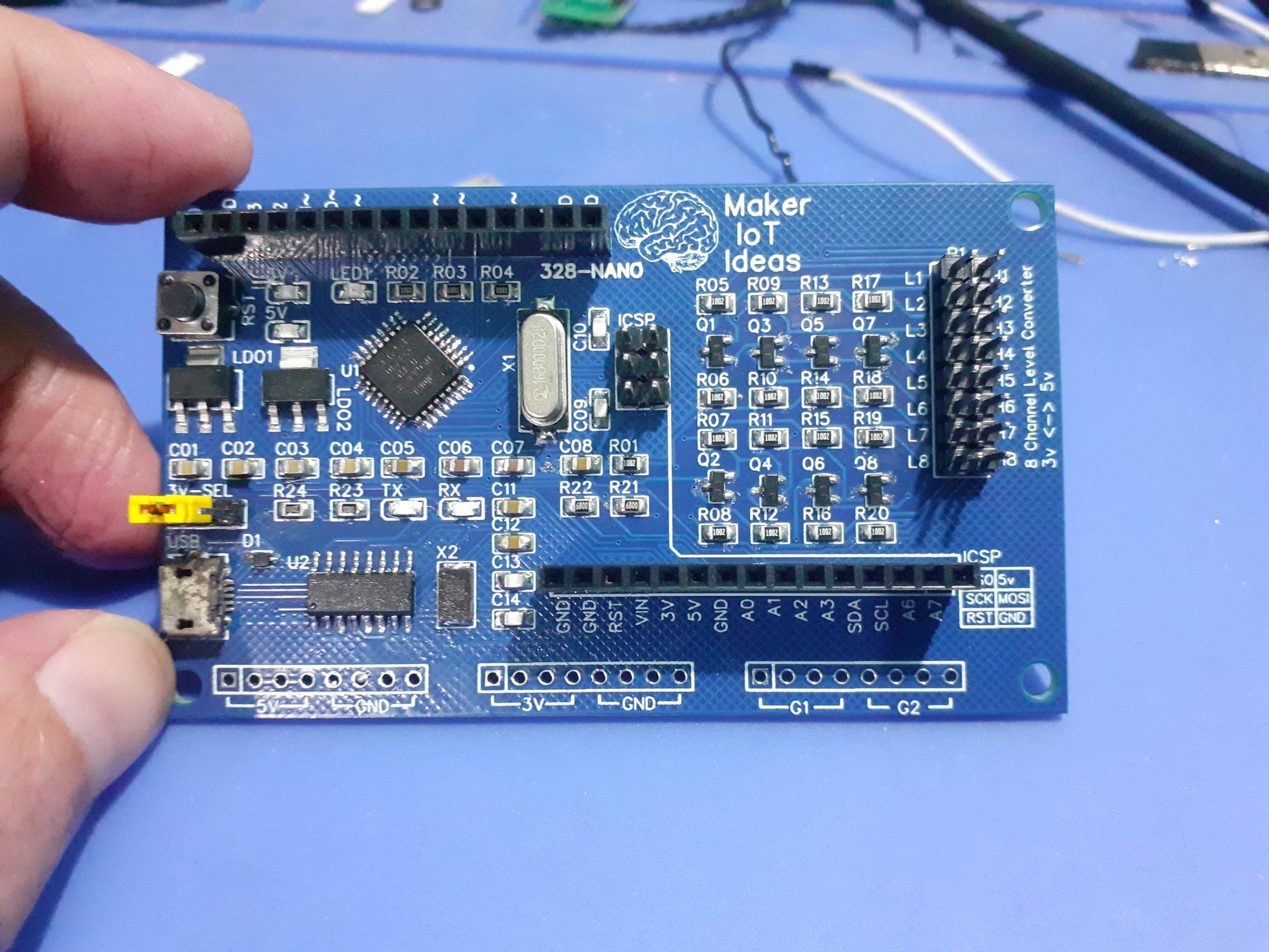
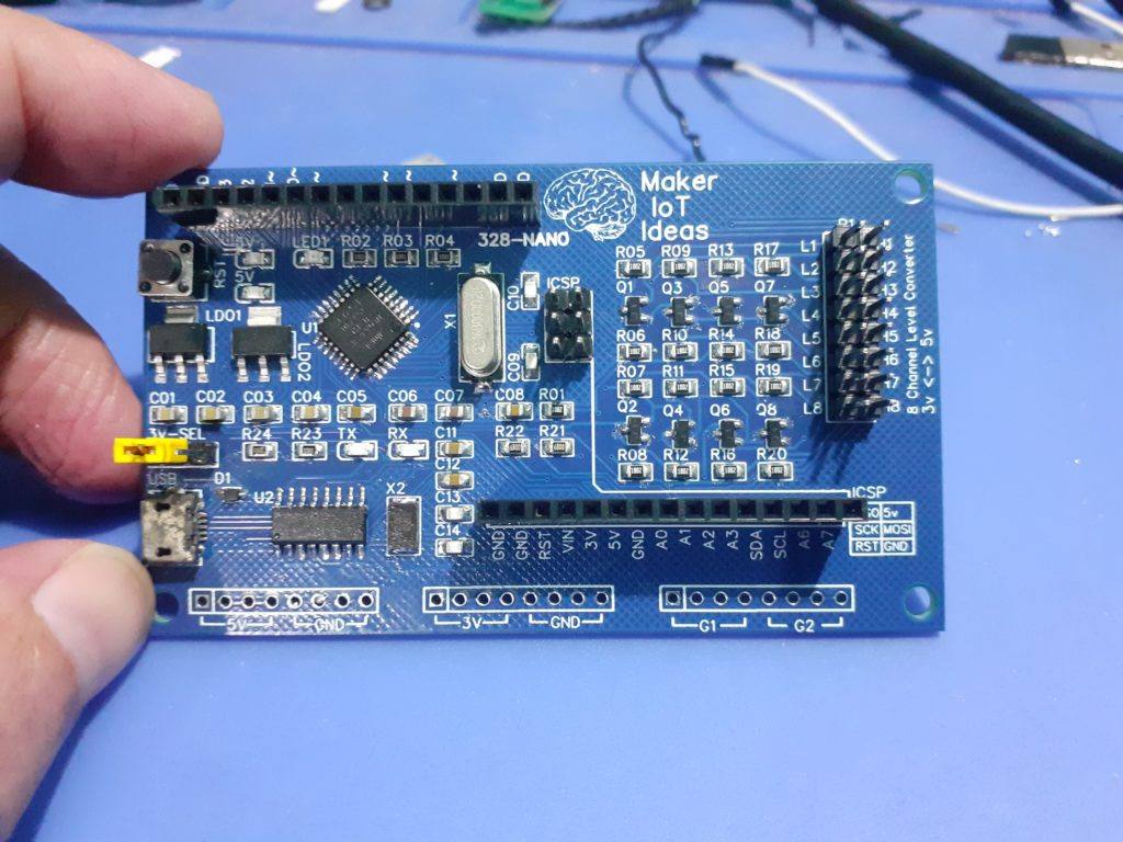
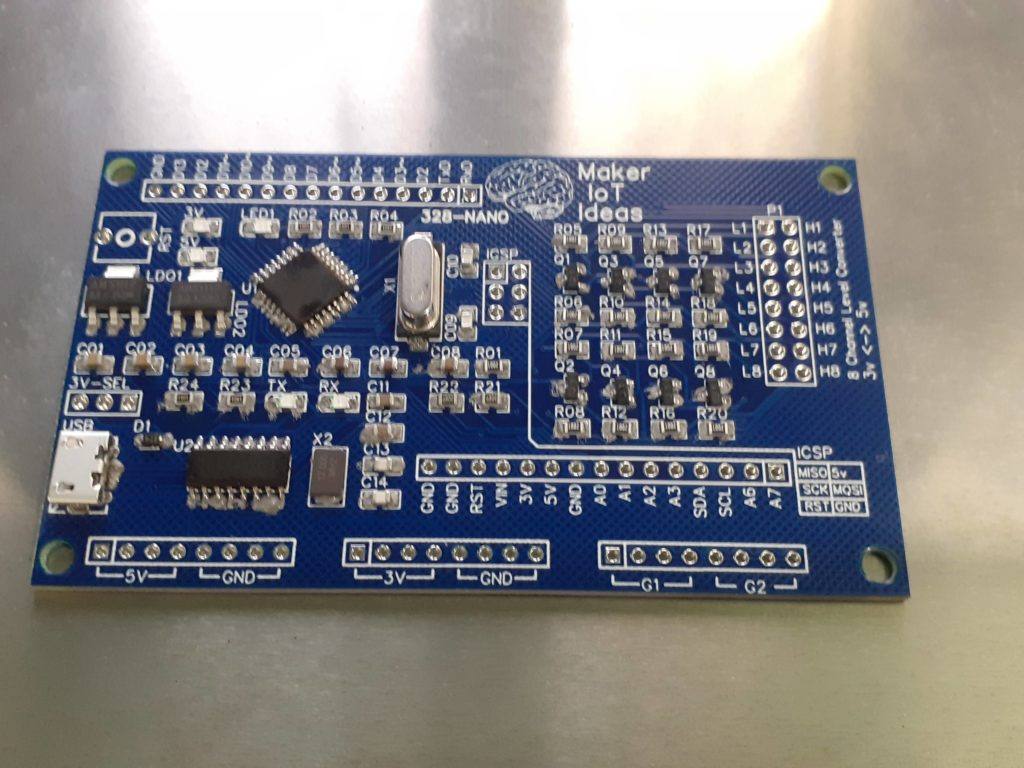
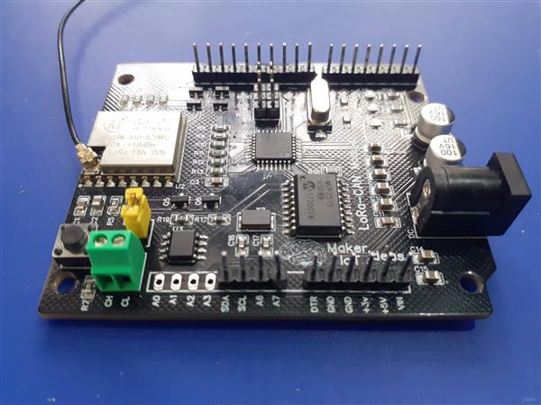
Taking a closer look at the PCB
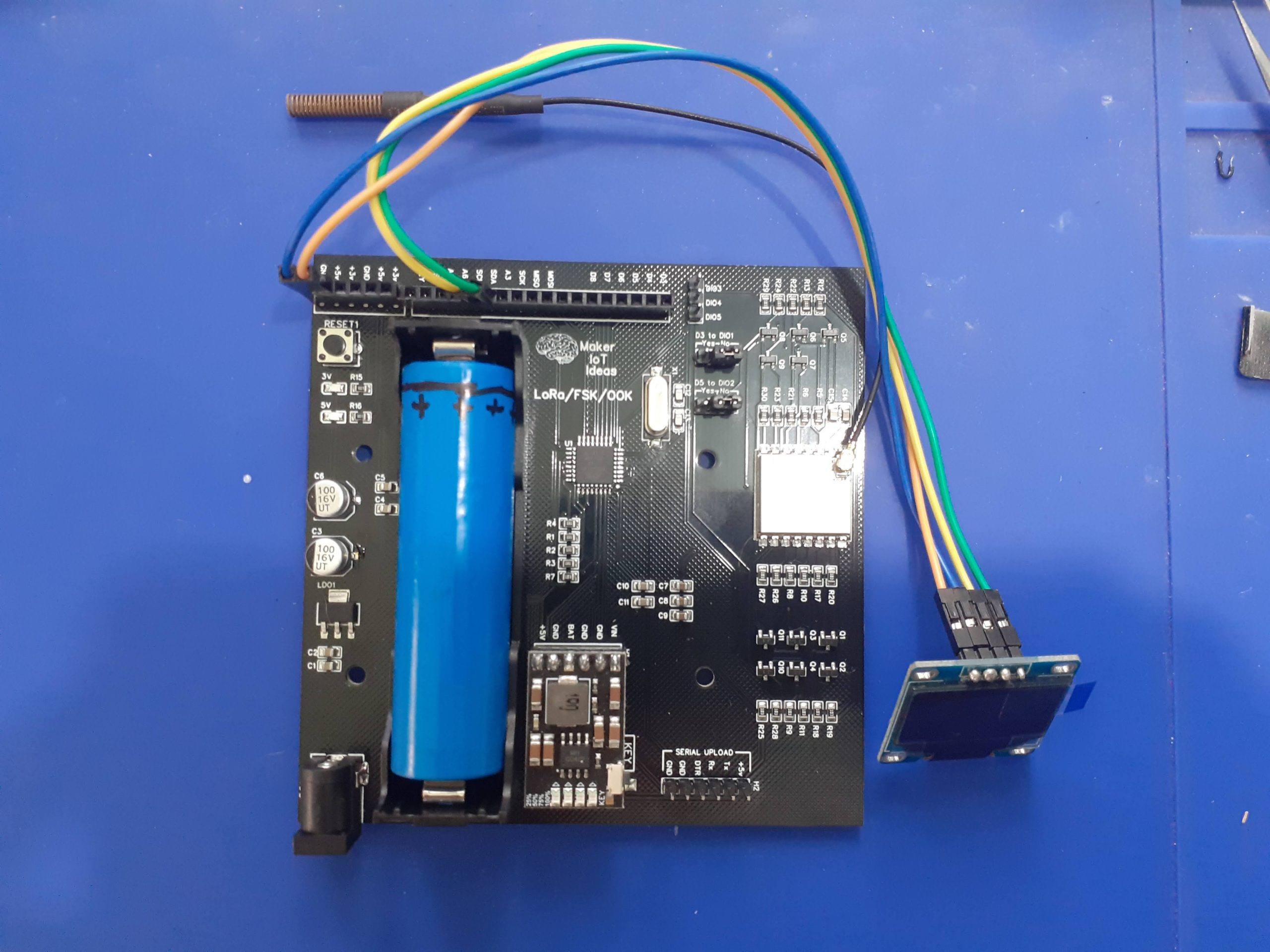
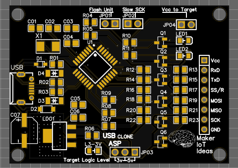
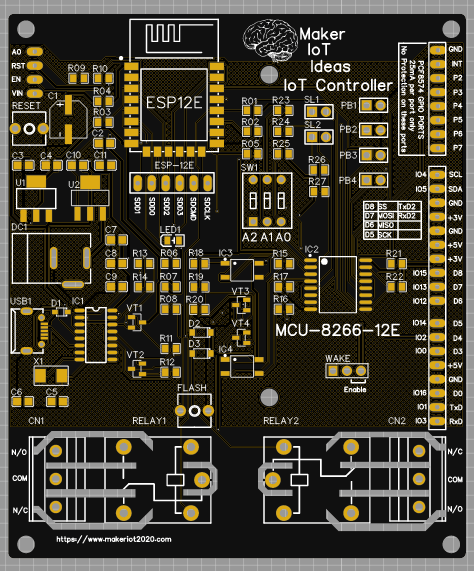
Let us take a closer look at the PCB. The Ra-02 Module ( LoRa ) dominates most of the left-hand side of the PCB, with the ATMEGA328P on its right. The RA-02 is surrounded by the level converters, using the BSS138 N-Channel Mosfet, and 10k resistors (Q1 to Q6, R1, R2, R3, R4, R5, R6, R8, R9, R10, R11, R12, R13)
C1 and C2 are bypass capacitors for the Ra-02 module
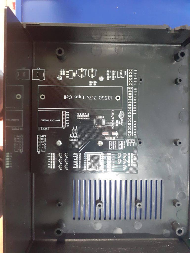
In the bottom left corner, we have a hardware reset button, to reset the ATMEGA328P, with a yellow jumper (H1) next to it. This jumper controls the 120ohm ballast resistor (R17) for the CAN bus. Removing the jumper will remove the ballast. Directly below that is the CAN connecter, marked as U5, with CH as CAN-H, and CL as CAN-L ports.
U3 and U4, together with R18, R19, X2, C16, C17 make up the CAN components on the PCB. Decoupling is provided by C6, C7, C8 as well as C9 and C12 ( Includes the ATMEGA328P’s decoupling as well )
An ICSP programming header is provided above U1 ( ATMEGA328P) for use with USPASP, AVRASP or Arduino as ISP and similar.
No USB to serial converter is provided on the board, Serial upload is possible is loaded with an Arduino bootloader for the Arduino NANO ( to make use of all the analog inputs). RxD, TxD and DTR pins are broken out on opposite sides of the PCB, as well as access to 3.3v, 5v and GND pins.
A DC power socket is provided. it can accept up to 12v DC, although I would recommend not to go over 7.2 volts, to not stress the LDO regulators, at the back of the PCB ( LDO1, and LDO2) too much.
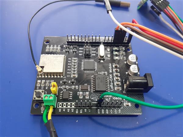
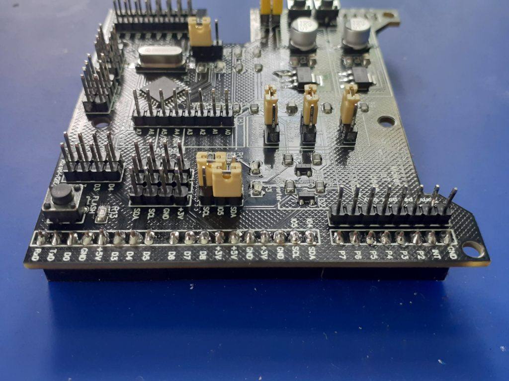
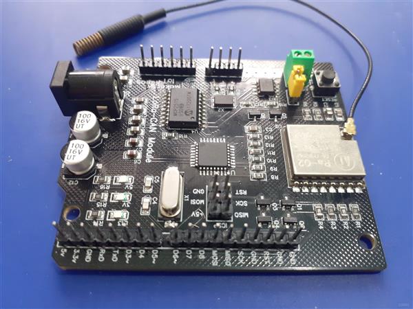
in the picture above, I have connected a USB-to Serial converter, as well as CAN-BUS to the device.
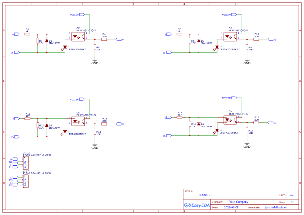
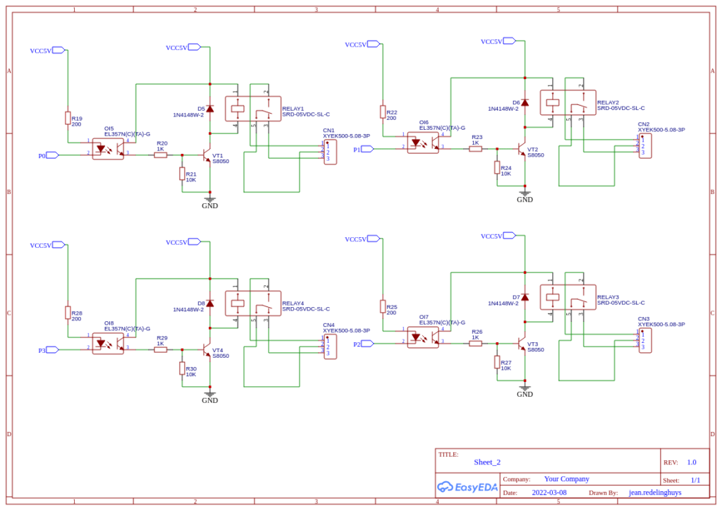
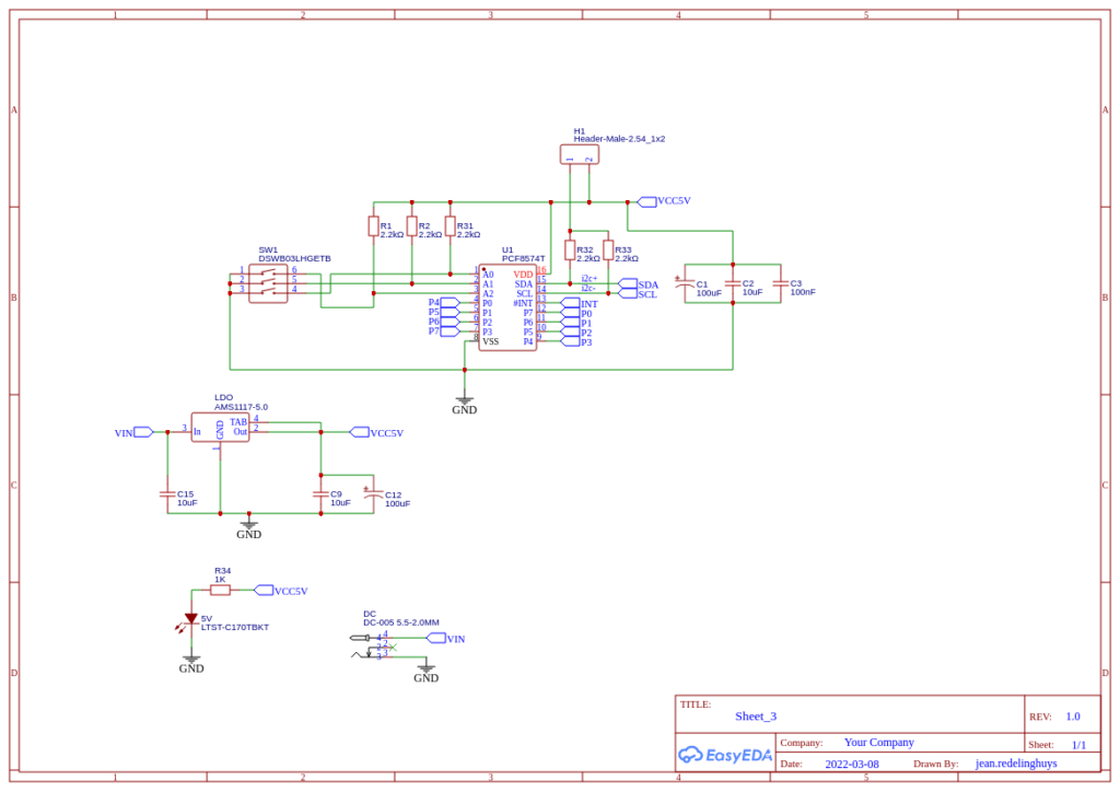
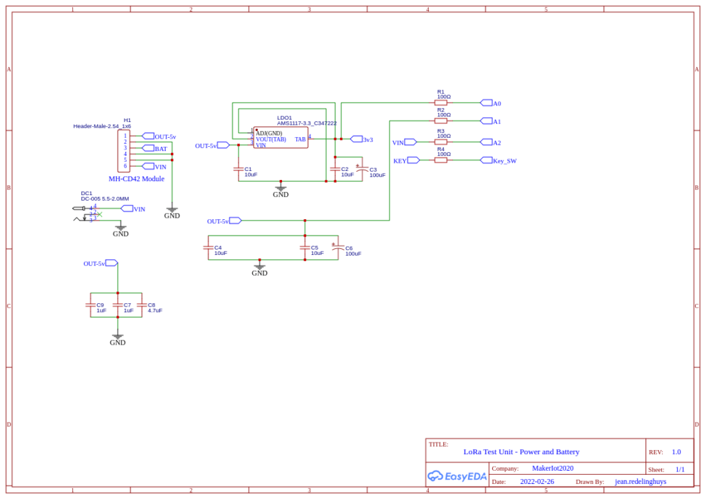
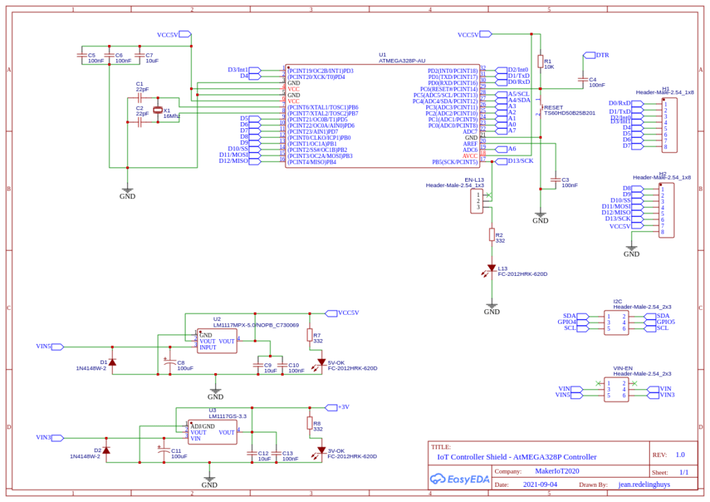
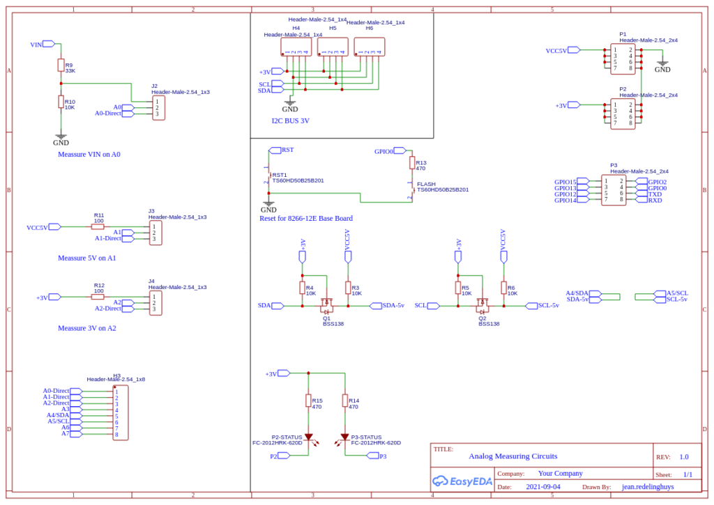
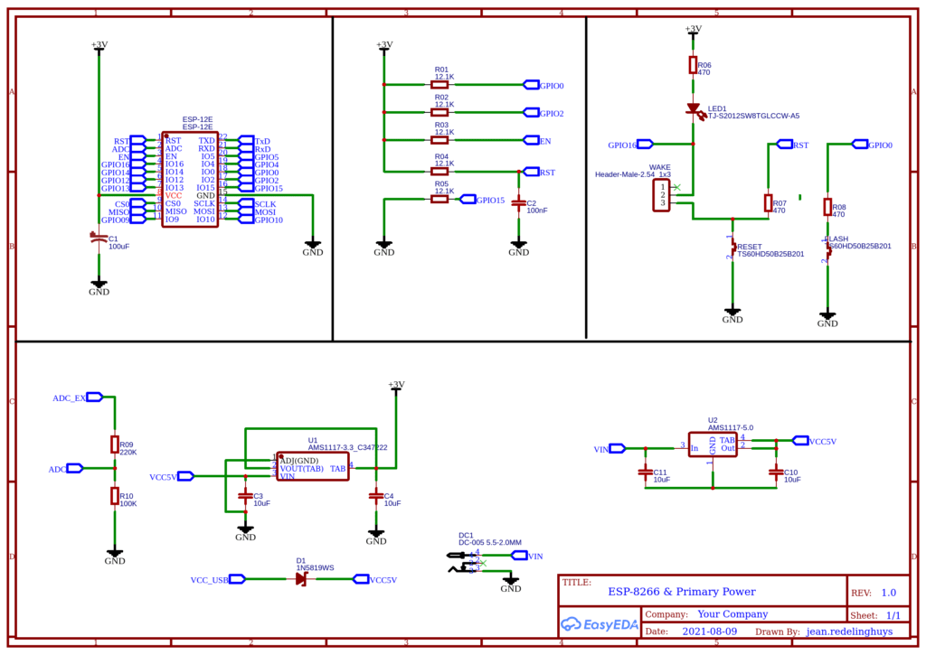
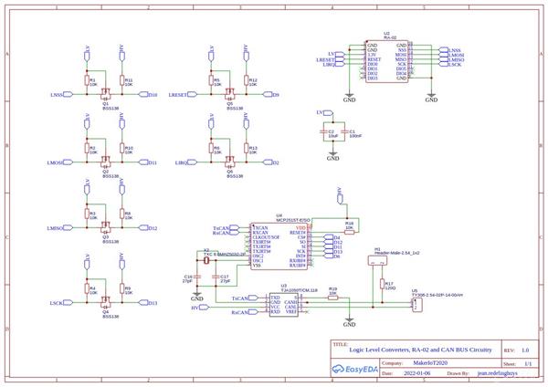
Schematic Diagram
The detailed schematic diagrams are provided below:
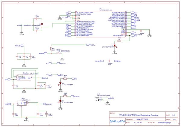
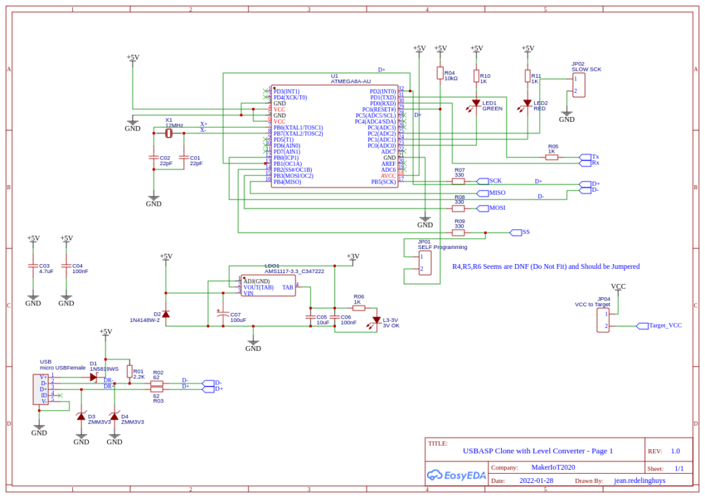
Sheet 1 (above) takes care of the ATMEGA328p and it supporting circuitry, as well as the power supply via LDO regulators.
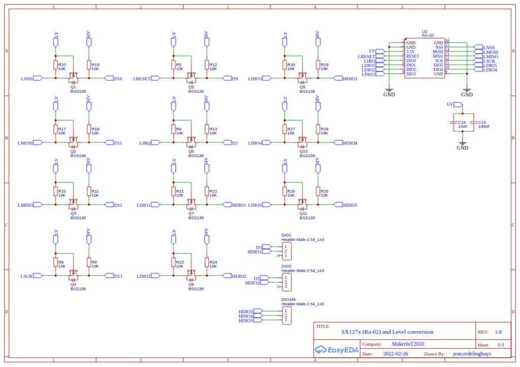
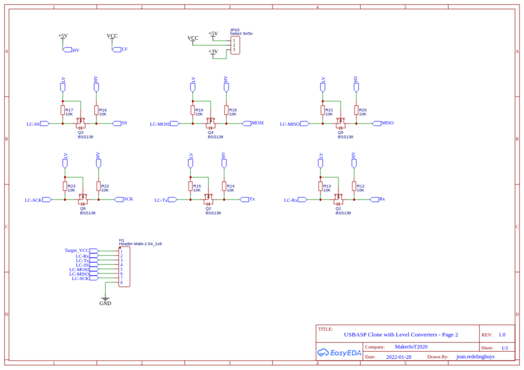
Sheet 2 (below) takes care of the Logic Level converters, RA-02 (Sx1278) LoRa Module, and CAN-BUS controller and transceiver circuitry.
Software and Firmware
In order to test this module, I made use of the mcp_can library by Cory J Fowler, for the CAN-Bus part,
as well as Arduino-LoRa by Sandeep Mistry
A combined example utilising both LoRa and CAN at the same time, will be released with the next part of the project, namely the CAN-Relay Module
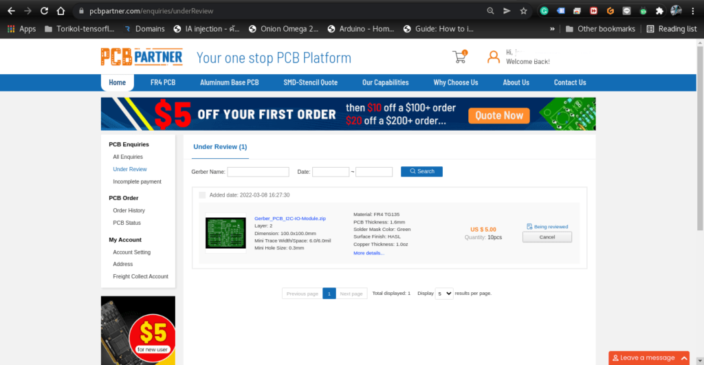
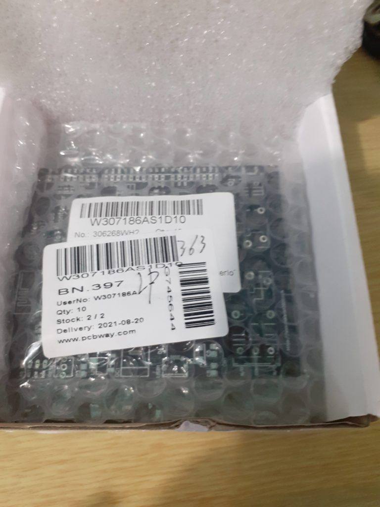
This PCB was manufactured at PCBWAY. The Gerber files and BOM, as well as all the schematics, will soon be available as a shared project on their website. If you would like to have PCBWAY manufacture one of your own, designs, or even this particular PCB, you need to do the following…
1) Click on this link
2) Create an account if you have not already got one of your own.
If you use the link above, you will also instantly receive a $5USD coupon, which you can use on your first or any other order later. (Disclaimer: I will earn a small referral fee from PCBWay. This referral fee will not affect the cost of your order, nor will you pay any part thereof.)
3) Once you have gone to their website, and created an account, or login with your existing account,
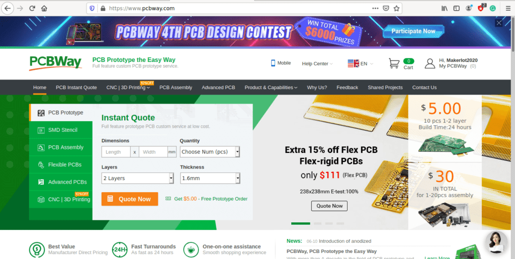
4) Click on PCB Instant Quote
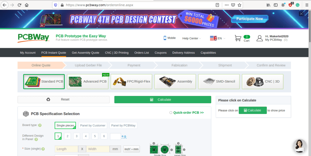
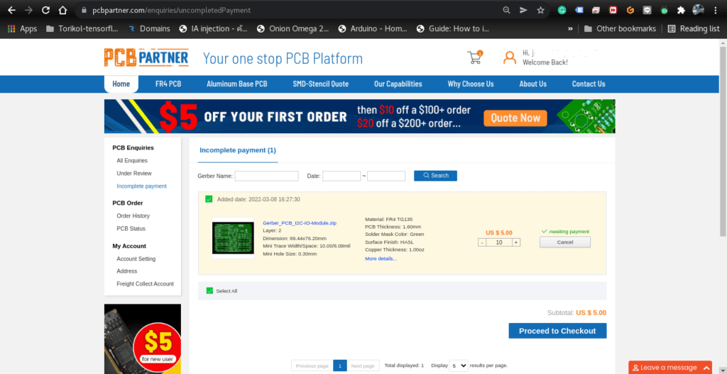
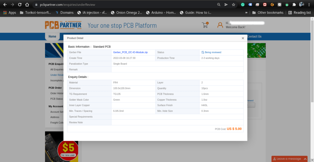
5) If you do not have any very special requirements for your PCB, click on Quick-order PCB
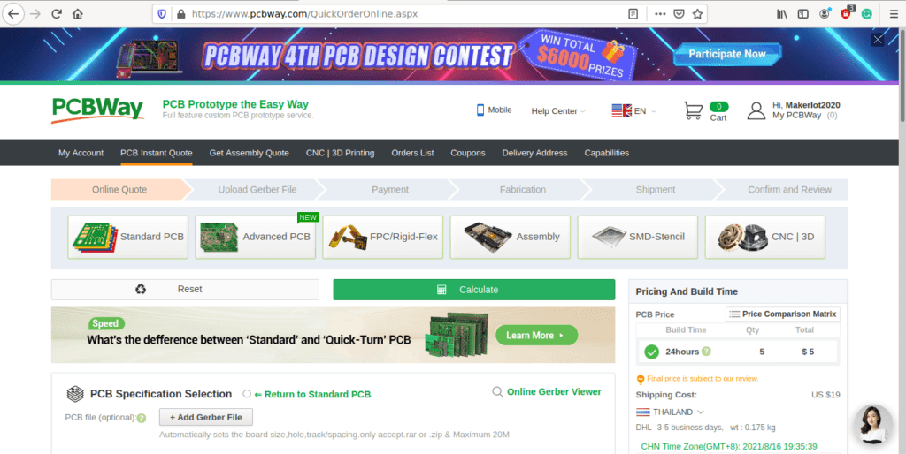
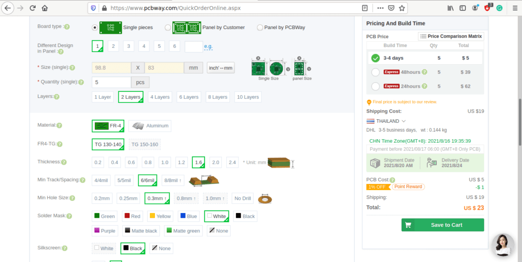
6) Click on Add Gerber File, and select your Gerber file(s) from your computer. Most of your PCB details will now be automatically selected, leaving you to only select the solder mask and silk-screen colour, as well as to remove the order number or not. You can of course fine-tune everything exactly as you want as well.
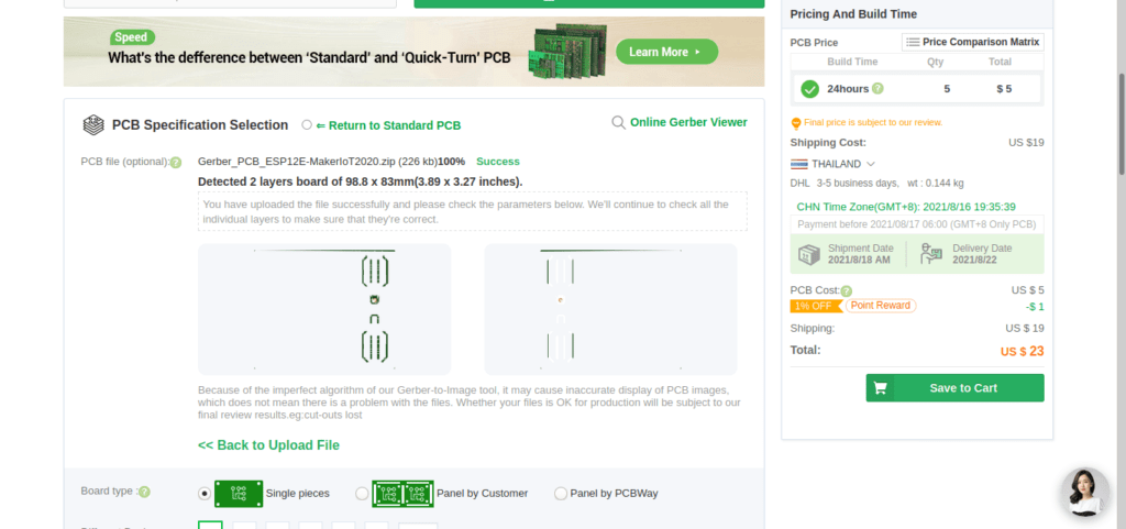
7) You can also select whether you want an SMD stencil, or have the board assembled after manufacturing. Please note that the assembly service, as well as the cost of your components, ARE NOT included in the initial quoted price. ( The quote will update depending on what options you select ).
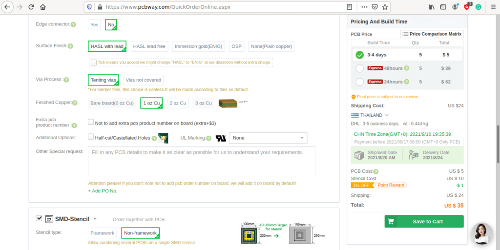
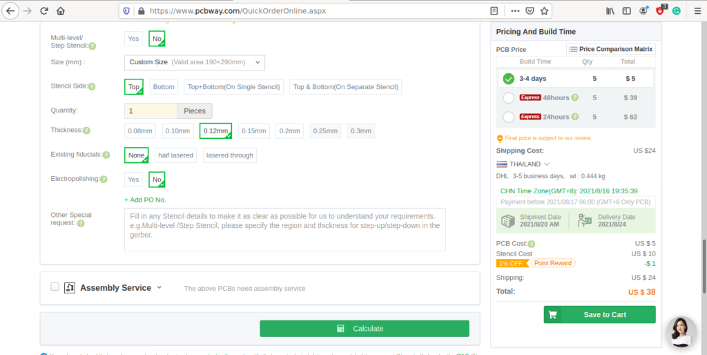
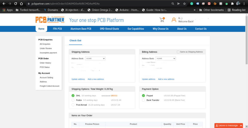
8) When you are happy with the options that you have selected, you can click on the Save to Cart Button. From here on, you can go to the top of the screen, click on Cart, make any payment(s) or use any coupons that you have in your account.
Then just sit back and wait for your new PCB to be delivered to your door via the shipping company that you have selected during checkout.