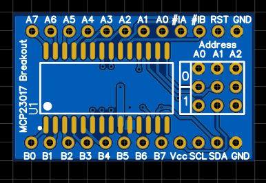
I2C port extenders or expanders are extremely useful devices, and I use quite a lot of them in my projects. My go-to device is definitely the PCF8574, mainly because it is sort of “breadboard friendly”. The MCP23017, with the existing breakouts available locally, are not. I have thus decided to design my own version of a breadboard friendly MCP23017 breakout board.
The Breakout Module PCB and its features
A breadboard friendly MCP23017 breakout board – Fronta breadboard friendly MCP23017 breakout board – Back
While this was definitely one of my easier projects, It still took a bit of time to get it just right and add some essential components and features directly onto the PCB.
The main features of this breakout: – DIP12 Layout – with all pins broken out, address pins to jumper headers… – Proper decoupling capacitors, as close as possible to the MCP23017 chip. I had to make use of the back layer of the PCB to do this, not exactly ideal, but with proper power and ground planes, and nice thick tracks, I believe they will be just fine.
– Address selector jumpers – The breakouts that are available locally, do not have these. – Breadboard friendly layout – 33.020mm x 20.320mm [board size], with 15.240mm vertical spacing between the rows of pins, ensures that you can easily fit it onto your breadboard, while still having space to add jumper wires to the pins. Horizontal pin spacing is standard 2.45mm.
The Schematic
The schematic is plain and simple. A few points to note though: – The address selection header, as well as the io pin headers are not shown on the schematic. – I2C pullup resistors are set at 1k but can be replaced with more suitable values as required in your circuit
The PCB for this project is currently on its way from China, after having been manufactured at PCBWay. Please consider supporting them if you would like your own copy of this PCB, or if you have any PCB of your own that you need to be manufactured.
If you would like to have PCBWAY manufacture one of your own, designs, or even this particular PCB, you need to do the following… 1) Click on this link 2) Create an account if you have not already got one of your own. If you use the link above, you will also instantly receive a $5USD coupon, which you can use on your first or any other order later. (Disclaimer: I will earn a small referral fee from PCBWay. This referral fee will not affect the cost of your order, nor will you pay any part thereof.) 3) Once you have gone to their website, and created an account, or login with your existing account,
4) Click on PCB Instant Quote
5) If you do not have any very special requirements for your PCB, click on Quick-order PCB
6) Click on Add Gerber File, and select your Gerber file(s) from your computer. Most of your PCB details will now be automatically selected, leaving you to only select the solder mask and silk-screen colour, as well as to remove the order number or not. You can of course fine-tune everything exactly as you want as well.
7) You can also select whether you want an SMD stencil, or have the board assembled after manufacturing. Please note that the assembly service, as well as the cost of your components, ARE NOT included in the initial quoted price. ( The quote will update depending on what options you select ).
8) When you are happy with the options that you have selected, you can click on the Save to Cart Button. From here on, you can go to the top of the screen, click on Cart, make any payment(s) or use any coupons that you have in your account.
Then just sit back and wait for your new PCB to be delivered to your door via the shipping company that you have selected during checkout.
In part one of this series, I took a look at some of my experiments using different voltage regulators, to design and build the Remote Alarm Transceiver prototype, and also mentioned that I will be looking at a single chip logic converter solution. In this (hopefully short) post, I will take a detailed look at that logic converter chip, as well as show you how it is used.
Some of the features of the device is listed below:
• AEC-Q100 Qualified for Automotive Applications – Device Temperature Grade 1: –40°C to 125°C – Device HBM ESD Classification Level 2 – Device CDM ESD Classification Level C6 • No direction-control signal needed • Maximum data rates – 110 Mbps (push pull) – 1.2 Mbps (open drain) • 1.4 V to 3.6 V on A port and 1.65 V to 5.5 V on B port (VCCA ≤ VCCB) • No power-supply sequencing required – either VCCA or VCCB can be ramped first • Latch-up performance exceeds 100 mA per JESD 78, Class II • ESD protection exceeds JESD 22 (A Port) – 2000-V human body model (A114-B) – 1000-V charged-device model (C101) • IEC 61000-4-2 ESD (B port) – ±8 kV contact discharge – ±6 kV Air-gap discharge
Datasheet description:
This device is an 8-bit non-inverting level translator that uses two separate configurable power-supply rails. The A port tracks the VCCA pin supply voltage. The VCCA pin accepts any supply voltage between 1.4 V and 3.6 V. The B port tracks the VCCB pin supply voltage. The VCCB pin accepts any supply voltage between 1.65 V and 5.5 V. Two input supply pins allows for low Voltage bidirectional translation between any of the 1.5 V, 1.8 V, 2.5 V, 3.3 V, and 5 V voltage nodes. When the output-enable (OE) input is low, all outputs are placed in the high-impedance (Hi-Z) state. To ensure the Hi-Z state during power-up or power-down periods, tie OE to GND through a pull-down resistor. The minimum value of the resistor is determined by the current-sourcing capability of the driver.
Typical Application:
Reference Design / Typical Application for the TXS0108E
My Thoughts:
I really like the tri-state (high impedance) mode of the chip, as it allows for isolation between the different voltage level circuits, for example, If I were to communicate on a 5v SPI bus, to another device, I can for instance put the chip in Tri-state mode, and not worry about stray signals interfering from the 3v side.
On the downside, the chip is very small, which makes it a real challenge to solder by hand. On the speed side, It is also not quite as fast as my usual MOSFET based circuitry. It does however do the job it was designed for quite well.
Updated Circuit
Integrating the chip into the existing Remote Alarm Transceiver circuit is very easy, allowing us to replace almost all of the Mosfet-based Logic level converters. We do still need a few of them, as we have only 8 bidirectional channels on the TXS0108.
Schematics
Some Notes on the schematics:
A battery level monitor is connected through a voltage divider, with a MOSFET as a switch to the A0 pin. The voltage divider is set up for a 12v DC input source. The MOSFET is controlled from the D6 Pin.
The reason that I did this is, that I found some parasitic voltage leakage through the A2D converter in a previous design, reducing battery life. My hope is that by only reading battery level when the MOSFET is on, there can be an increase in battery life ( Taking into consideration that the Voltage regulators are not very efficient, it won’t really amount to a big gain unless I switch to an SMPS in the future. )
The PCB
The PCB
In the picture above, we can see the completed PCB (The relay and buzzer were not populated yet)
Manufacturing the PCB
This PCB was manufactured at PCBWAY. The Gerber files and BOM, as well as all the schematics, will soon be available as a shared project on their website. If you would like to have PCBWAY manufacture one of your own, designs, or even this particular PCB, you need to do the following… 1) Click on this link 2) Create an account if you have not already got one of your own. If you use the link above, you will also instantly receive a $5USD coupon, which you can use on your first or any other order later. (Disclaimer: I will earn a small referral fee from PCBWay. This referral fee will not affect the cost of your order, nor will you pay any part thereof.) 3) Once you have gone to their website, and created an account, or login with your existing account,
4) Click on PCB Instant Quote
5) If you do not have any very special requirements for your PCB, click on Quick-order PCB
6) Click on Add Gerber File, and select your Gerber file(s) from your computer. Most of your PCB details will now be automatically selected, leaving you to only select the solder mask and silk-screen colour, as well as to remove the order number or not. You can of course fine-tune everything exactly as you want as well.
7) You can also select whether you want an SMD stencil, or have the board assembled after manufacturing. Please note that the assembly service, as well as the cost of your components, ARE NOT included in the initial quoted price. ( The quote will update depending on what options you select ).
8) When you are happy with the options that you have selected, you can click on the Save to Cart Button. From here on, you can go to the top of the screen, click on Cart, make any payment(s) or use any coupons that you have in your account.
Then just sit back and wait for your new PCB to be delivered to your door via the shipping company that you have selected during checkout.
As part of my experiments with LoRa and the easy to use ATMega328P, I have recently designed quite a few LoRa based projects. In this final 2 part series, I will look at two additional projects, part of a Remote Alarm Transceiver, where I experimented with a changing a few things:
– Using LM317G adjustable voltage regulators. – Replacing my standard N-MOS based logic level converters with a dedicated chip.
LoRa Remote Alarm Transmitter – with Onboard Relay putout and two sensor inputs
How does this differ from my other LoRa Based projects?
The PCB presented above does in fact not really differ a lot from any of my existing LoRa based projects. However, there are a few subtle changes, mainly experimental changes, brought on by factors such as component availability and an attempt to reduce component counts and board size.
The first of these changes is using the LM317G voltage regulator, in the place of my usual LM1117 3.3 and 5.0 LDO regulators.
The LM317 is an old device, It has been on the market for a long time. It can supply up to 1.5A of current, and a single device can be configured to supply a wide range of different voltages by just changing two resistors. This seemed quite attractive to me, as it is getting quite difficult to reliably get quite a few components on time, and with decent pricing in the post-Covid-19 world.
The second major change would be moving away from my existing N-Mos based Logic converter setup, where I used the BSS138 and 10K resistors as logic converters. This setup works perfectly, but it has the drawback of requiring quite a lot of components. for example:
To provide logic conversion to an RA-02 module, with access to all the IO Lines (GPIO0-5 included) required 12 BSS138 Mosfets and 24 10k resistors. This is quite a lot of components. A dedicated logic converter chip would thus be a much more attractive solution.
Driver circuitry for sensor Inputs, consisting of a simple transistor input, and an optically isolated Relay output completes the circuit.
Using the LM317
The output voltage of the LM317 is typically set using two resistors, with a suitable current rating, using the following Formula
VOUT = 1.25 * ( 1 + R2/R1 )
It is also common to use a variable resistor at R2, to have fine control over the output voltage. This is due to the fact that stock resistor values do not always give you the exact voltage you require. You should also take into account that using a 5% resistor will be less accurate than a 1% resistor.
The grid below is a list of common stock resistor values for R1/R2, with the resulting voltage produced.
R1 vs R2 Grid for use in selecting fixed output voltage
R2\R1
150
180
220
240
270
330
370
390
470
68
1.82
1.72
1.64
1.60
1.56
1.51
1.48
1.47
1.43
82
1.93
1.82
1.72
1.68
1.63
1.56
1.53
1.51
1.47
100
2.08
1.94
1.82
1.77
1.71
1.63
1.59
1.57
1.52
120
2.25
2.08
1.93
1.88
1.81
1.70
1.66
1.63
1.57
150
2.50
2.29
2.10
2.03
1.94
1.82
1.76
1.73
1.65
180
2.75
2.50
2.27
2.19
2.08
1.93
1.86
1.83
1.73
220
3.08
2.78
2.50
2.40
2.27
2.08
1.99
1.96
1.84
240
3.25
2.92
2.61
2.50
2.36
2.16
2.06
2.02
1.89
270
3.50
3.13
2.78
2.66
2.50
2.27
2.16
2.12
1.97
330
4.00
3.54
3.13
2.97
2.78
2.50
2.36
2.31
2.13
370
4.33
3.82
3.35
3.18
2.96
2.65
2.50
2.44
2.23
390
4.50
3.96
3.47
3.28
3.06
2.73
2.57
2.50
2.29
470
5.17
4.51
3.92
3.70
3.43
3.03
2.84
2.76
2.50
560
5.92
5.14
4.43
4.17
3.84
3.37
3.14
3.04
2.74
680
6.92
5.97
5.11
4.79
4.40
3.83
3.55
3.43
3.06
820
8.08
6.94
5.91
5.52
5.05
4.36
4.02
3.88
3.43
1000
9.58
8.19
6.93
6.46
5.88
5.04
4.63
4.46
3.91
1200
11.25
9.58
8.07
7.50
6.81
5.80
5.30
5.10
4.44
1500
13.75
11.67
9.77
9.06
8.19
6.93
6.32
6.06
5.24
1800
16.25
13.75
11.48
10.63
9.58
8.07
7.33
7.02
6.04
2200
19.58
16.53
13.75
12.71
11.44
9.58
8.68
8.30
7.10
2700
23.75
20.00
16.59
15.31
13.75
11.48
10.37
9.90
8.43
3300
28.75
24.17
20.00
18.44
16.53
13.75
12.40
11.83
10.03
As you can see from the table above, using stock resistors, the output voltage is reasonably accurate, but it is quite obvious that you will need a potentiometer to get exact values. Another issue will definitely be heat dissipation. In my PCB design, I have used the SOT-223 package of the component, with a PCB heatsink, built directly into the layers. With the LM1117 LDO regulators, these work extremely well.
Logic Level Conversion
In this design, I used my standard Logic Level conversion circuit, comprised of a BSS138 N-Mos with two 10 k resistors. This circuit, although a bit cumbersome with lots of components if you need many logic converters, is very stable, and functions extremely well.
Conclusion
This circuit was designed as a two-part prototype, with the goal of experimenting with different voltage regulators, and in part 2, with a single chip 8 channel logic converter. As such, I do not feel comfortable releasing the full schematics to you at this stage, do so anyway in the interest of learning. The circuit works, but there are many issues with the regulators:
– Overheating at input voltages above 8.0v The PCB heatsink will have to be improved, or even a different package for the LM317 with the possibility to attach an external heatsink.
– The voltages do not seem stable, especially on the 3.3-volt side.
Manufacturing the PCB
This PCB was manufactured at PCBWAY. The Gerber files and BOM, as well as all the schematics, will soon be available as a shared project on their website. If you would like to have PCBWAY manufacture one of your own, designs, or even this particular PCB, you need to do the following… 1) Click on this link 2) Create an account if you have not already got one of your own. If you use the link above, you will also instantly receive a $5USD coupon, which you can use on your first or any other order later. (Disclaimer: I will earn a small referral fee from PCBWay. This referral fee will not affect the cost of your order, nor will you pay any part thereof.) 3) Once you have gone to their website, and created an account, or login with your existing account,
4) Click on PCB Instant Quote
5) If you do not have any very special requirements for your PCB, click on Quick-order PCB
6) Click on Add Gerber File, and select your Gerber file(s) from your computer. Most of your PCB details will now be automatically selected, leaving you to only select the solder mask and silk-screen colour, as well as to remove the order number or not. You can of course fine-tune everything exactly as you want as well.
7) You can also select whether you want an SMD stencil, or have the board assembled after manufacturing. Please note that the assembly service, as well as the cost of your components, ARE NOT included in the initial quoted price. ( The quote will update depending on what options you select ).
8) When you are happy with the options that you have selected, you can click on the Save to Cart Button. From here on, you can go to the top of the screen, click on Cart, make any payment(s) or use any coupons that you have in your account.
Then just sit back and wait for your new PCB to be delivered to your door via the shipping company that you have selected during checkout.
Most Makers and electronics enthusiasts may already know of the RA-02 LoRa Module. Many of them might own an RA-02 Breakout module or two… For those who do, they will surely know about the problems encountered with using this particular breakout module…
The RA-02 module, in itself, is a great piece of kit, and when used on a custom PCB, which was designed with all the little secrets of this module taken into consideration, is a pleasure. Using the RA-02 breakout module, in its existing form factor, does however present quite a few unique challenges, which, if you are unaware of them, can cause quite a few frustrating moments, or even result in permanent damage to the module…
1) The module is based on the SX1278 chip from Semtech and is a 3v device. The IO pins are NOT 5v compatible but seem to work for a few hours or so when used with 5v… This causes many people, especially on Youtube, to assume that it is ok to send 5v logic signals to this module…
I have still not seen any Youtube video telling viewers to at least use a resister divider or logic converter… People just don’t know, and those that know seem to be keeping quiet!
Adding logic converters is in fact specified by the datasheet.
2) Adding logic converters means adding additional wiring, and for a breadboard based project, that adds to the complexity.
3) You have a total of 4 ground pins that need to be connected. not connecting all of them, causes funny things to happen, from overheating down to failure… ( My personal experience while researching this project)
4) The existing breakout module is not breadboarding compatible, resulting in a floating assembly with wires going everywhere, which results in unstable connections etc…
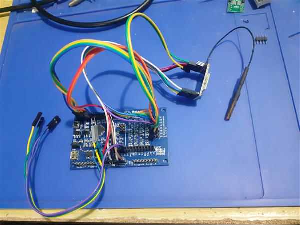
Basically something similar to the picture below:
In this picture, I have an existing RA-02 Breakout Module, with an 8 channel Logic converter and an Arduino Uno clone, along with all the needed wiring to make this setup possible… Quite a lot of wires indeed…
My solution:
I design and use quite a few LoRa PCBs and on all of them, I implement logic conversion using the BSS138 N-MOS Mosfet and 10k resistors. It is a cheap and reliable solution, but it can take up quite a lot of space on a PCB, as this means 11 Mosfets and 22 10k resistors if I were to provide level conversion to all of the RA-02’s GPIO and IO pins…
I also have the constant problem of many unnecessary wires, many of which sometimes fail straight out of the box, when prototyping something. I partly solved that by designing a few dedicated PCB solutions, but that is not always ideal,
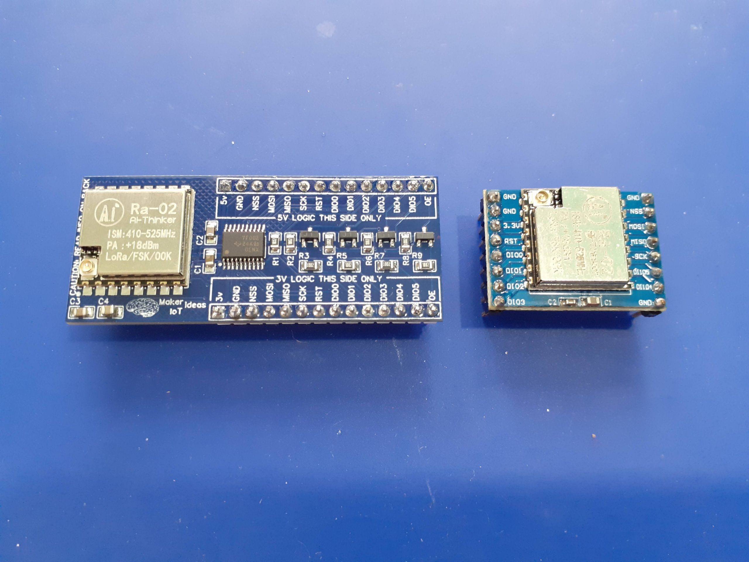
Using a dedicated Logic Converter IC, and Mosfet based converters to make up the difference, on a breadboard compatible module, seemed like a good idea, so I went ahead and designed the following solution:
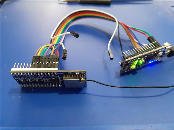
The breakout board module is breadboard compatible, and also has clearly marked pins to indicate the 3v and 5v sides of the module.
For my first test, I decided to test with an Arduino Uno Clone, since that is what most Makers and students will have access to. I used Cytron’s Maker Uno platform, which is equipped with some added goodies, in the form of diagnostic LED etc to make prototyping a lot easier.
As we can clearly see, It is only necessary to connect to the 5v logic side of the module, as well as provide 3v and 5v + GND to the module
In this test, I used Sandeep Mistry’s LoRa Library, with the Arduino IDE to do a quick test sketch.
As we can see, you need quite a lot more wires to make this work. It is also worth noting that we have only 8 level converters on this ATMEGA328P PCB, in order to use all of the RA-02’s GPIO, we will need to add an additional external logic converter as well.
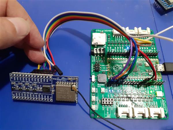
For my second test, I decided to be a bit brave, and try to use the new Raspberry Pi Pico ( RP2040 Microprocessor ). I have quite a few of them lying around and have never really done a lot with them, due to the fact that I do not really like using MicroPython or CircuitPython, and also because the recently released Arduino Core for the RP2040 still being quite new… I decided to use a development board that I recently bought from Cytron, the Maker Nano RP2040, as it has all the added diagnostic features to make my life a bit easier, I will also include a test with an original Pi Pico board, to make it more accessible to everyone out there.
Once again, I used Sandeep Mistry’s LoRa Library, with the exact same Arduino sketch, used for the Maker Uno test. (I obviously needed to change the pin numbers though, as the RP2040 uses different pins for its SPI interface).
Maker Nano RP2040 RA-02 Breakout Module
NSS 17
MOSI 19
MISO 16
SCK 18
RST 9
DIO0 8
In this case, we DO NOT need the OE pin, as the RP2040 is a native 3v device. The level converter can thus stay disabled, with its pins in tri-state ( high impedance ) mode.
If we look at the code, it is similar to the Maker Uno’s code, with only the Pin declarations needing a change
#include <SPI.h> // include libraries
#include <LoRa.h>
const int csPin = 17; // LoRa radio chip select
const int resetPin = 9; // LoRa radio reset
const int irqPin = 8; // change for your board; must be a hardware interrupt pin
byte msgCount = 0; // count of outgoing messages
int interval = 2000; // interval between sends
long lastSendTime = 0; // time of last packet send
// Note that SPI has different names on the RP2040, and it has 2 SPI ports. We used port 0
// CIPO (Miso) is on pin 16
// COPI (Mosi) is on pin 19
// SCK is on pin 18
// CE/SS is on pin 17, as already declared above
I did not use a breadboard, in order to make things as easy as possible.
To make things a bit easier, without having to resort to using a breadboard, I decided to do the Original Pi Pico test using the Maker Pi Pico PCB. This PCB is basically a big breakout module, with detailed pin numbers and some diagnostic LEDs, but it also uses a native Pi Pico, soldered directly to the PCB, by means of the castellated holes… So, While technically not being a true standalone Pico, It makes my life easier and was thus used for the test, as I can be sure that the pins are labelled exactly the same as on the original Pico.
The code used for the Maker Nano RP2040 works perfectly, with no changes required.
This post is getting quite long by now, so I have decided not to include my tests of the ESP-12E ( NodeMCU ) or ESP32 development boards here as well… They also function as expected.
In Summary
When I started this project, I set out to solve a problem ( personal to me ), that could potentially help a lot of other people use the RA-02 Module for more projects and tasks. The Breakout module in its current form can also be used with the RA-01h module (915Mhz Module) without any changes. All GPIO pins are broken out, and accessible through full logic converted pins on both sides of the breakout module.
I hope that this will be useful to someone. I am also not releasing the full schematics at this stage, as I may decide to make some minor cosmetic changes in the near future.
The PCB can however be ordered from PCBWay in its current form and works 100% as expected. The BOM file is available with the ordered PCB as usual.
This PCB was manufactured at PCBWAY. The Gerber files and BOM, as well as all the schematics, will soon be available as a shared project on their website. If you would like to have PCBWAY manufacture one of your own, designs, or even this particular PCB, you need to do the following… 1) Click on this link 2) Create an account if you have not already got one of your own. If you use the link above, you will also instantly receive a $5USD coupon, which you can use on your first or any other order later. (Disclaimer: I will earn a small referral fee from PCBWay. This referral fee will not affect the cost of your order, nor will you pay any part thereof.) 3) Once you have gone to their website, and created an account, or login with your existing account,
4) Click on PCB Instant Quote
5) If you do not have any very special requirements for your PCB, click on Quick-order PCB
6) Click on Add Gerber File, and select your Gerber file(s) from your computer. Most of your PCB details will now be automatically selected, leaving you to only select the solder mask and silk-screen colour, as well as to remove the order number or not. You can of course fine-tune everything exactly as you want as well.
7) You can also select whether you want an SMD stencil, or have the board assembled after manufacturing. Please note that the assembly service, as well as the cost of your components, ARE NOT included in the initial quoted price. ( The quote will update depending on what options you select ).
8) When you are happy with the options that you have selected, you can click on the Save to Cart Button. From here on, you can go to the top of the screen, click on Cart, make any payment(s) or use any coupons that you have in your account.
Then just sit back and wait for your new PCB to be delivered to your door via the shipping company that you have selected during checkout.
CAN-Bus allows us to add a lot of devices to a single bus (theoretically up to 127, with a practical limit of about 110). It was logical to decide to use CAN-BUS for communication between my LoRa-CAN Module and remote nodes in my ongoing farm telemetry system. In a previous project, I introduced the LoRa-CAN Gateway, which will be used to send/receive messages from the master control unit, the SX127x-RA-02-Module.
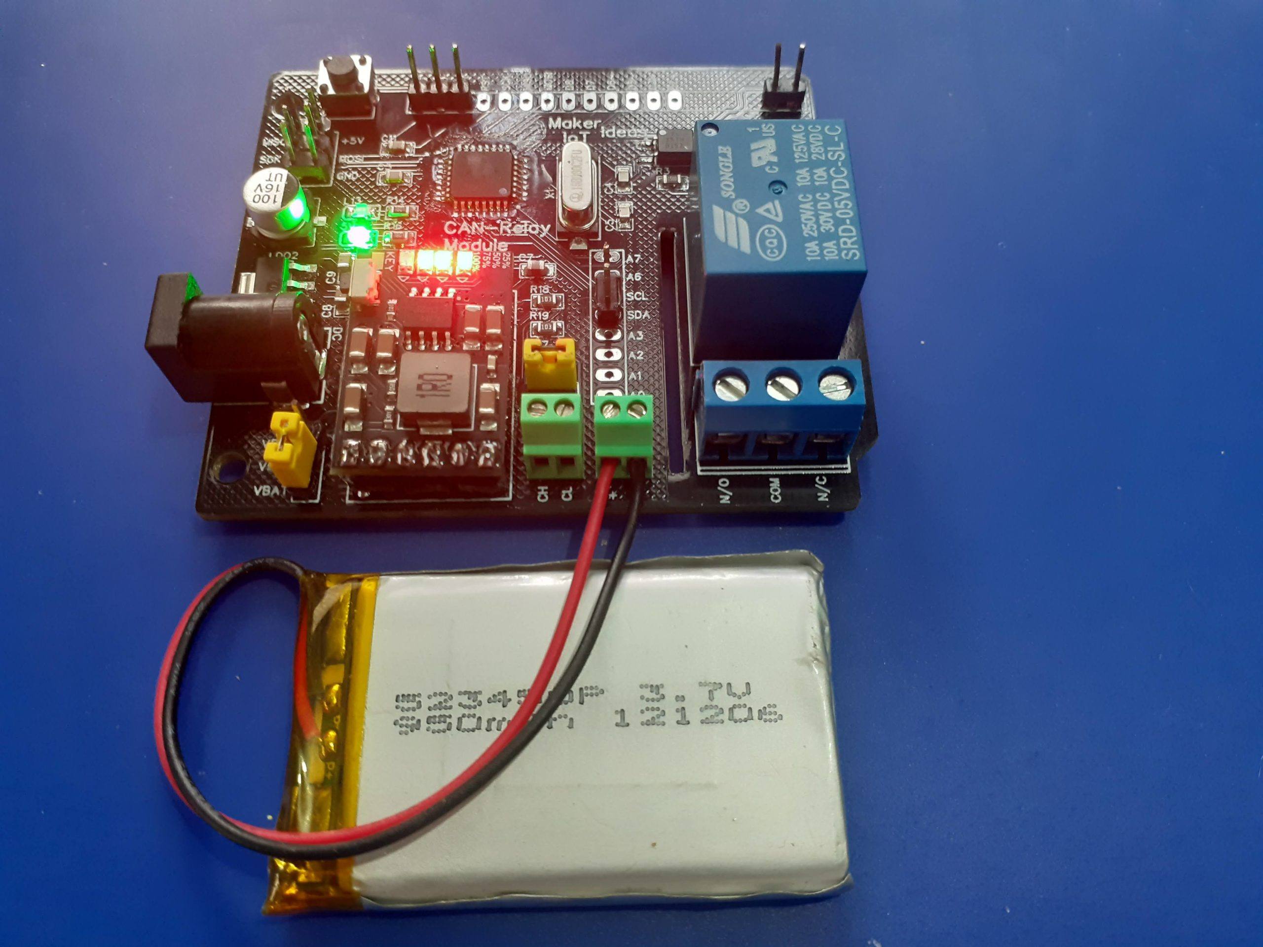
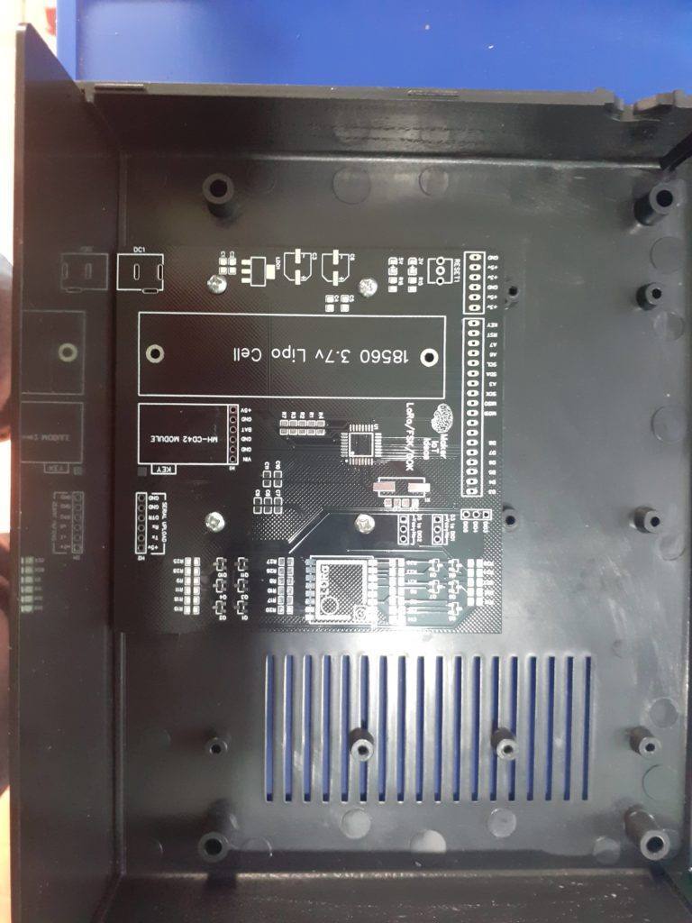
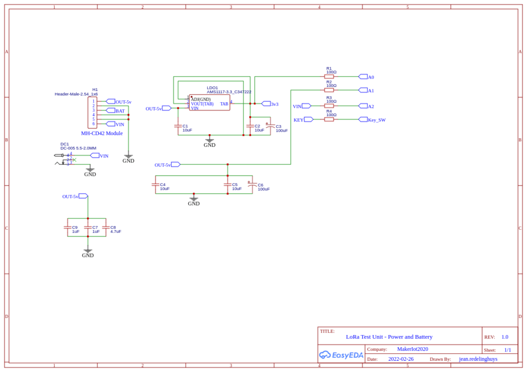
Today, I will focus on the design of the node device, an Arduino compatible CAN Relay Module PCB, with a built-in, CAN Controller and Transceiver ( MCP2515 and TJA1050 ), and the option to be powered from a LiPo battery (18650 or Single 3.7v Lipo cell), with charging provided by an MH-CD42 Module, similar to that used in the SX128x project mentioned above. The Module can also be powered directly from up to 12v DC by placing Jumper H2 in the V-REG position…
As mentioned in a previous project, the MH-CD42 module can provide up to 2A of current to charge a battery and provide 5V DC on a direct bypass circuit to power the rest of the circuit while the battery is being charged. This feature makes it ideal for my intended use, as I would only be needing battery power at night when the off-grid solar powered inverter is not actively charging the main batteries, and providing 220v AC.
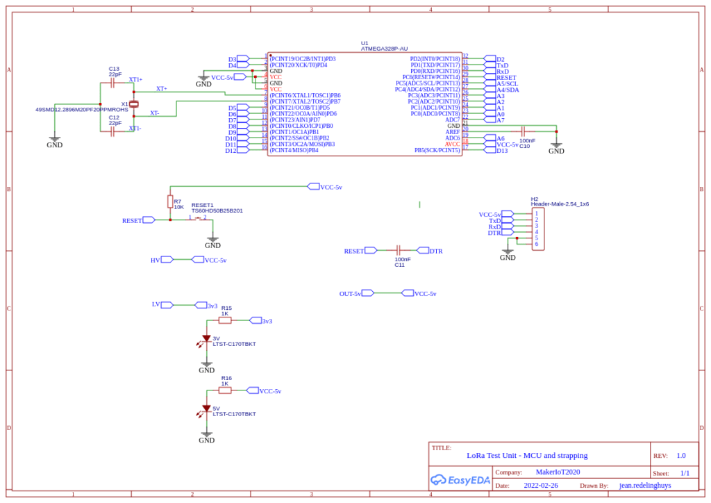
The CAN Relay Module PCB was designed to be as compact as possible, with a total footprint of the standard Arduino UNO. As space was at a premium, and to ensure that there are the absolute minimum additional components that will consume power when operating from the battery, I have not included any USB-to-Serial converters onboard. Firmware can be uploaded with an AVRASp, USBASP, Arduino as ISP or even an external USB-to-Serial converter ( providing that you load a bootloader into the Atmega Chip).
All of the unused GPIO pins on the ATMEGA chip is broken out into headers, with the exception of D10 ( which is used as CE/SS on the MCP2515 CAN controller), D9 which is connected to the Interrupt from the MCP2515, and D4, which is used to control the onboard Relay.
The MH-CD42 Module, and LiPo or 18650 Battery are completely optional, The device can function without these, by moving the H2 jumper to the VREG position as already mentioned above. This will divert the DC Voltage(Up to 12v) from the DC input adapter to the build-in 5v LDO voltage regulator to power the device.
If you place the H2 Jumper in the VBAT position, you need to install the MH-CD42 module to provide power to the rest of the PCB, as well as keep the LiPo battery or 18650 Cell charged…
Please NOTE:
When the MH-CD42 module is in use, the total DC input voltage through the DC input adapter SHOULD NOT exceed 5.5v DC! This is a limitation in the operating parameters of the MH-CD42 module. Not paying attention to this will result in damage to the MH-CD42 Module.
You could also power the module with REGULATED 5v DC, directly from any 5v header pin. Please note that in this case,
1) The battery won’t be charged.
2) The LDO regulator will not be in operation.
The Microcontroller
The CAN Relay Module can use any of the ATMEGA8a/88/168/328 AVR microcontrollers, as the pinout is identical. I believe this is an advantage, especially with the current chip prices, where my last quote for an ATMEGA328P-AU was 69$USD!!!! This is in comparison to the 4 to 5 USD each for an ATMEGA8a or ATMEGA168 ( We must also remember though that the 328p is very well known, and thus have higher demand. The 8a/88 or 168 are less well known, have much less memory and flash area, and will thus be cheaper. A word of action though, I had strange issues with I2C on the Atmega8a with Mini core, to such an extent that I2C does not work at all?
If you plan to use I2C on this board, install a 328p right from the start, and save yourself a lot of headaches!
This is the Relay driver circuit. As you can see, it is optically isolated, and active LOW. This means that you have to pull D4 LOW to energise the relay. Also note that, although the relay is optically isolated from the microcontroller, the coil is NOT galvanically ISOLATED. The load, which is magnetically switched, will be truly galvanically isolated, providing of course that you don’t do something silly like using a common ground to the PCB as a common on the relay…
This is the Processor and Power-supply schematic. The circuit is basically a standard Arduino Nano, with modifications for the CAN Controller on the next schematic page. Note that the MH-CD42 is not shown on the schematic. The VBAT net connects directly to the VIN pin on the unit, with the BAT net connecting to the positive of the battery. VOUt-5v from the module goes directly to the 5v net. All grounds are commoned.
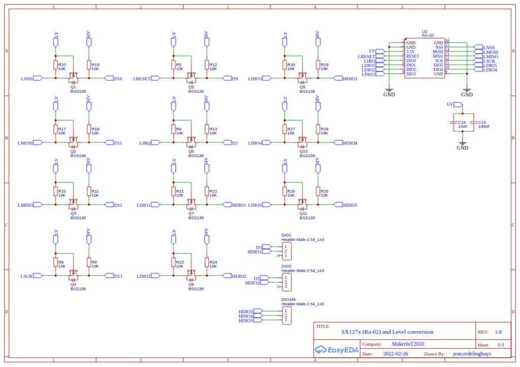
This is the CAN Controller and Transceiver circuitry. The MCP2515 connects directly to the SPI bus on the microcontroller via D13, D12 and D11, with D10 as CE/SS and D9 as Interrupt or IRQ. It is important to note that although the MCP2515 is a 3v capable device, the TJA1050 Can transceiver is 5v only. This prevents us from running the PCB at 3v unless, of course, we change the TJA1050 out for a 3v capable device…
As I am currently working on the final integration of the two modules, I am not yet ready to publish my final code, showing the operation between the CAN-Bus and LoRa-to-CAN Gateway device in this post. Once I am happy that all issues are definitively sorted out, I will publish my code.
This PCB was manufactured at PCBWAY. The Gerber files and BOM, as well as all the schematics, will soon be available as a shared project on their website. If you would like to have PCBWAY manufacture one of your own, designs, or even this particular PCB, you need to do the following… 1) Click on this link 2) Create an account if you have not already got one of your own. If you use the link above, you will also instantly receive a $5USD coupon, which you can use on your first or any other order later. (Disclaimer: I will earn a small referral fee from PCBWay. This referral fee will not affect the cost of your order, nor will you pay any part thereof.) 3) Once you have gone to their website, and created an account, or login with your existing account,
4) Click on PCB Instant Quote
5) If you do not have any very special requirements for your PCB, click on Quick-order PCB
6) Click on Add Gerber File, and select your Gerber file(s) from your computer. Most of your PCB details will now be automatically selected, leaving you to only select the solder mask and silk-screen colour, as well as to remove the order number or not. You can of course fine-tune everything exactly as you want as well.
7) You can also select whether you want an SMD stencil, or have the board assembled after manufacturing. Please note that the assembly service, as well as the cost of your components, ARE NOT included in the initial quoted price. ( The quote will update depending on what options you select ).
8) When you are happy with the options that you have selected, you can click on the Save to Cart Button. From here on, you can go to the top of the screen, click on Cart, make any payment(s) or use any coupons that you have in your account.
Then just sit back and wait for your new PCB to be delivered to your door via the shipping company that you have selected during checkout.
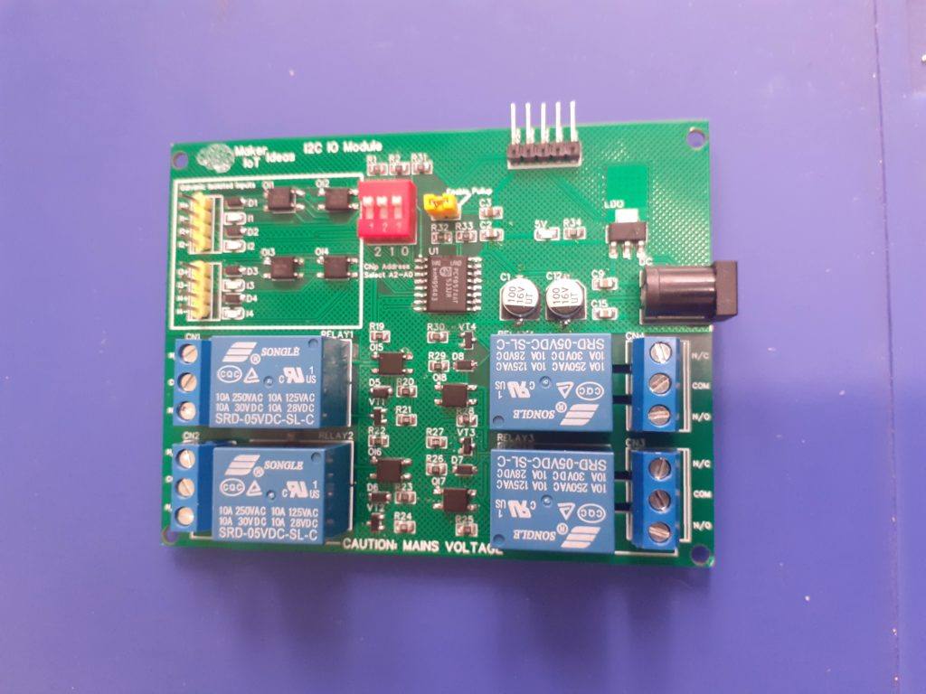
Sometimes we need extra Inputs or Outputs on a device, or for use with a project. To implement it properly we also need a lot of additional electronic components to properly isolate these inputs and outputs, with the signals they switch, from our own project, because, let us be real, electronics and electrical devices in the real world do not all work with Arduino or ESP32/ESP8266 save voltages ( 5v and 3.3v ).
I will also tell you about a very special deal to get PCBs of your own made for only one (1) USD ( Including shipping with DHL )! No, I am not joking, and I am not crazy either… More on that later in the post…
It is thus extremely important to have a module that can effectively interface with inputs of 5.5v up to 32v DC ( optically Isolated up to 3000v ), and relay outputs, also optically isolated at 3000v. ( Note that the optical isolation voltage does not mean you can input that voltage level into the chip! It means that it can isolate the electronics on the safe side of the isolator from a voltage spike of up to that voltage!).
I also love using I2C, as it allows me to add modules onto an existing data bus while using only 2 GPIO lines on the MCU!
The module I am presenting to you today was designed to be operated from 5v DC. That includes the I2C data lines (SDA and SCL). If you need to interface to a 3.3v microprocessor, like an ESP32 or ESP8266, or even the new RP2040 or an STM32, you need to use a logic level converter.
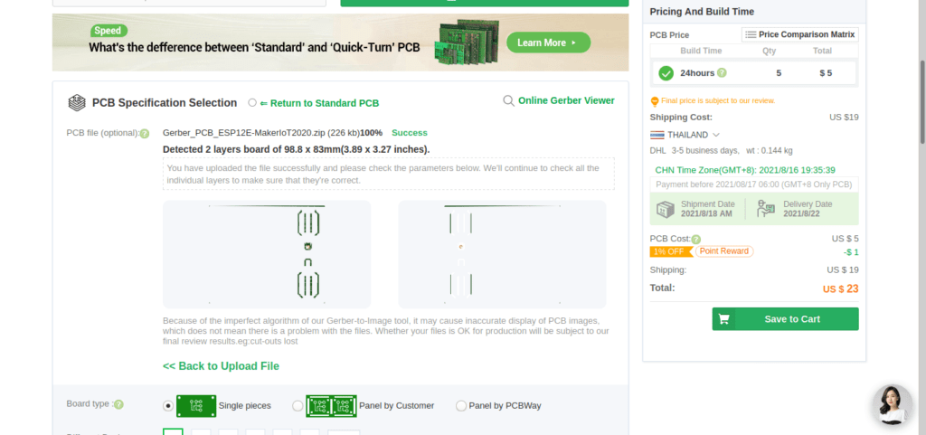
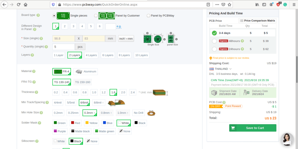
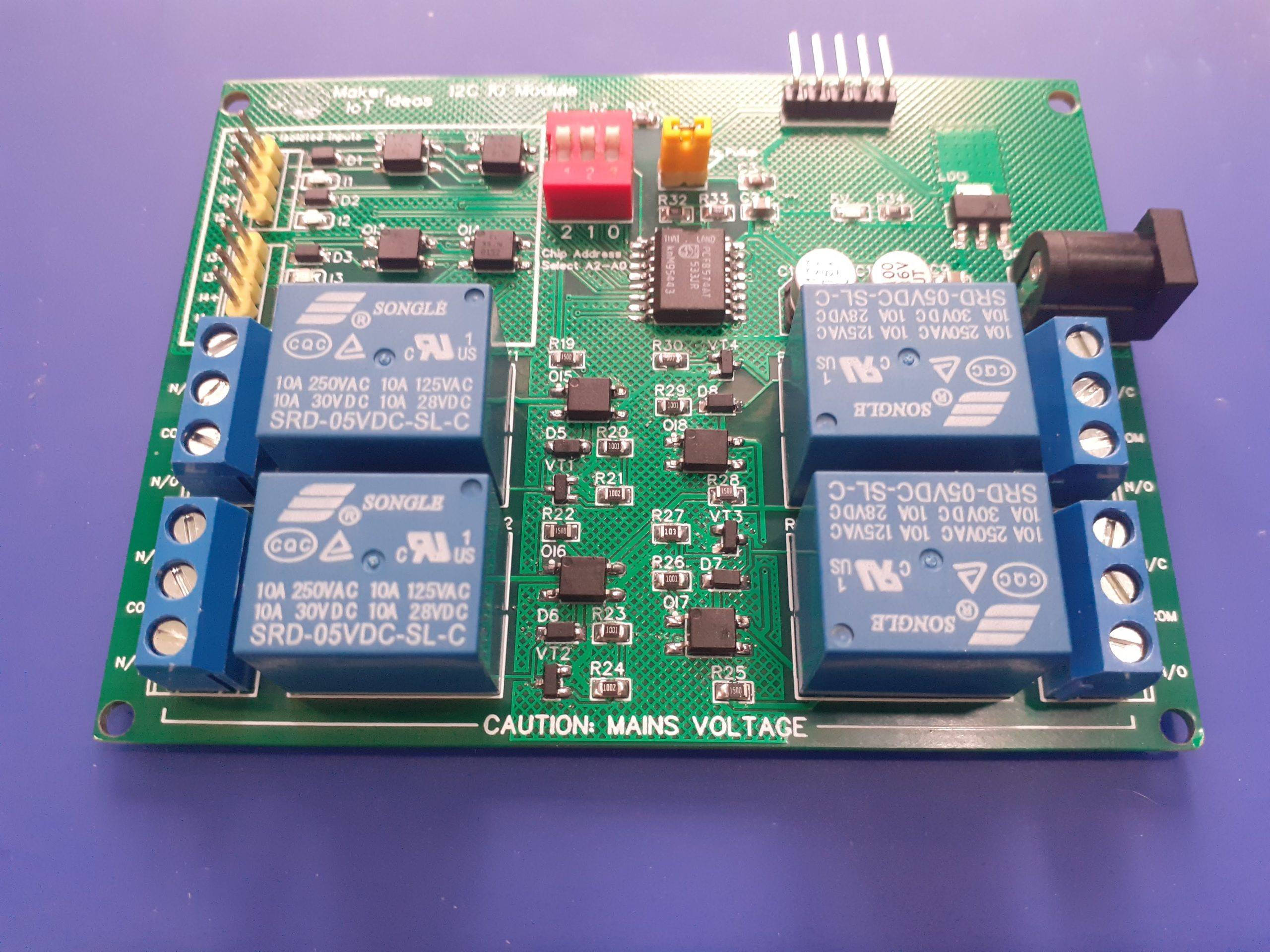
The PCB uses the popular PCF8574 8 channel IO expander, which is extremely easy to use, and where you can connect up to 8 devices in a chain ( 16 if you use the PCF8574AT variant as well.. Meaning eight of each variant) This surely adds up to quite a lot of IO lines at a cost of only 2 GPIO on your MCU!
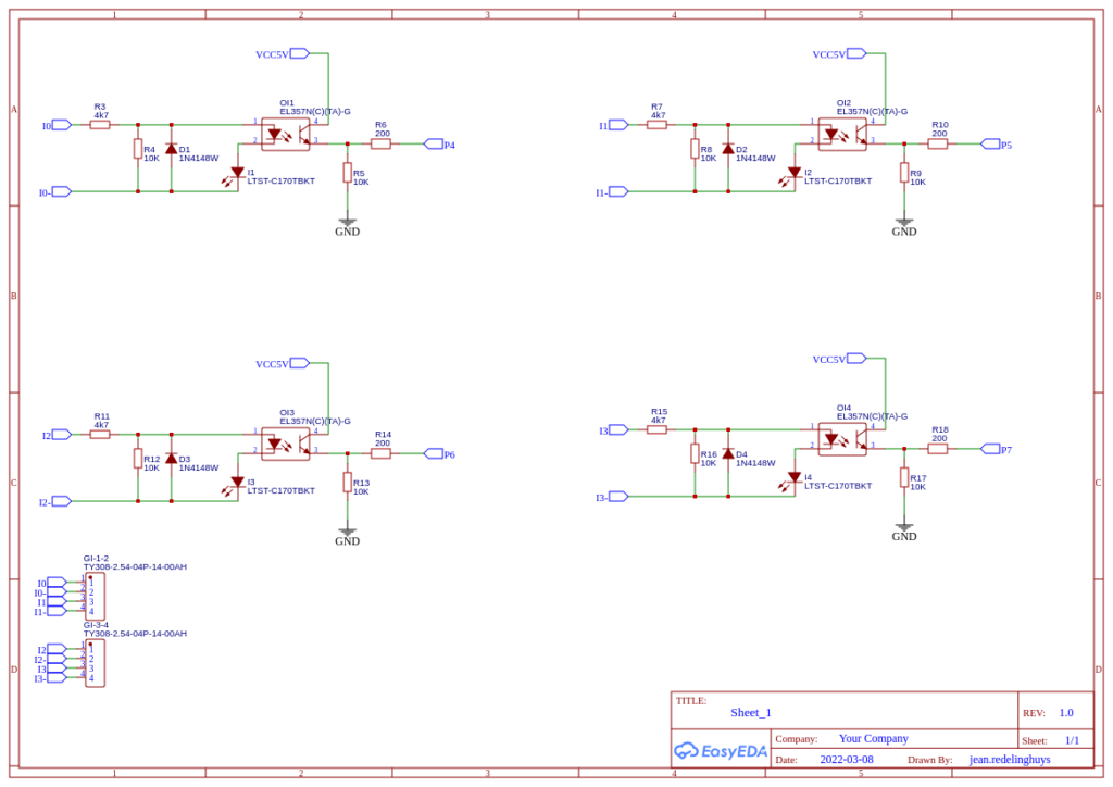
The Circuit diagram is below, and I will discuss each part briefly.
Schematic – Page 1
This is the Galvanic Isolated Input schematic. Each input operates at a voltage of 5.5v to 32v DC. Complete Galvanic Isolation between the Module and the remote input is in effect. Please note that you have to supply a remote ground from the device that provides the input. DO NOT connect the PCB Module ground to an isolated ground pin. This may still work but renders the galvanic Isolation for that input completely useless.
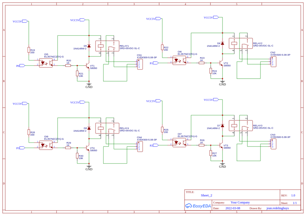
Relay Driver Schematic
This is the Relay driver schematic. Each relay output is driven through an optocoupler, as well as a transistor. Although this arrangement does not provide complete galvanic Isolation of the relay coil, it does protect your MCU from any voltage spikes caused by back-emf when the relay is de-energised. The Relay contacts themselves, being magnetically actuated by the coil, are in themselves Galvanically Isolated from the rest of the PCB.
I2C Control Schematic
Finally, we have the I2C IO Expander schematic, with a 5v LDO regulator, capable of providing up to 600mA of current to the PCB. The PCF8574 Chip’s address is selectable with DipSwitch SW1 so that you can use multiple PCBs at the same time if you should choose to do so. The only note on that is that you should not connect the 5v lines of each individual PCB together. You should also only connect the GND and SDA, SCL lines back to the MCU.
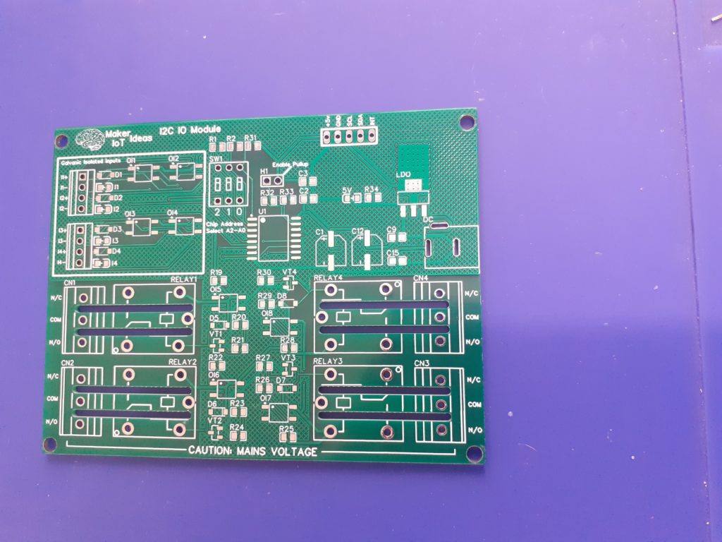
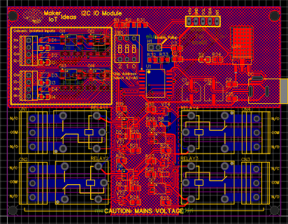
Raw PCB Layout
Earlier on in the post, I promised to tell you about a very special deal…
Well, here it is, as well as some details about the sponsor of this very exciting deal…
PCBPartner.com is owned and operated by Kinji Group, which was established in 1997. We have over 20 years of experience in PCB manufacturing, PCB design, component manufacturing and distribution, PCB assembly and PCB cam software development.
While Kinji Group has 3 PCB factories in China, we have also developed strategic partnerships with more than 15 other factories around Asia. We, therefore, have a large group of specialists in PCB manufacturing, quality control, technical support and part sourcing to support your innovative ideas and products.
Our over 500 employees are spread across 8 branches in Mainland China (Shenzhen, Dongguan, Shanghai, Wuxi, Chengdu, Xiamen), Hong Kong SAR, and Taiwan. And we’re still growing!
We’re confident once you try us out, we’ll become your PCB Partner. And if not? Well, you’ll have scored some free PCB! So why not take us for a spin, you’ve got nothing to lose.
We, MakerIoT2020.com, have decided to give it a go and send this particular PCB to PCBPartner.com for manufacturing. So far, while we are still waiting to receive the PCB, ( Weekends happen 🙂 ), We are very happy with the ease of use of the online ordering system provided.
We would also like to point out that this special order will only be available until the end of March 2022, as well as that there are a few conditions:
Promotion ends March 31st 2022 Each new customer can enjoy free PCB on their first order This promotion applies to 1-2 layers of FR4 PCB, up to 100x100mm, 10pcs, with Green Solder Mask 4 layer of FR4 PCB, up to 50x50mm, 10pcs, with Green Solder Mask 1 layer Aluminum PCB, up to 100x100mm, 10pcs This PCB promotion cannot be used with other discounts or other promotional activities
For a full list of conditions, and countries that may participate in this offer, please click on the link here
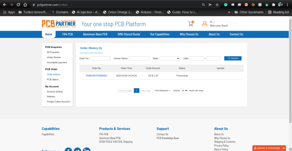
Let us have a look at the entire ordering process..
Once you click on the PCBPartner.com link, you will be taken to their website, where you should sign up, which is free and easy… We used our Google.com account details and were ready to order in seconds…
FR4 PBC Quote Form – Before uploading your Gerber Files
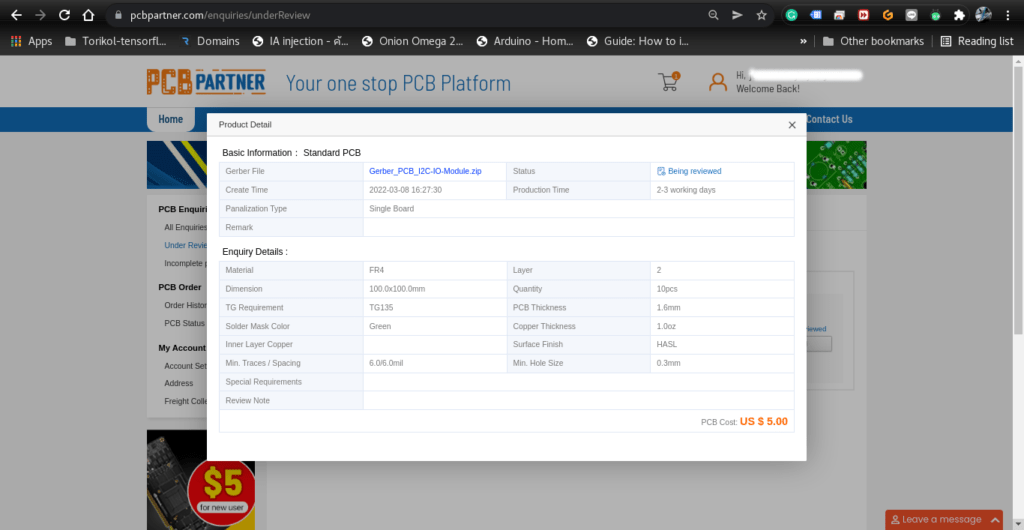
Enter the specific details for the manufacturing of your PCB, and upload your Gerber files.
After uploading your Gerber Files.
Continue selecting options for your PCB order… Make sure to select DHL shipping, to take advantage of the special 1USD option, and click on the ADD to Cart Button…
Quote added to your shopping cart.
You will now get a message that your enquiry has been submitted successfully.
Click on the “Under review” button, to see your quote status… In my case, it took about 5 minutes for the review to pass, and be able to checkout and pay for the order…
PCB order under review
Once the review has passed, you will see a pending payment,
Payment Pending
You may now click on the “Proceed to Payment” option
Add your shipping address, and choose your payment option.
At this moment in time, only two payment options are supported, Paypal ( as well as Debit and Credit cards) and Direct Bank Transfer. I believe more options will be made available in future.. Checkout with Paypal
In my case, I chose Paypal and paid by Debit card.
Enter your card detailsAfter Payment.
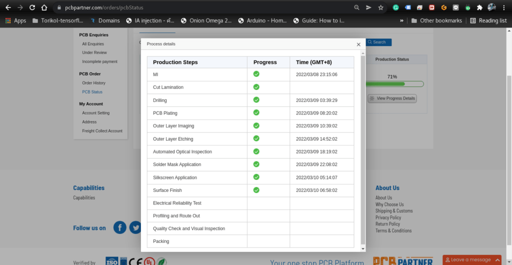
After payment was made successfully, you can also check on the status of your order…
Review your order status
You can also review your order at any stage before or after payment, as well as get progress reports of the manufacturing process.
PCB Order Status.
In conclusion, I would like to say that it was quite easy to order and make payment. The Website is easy to use, and everything is clear and easy to understand. The PCB was well manufactured and seems to be quite good quality
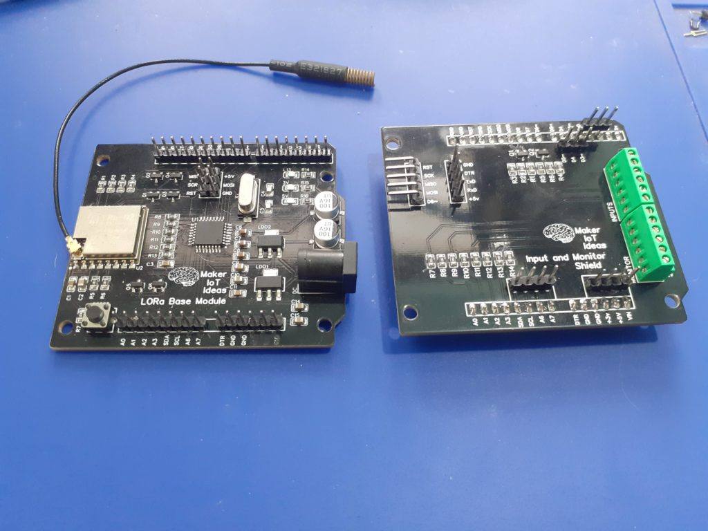
This is a straightforward project compared to my usual PCB projects. It is one of a series of designs towards completing my LoRa monitoring system, that I plan to use on the farm to monitor various areas, such as intrusion detection, battery levels etc.
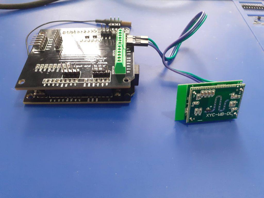
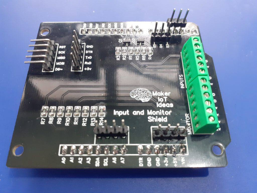
The shield was designed to fit on top of the first LoRa Base Module. It was designed to allow easy, neat connections to Infrared Beam sensors, XYC-WB-DC Motion Detector, as well as to monitor the battery levels at the Solar power inverter (the farm is completely off-grid).
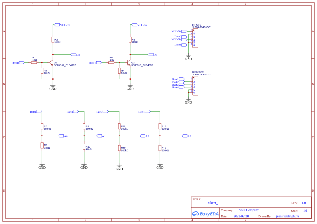
The Motion Sensor provides a +3v signal that goes high on motion detection, while the Infrared Beam Sensor provides a relay contact that can be used to provide a similar voltage signal. As I prefer to use pull-up logic on my inputs, I decided to implement a simple transistor circuit where the input will switch the base of the transistor, which in turn will pull the input to signal ground when switched on. This circuit uses the S8050 transistor, with the base pulled down to signal ground via a 10k resistor to prevent floating, and a current limiting resistor of 1k to 1k8 on the base. The collector, as well as the D7 and D8 GPIO pins on the LoRa Base Module, is pulled High to Vcc5v via a 10k resistor.
Voltage monitoring is done with the ADC on the LoRa Base Module, with each of the 4 battery levels ( 12v, 24v,36v, and 56v) being connected to the relevant ADC channel via a resister-divider network to lower the respective voltage to a level between 0 and 5v. ( This was done as the ADC on the ATMEGA328p can only handle a maximum voltage of 5.0v )
The resistors were chosen to give a slightly bigger input voltage range, to accommodate for fluctuations from the solar charger ( It can sometimes go up to 65v on a very bright sunny day ). I decided to not add any current limiting resistors directly onto the PCB, as they are definitely going to be bulky. They will instead be attached externally, to suitable heatsinks, etc…
As this PBC is still in the prototype stage, and my LoRa Monitoring device will definitely go through quite a few modifications in future, I provided access to all unused GPIO pins via separate headers on the shield. Most notably the SPI Header, used for programming the ATMEGA328P MCU, or connecting other SPI devices ( I am working on a CAN bus addon for the device, to save on the number of physical radio nodes that needs to be installed), The UART Header, as well as I2C, A6, A7 and additional Digital IO Pins (D3~, D4, D5~).
In the photo above you will notice an additional header on the UART pins, This was added to assist me with debugging on the logic analyser, as I had a slight issue with waking up the ATMEGA328P, and getting it to send events via LoRa. It would wake up, print status messages through the UART, but never do the actual LoRa part! That has now been fixed, and the header removed…
The schematic diagram for the shield is below. As you will see, it is very uncomplicated indeed.
The RA-02 Module (SX1278) connections to the ATMEGA328p is as follows:
NSS to D10 (CE)
MOSI to D11 (MOSI)
MISO to D12 (MISO)
SCK to D13 (SCK)
RESET to D9
DIO0 to D2 ( We need a hardware Interrupt pin ).
DIO1 to DIO5 was not broken out on the current version of the LoRa Base Module
There is also no direct access to pins D10, D9 and D2 either on the LoRa Base Module or on the Input and Monitor Shield.
If you do decide to hack the device and add access to any of the non broken out pins, please remember to use a logic level converter between the ATMEGA328 and the SX1278, as they operate at different voltages, and the SX1278 is not 5v tolerant on any of the IO Pins!
You can order this shield from PCBWay by clicking here
This PCB was manufactured at PCBWAY. The Gerber files and BOM, as well as all the schematics, will soon be available as a shared project on their website. If you would like to have PCBWAY manufacture one of your own, designs, or even this particular PCB, you need to do the following… 1) Click on this link 2) Create an account if you have not already got one of your own. If you use the link above, you will also instantly receive a $5USD coupon, which you can use on your first or any other order later. (Disclaimer: I will earn a small referral fee from PCBWay. This referral fee will not affect the cost of your order, nor will you pay any part thereof.) 3) Once you have gone to their website, and created an account, or login with your existing account,
4) Click on PCB Instant Quote
5) If you do not have any very special requirements for your PCB, click on Quick-order PCB
6) Click on Add Gerber File, and select your Gerber file(s) from your computer. Most of your PCB details will now be automatically selected, leaving you to only select the solder mask and silk-screen colour, as well as to remove the order number or not. You can of course fine-tune everything exactly as you want as well.
7) You can also select whether you want an SMD stencil, or have the board assembled after manufacturing. Please note that the assembly service, as well as the cost of your components, ARE NOT included in the initial quoted price. ( The quote will update depending on what options you select ).
8) When you are happy with the options that you have selected, you can click on the Save to Cart Button. From here on, you can go to the top of the screen, click on Cart, make any payment(s) or use any coupons that you have in your account.
Then just sit back and wait for your new PCB to be delivered to your door via the shipping company that you have selected during checkout.
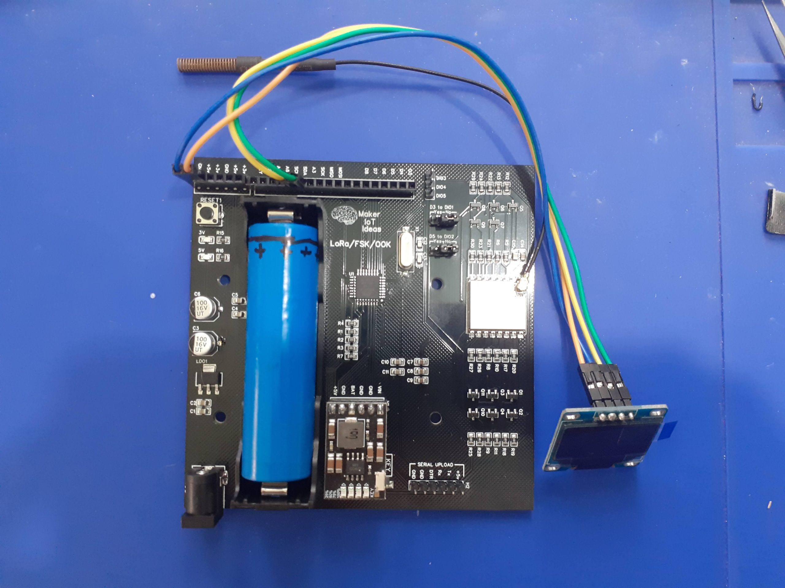
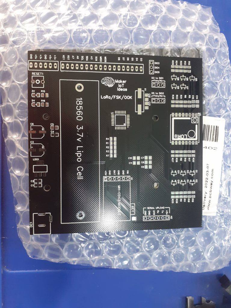
SX127x LoRa/FSK/OOK Module with LiPo battery-backup
SX127x LoRa/FSK/OOK Prototype Radio Board
I recently had a requirement to do some automation/telemetry on the farm. Things went missing, unauthorised persons were trespassing on the property, helping themselves to eggs, chickens, ducks and produce. Something had to be done, and as there is nobody sleeping there at night, it had to be possible to get remote status updates in real-time.
The farm is also completely off-grid, with solar-powered inverters taking care of all the water and electricity needs. Power usage monitoring could thus be a great help as well…
The idea is as follows:
Have a central control station, with various remote devices to do intrusion detection, control lights and water pumps, as well as monitor the battery levels of the inverter and solar-panel system. As the area is quite large, having to pull in electrical cabling will not be feasible, nor could the inverter handle all of that.
I decided to use the RA-02 LoRa/FSK/OOK module, on a custom PCB, but with various different PCB modifications, to take care of each stage of the project. The PCB that I will present today will be mainly used as the control unit, but it could also be a remote station, depending on what options are needed.
The ATMEGA328P-AU MCU is used as the main processor on each board, with the MH-CD42 Boost Converter/LiPo battery charger module taking care of power supply requirements. This module can source up to 2A at 5.0v, More than adequate for my needs. The ATMEGA328P will be put into sleep mode, to wake on interrupt to respond to events as needed ( To help save power ). Power usage of the circuit is around 50mA in standby ( NOT SLEEP MODE ), and with a peak of 100mA on a LoRa Transmit or Receive event.
The RA-02 Module did however present some challenges, as it is a 3.3v device, with non-5v capable IO lines. This made it necessary to include a 3.3v LDO regulator, as well as logic level converting circuitry onto the PCB. To allow for the most flexibility, all DIOs on the RA-02 was also broken out via level converters, in addition to the required SPI pins ( MOSI, MISO, CE and SCK ). This amount to a total of 11 level converters onboard.
I chose the MH-CD42 Power module for the reason that it can supply current at the same time as charging the LiPo battery (in my case, I used a 18650 cell). This will help greatly, as 220v inverter power is available during the day to charge the batteries.
Another challenge was definitely the enclosure. I found some really nice enclosures online, but the mounting holes were located in a very particular pattern, making it necessary to do some very careful measuring to get the PCB to fit exactly. The enclosure also has space to accept the other PCB modules, like the USER Control panel, and other sensor devices as needed. PCBWay did a great job at manufacturing the PCB so as to fit exactly. I must admit that I had quite a few tense moments between sending the PCB off to manufacturing and receiving it, as to whether my measurements were actually accurate, and if the PCB would fit as I imagined…
As you can see in the picture above, it turned out perfectly.
The Circuit diagram is basically a standard Arduino Nano ( I needed access to all of the ADC pins ),
Connections to the RA-02 module is as follows:
RA-02
ATMEGA328P
MOSI
D11
MISO
D12
SCK
D13
CE
D10
RESET
D9
DIO0
D2 ( We need a hardware interrupt pin here )
DIO1
D3 ( Hardware Interrupt, enabled through jumper)
DIO2
D5 ( Enabled through a jumper)
DIO3 to DIO 5
Not connected, available on a breakout header
Connections between Ra-02 (SX127x) and ATMEGA328P – Note that all IO Lines are connected through level converters 5v <-> 3.3v
On the ATMEGA328, the following pins are broken out into headers:
D3
can be connected to RA-02 with a jumper
D4
D5
can be connected to RA-02 with a jumper
D6
D7
D8
D13 ( SCK )
Broken out as a 5v logic pin
D12 ( MISO )
5v logic pin
D11 ( MOSI )
5v logic pin
A3,A6,A7
ADC Pins ( A0, A1, A2 is used internally to monitor VIN, VCC5v and VCC3v ) A0 = Vcc3v A1 = Vcc5v A2 = VIN
SCL
I2C SCL pin OR A5 (I2C pins are at 5v logic levels )
SDA
I2C SDA pin OR A4 (I2C pins are at 5v logic levels )
RESET
DTR
( connected through a 100nf Cap to Reset, used for serial uploading firmware )
D0 ( RxD )
UART Rx Pin ( 5v logic )
D1 ( TxD )
UART Tx Pin ( 5v logic )
ATMEGA328P breakout pins. All pins are at 5v logic level
The ATMEGA328P is clocked at 16Mhz through an external crystal.
3v, 5v and GND pins were broken out at two opposite corners of the PCB to allow easy connection of additional devices/ sensors as needed.
The MH-CD42 module has the capability to power a load while charging the LiPo battery. This makes it possible to do a few interesting things while supplying power to this particular PCB.
The board can be powered directly from a 5v header pin ( NOT from the DC1 input ). In this mode, a LiPo battery is not required.
5v will be directly supplied to the processor, as well as the 3.3v LDO regulator, allowing the RA-02 module to function as well.
PLEASE NOTE: THERE ARE NO 5v REGULATION – MAKE SURE YOU SUPPLY REGULATED 5v
Installing the MH-CD42 module will add the option of charging a 3.3v 18650 Lipo battery, as well as powering the board at the same time. You need to supply power through the DC plug to make use of this function. This mode is also a miniature uninterruptible power supply, with the 3.3v LiPo battery immediately taking over should the main DC input fail.
NOTE: The MH-CD42 can only accept up to 5.5v MAXIMUM as input!
Software:
The PCB can be used with LoRa libraries from Sandeep Mistry OR JGromes/RadioLib ( If you want to do FSK/OOK or other advanced stuff like LoRa of FHSS)
Both libraries have extensive examples showing how to use them. As our use case will definitely differ, I will not have any example here at this stage. I will add one later after the entire project is completed, with all the relevant modules.
This PCB was manufactured at PCBWAY. The Gerber files and BOM, as well as all the schematics, will soon be available as a shared project on their website. If you would like to have PCBWAY manufacture one of your own, designs, or even this particular PCB, you need to do the following… 1) Click on this link 2) Create an account if you have not already got one of your own. If you use the link above, you will also instantly receive a $5USD coupon, which you can use on your first or any other order later. (Disclaimer: I will earn a small referral fee from PCBWay. This referral fee will not affect the cost of your order, nor will you pay any part thereof.) 3) Once you have gone to their website, and created an account, or login with your existing account,
4) Click on PCB Instant Quote
5) If you do not have any very special requirements for your PCB, click on Quick-order PCB
6) Click on Add Gerber File, and select your Gerber file(s) from your computer. Most of your PCB details will now be automatically selected, leaving you to only select the solder mask and silk-screen colour, as well as to remove the order number or not. You can of course fine-tune everything exactly as you want as well.
7) You can also select whether you want an SMD stencil, or have the board assembled after manufacturing. Please note that the assembly service, as well as the cost of your components, ARE NOT included in the initial quoted price. ( The quote will update depending on what options you select ).
8) When you are happy with the options that you have selected, you can click on the Save to Cart Button. From here on, you can go to the top of the screen, click on Cart, make any payment(s) or use any coupons that you have in your account.
Then just sit back and wait for your new PCB to be delivered to your door via the shipping company that you have selected during checkout.
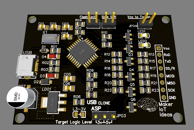
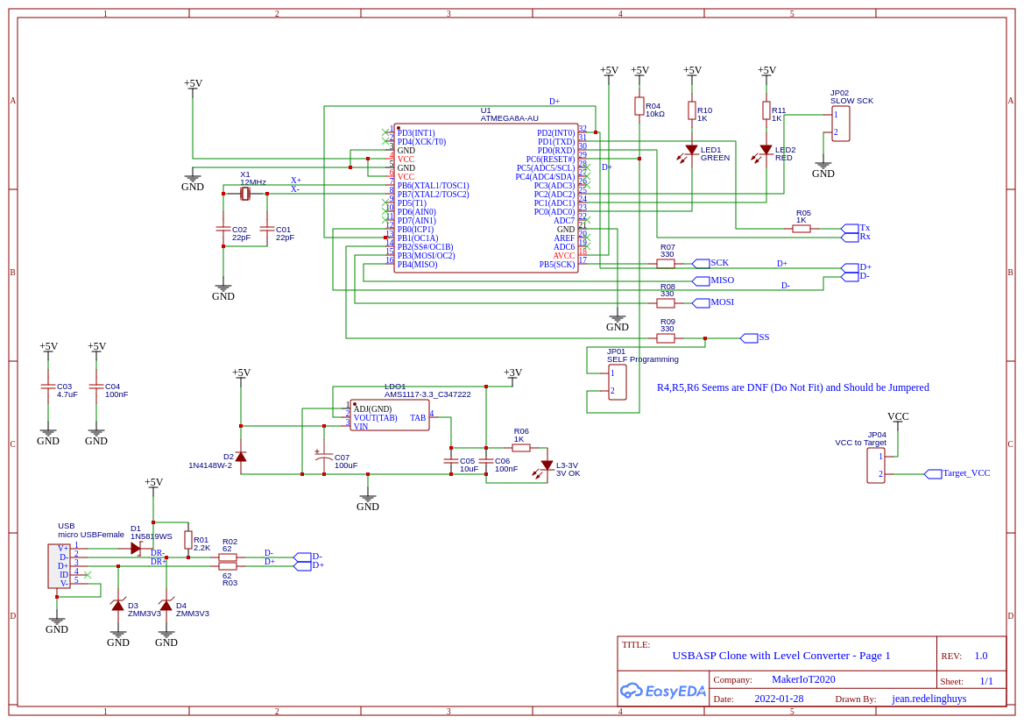
Using more ATMEGA based MCU’s in my recent projects, and not using ready-made Arduino boards for any of them, it became necessary to invest in a dedicated ASP programmer to flash the MCU’s. Huge delays on electronics components, with confirmed orders being mysteriously cancelled due to sourcing issues, and the high cost of “original OEM ASP programmers”, send me on a search for a DIY style programmer, like the old “NOPPP” ( NO PARTS PIC Programmer) in the good old days…
Personal computers have changed a lot, and while ATMEGA chips are not PIC’s, I did feel that it could be done. Given the fact that you could also use an Arduino UNO as an ISP, and doing a little more digging, I finally found a very attractive alternative…
Thomas Fischl, on his website,https://www.fischl.de/usbasp, has an open-source hardware project, that seemed to be exactly what I needed. His device is capable of programming 5v devices, at various speeds, including a super slow one. He has also written firmware for the device, and although the last update was in 2011, It still seems to be working well, or at least as far as I can see…
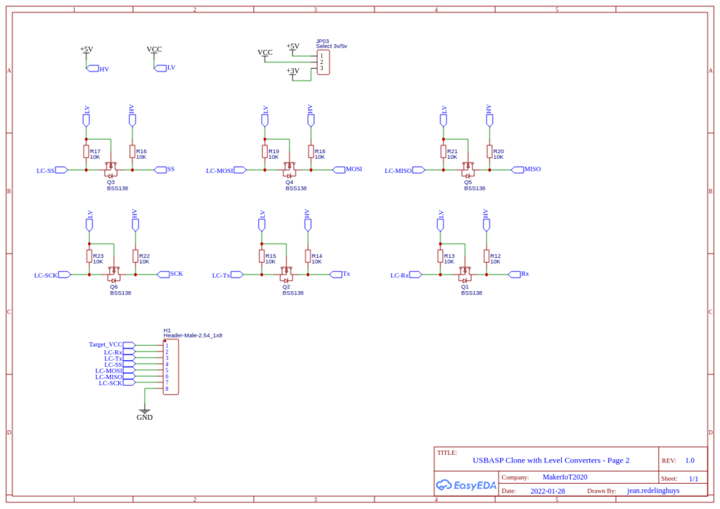
I did however decide to add my own twist to the design and build in a logic level converter, to be able to program 3.3v devices as well…
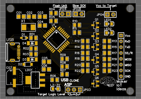
The modified schematic is below:
Schematic Page 1Schematic Page 2
I chose to do my own PCB layout, to incorporate the changes listed earlier, namely the logic level conversion from 5v to 3v, as well as adding a 3.3v LDO voltage regulator to provide 3.3v to the target in case it is required.
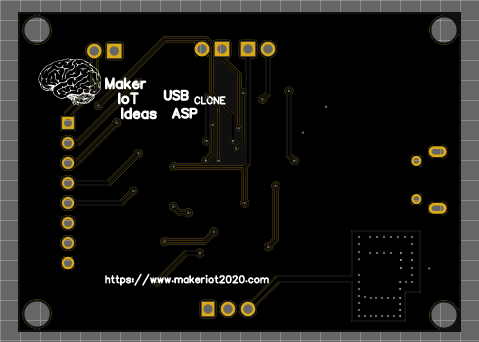
PCB TopsidePCB Bottom Side3D Render of the PCB
The PCB is still in transit from the factory, and thus I will update this article later with pictures of the actual device.
Firmware can be flashed using any ASP programmer, Arduino as ISP as well, but with the caveat that you have to use AVRDude from the command line… More on that in the follow-up post… ( I would like to show actual screenshots of the process, and not theory.. ). The links to the firmware are available on https://www.fischl.de/usbasp, courtesy of Thomas Fischl, whom I would like to thank for making this open-source hardware project available freely, as well as for writing and maintaining the firmware.
The PCB can be ordered, or the design files downloaded ( a free download ) from my Projects page at PCBWay soon…
This PCB was manufactured at PCBWAY. The Gerber files and BOM, as well as all the schematics, will soon be available as a shared project on their website. If you would like to have PCBWAY manufacture one of your own, designs, or even this particular PCB, you need to do the following… 1) Click on this link 2) Create an account if you have not already got one of your own. If you use the link above, you will also instantly receive a $5USD coupon, which you can use on your first or any other order later. (Disclaimer: I will earn a small referral fee from PCBWay. This referral fee will not affect the cost of your order, nor will you pay any part thereof.) 3) Once you have gone to their website, and created an account, or login with your existing account,
4) Click on PCB Instant Quote
5) If you do not have any very special requirements for your PCB, click on Quick-order PCB
6) Click on Add Gerber File, and select your Gerber file(s) from your computer. Most of your PCB details will now be automatically selected, leaving you to only select the solder mask and silk-screen colour, as well as to remove the order number or not. You can of course fine-tune everything exactly as you want as well.
7) You can also select whether you want an SMD stencil, or have the board assembled after manufacturing. Please note that the assembly service, as well as the cost of your components, ARE NOT included in the initial quoted price. ( The quote will update depending on what options you select ).
8) When you are happy with the options that you have selected, you can click on the Save to Cart Button. From here on, you can go to the top of the screen, click on Cart, make any payment(s) or use any coupons that you have in your account.
Then just sit back and wait for your new PCB to be delivered to your door via the shipping company that you have selected during checkout.
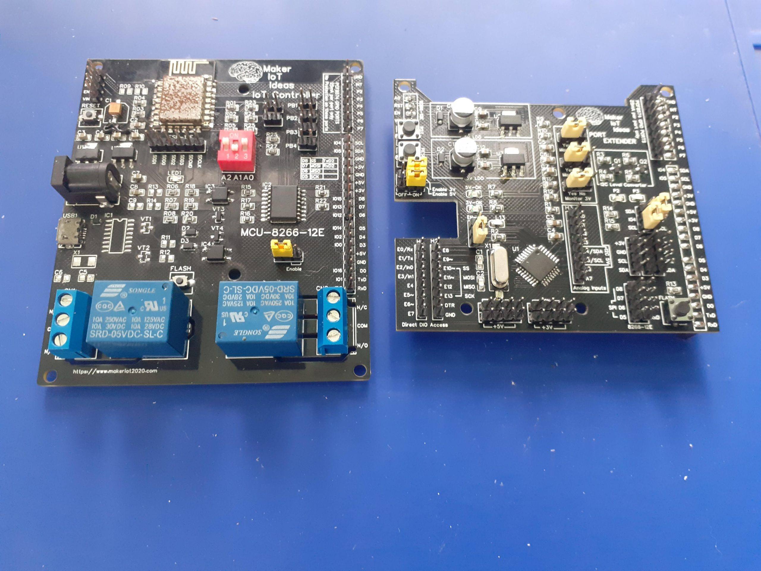
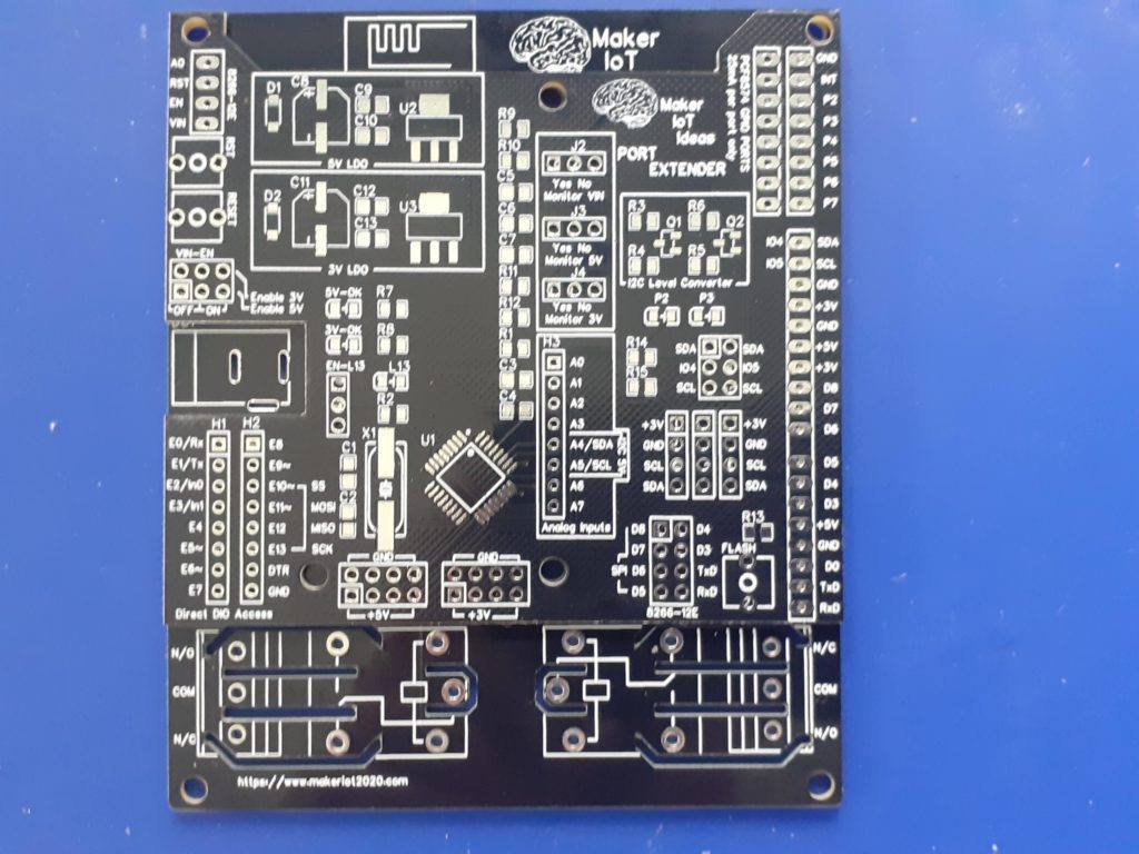
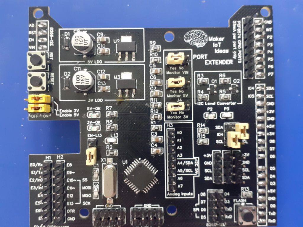
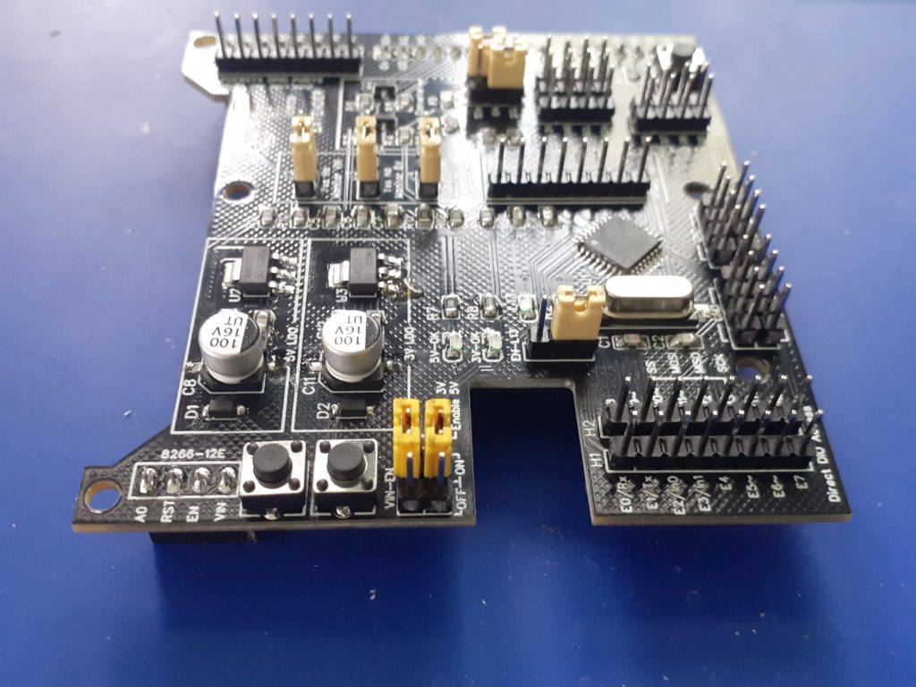
After quite a few experiments, and playing with a lot of ideas, we have finally produced and tested an almost final prototype for the MCU-8266-12E IoT Controller Port Extender Card. While the baseboard already has quite a lot of free GPIO pins for additional sensors and devices, It did however have quite a few issues, namely a lack of sufficient Power outputs, difficulty access to the I2C bus, as well as only 2 relay outputs. Granted that you do have access to unused pins on the PCF8574 Port Extender, We nonetheless decided that an add-on card would definitely make sense to allow this device to really be more useable.
While looking at various ideas for this card, the most flexible seemed to be the APE Protocol device as documented in ESPHome. They used a standard Arduino board for that, but we decided that, after testing it with an Arduino Nano, since it seems to work well, let us just design a dedicated PCB. It also looks much better as well 🙂
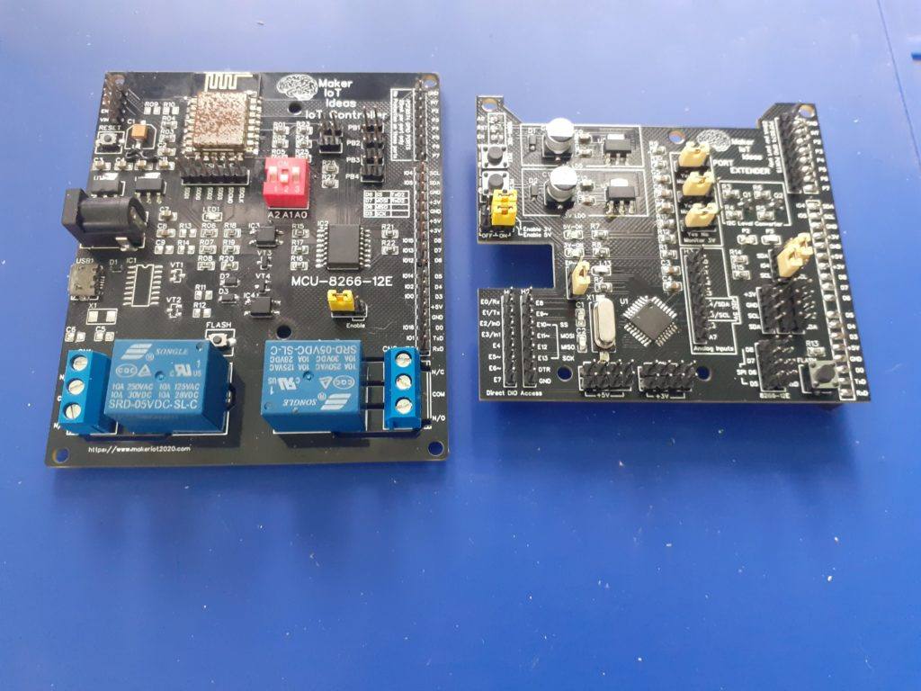
The beginning of the APE (Arduino Port Extender) Device. MCU-8266-12E with Arduino Nano (left) and MCU-8266-12E with the newly designed APE Card (right)
Some Features (Aside from being a fully functional Arduino clone as well)
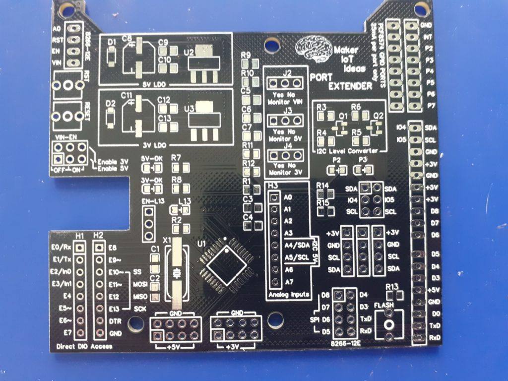
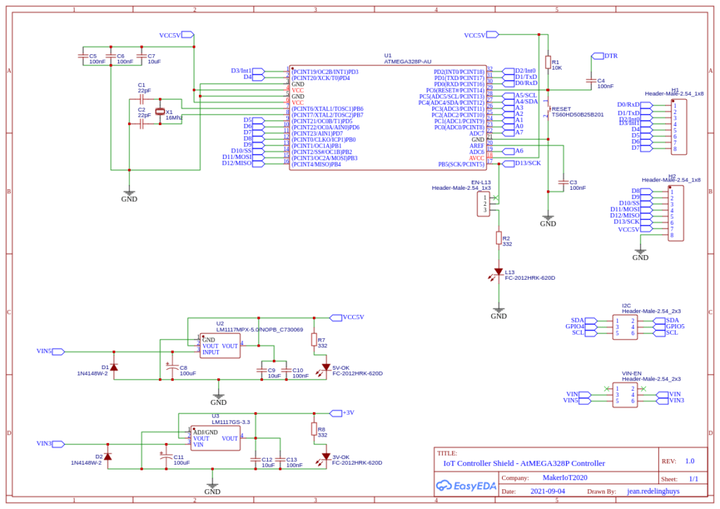
1). Dedicated LDO Regulators for 5v and 3.3v (800mA each), with jumpers to switch them on or off (receive power only from the IoT Motherboard). 2.) Dedicated Logic Level Converter on the I2C Bus ( This is sort of very much needed 🙂 The Atmega 328P-AU is running at 5v on this device, to enable it to run at 16Mhz.. and the ESP8266 on the Motherboard is a 3.3v device..
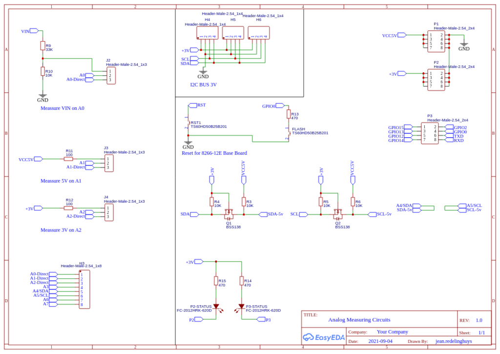
There are also 3x 3.3V I2C Headers, complete with 3.3v and Ground, as well as a single 5v I2C header 3). 8 Analog Inputs ( While practically you can only use 6 of these if you use I2C ) 4). Voltage Divider provided on A0 to measure VIN ( to be safe, we calculated the resistors for 22v) 5). 100R current limiting resistor on A1 and A2, to measure 5v and 3.3v as well… Analog inputs A0, A1 and A2 can be switched back to normal operation by changing the jumper at J2,J3 or J4 from On to Off. 6). 12 Digital Inputs/Outputs (14 if you use D0 and D1 as well), as well as a Jumper to remove the LED on D13. 7). Full access to the PCF8574 and ESP8266 Pins from the motherboard below.
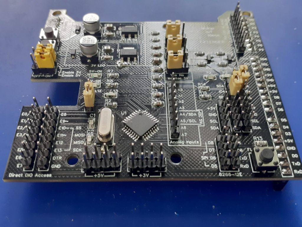
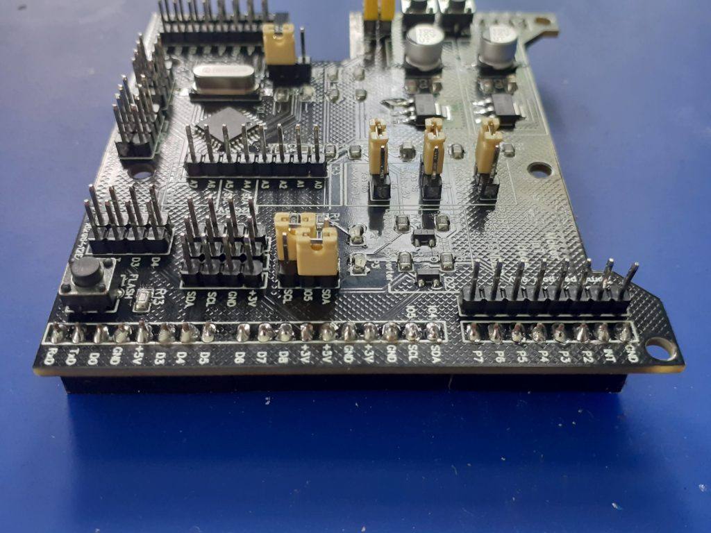
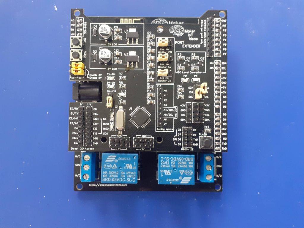
Pictures of the PCB
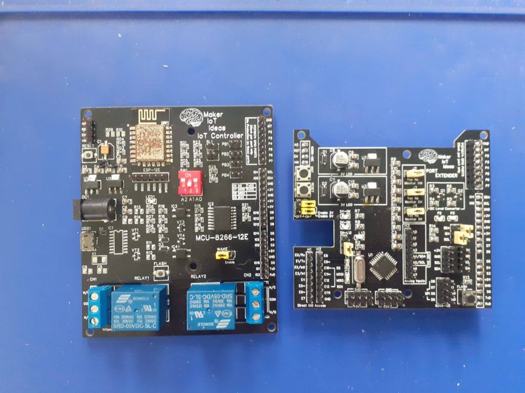
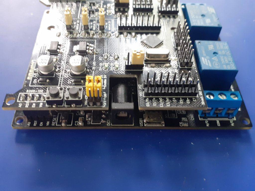
Side by side MCU-8266-12E (left) 8266-12E-Port Extender (right)
Side by side MCU-8266-12E (left) 8266-12E-Port Extender (right)
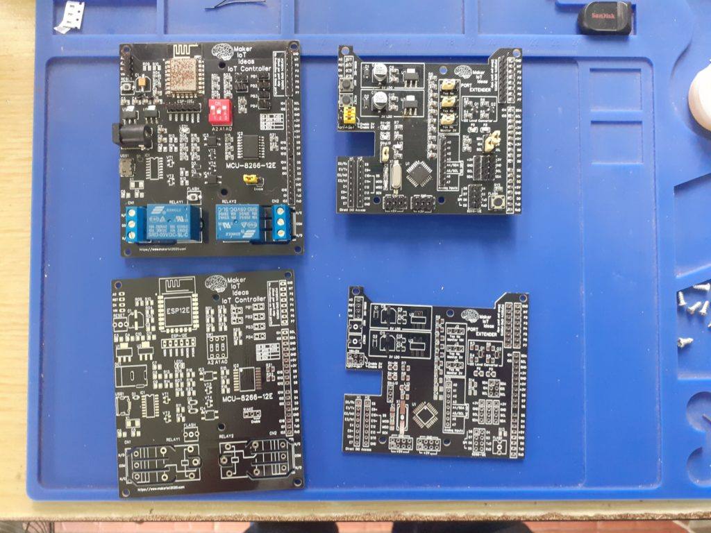
Side by side MCU-8266-12E (left) 8266-12E-Port Extender (right) [ with unpopulated PCB at bottom]
Blank PCB 8266-12E-Port Extender
Blank PCB MCU-8266-12E IoT Controller
Top view 8266-12E PE
8266-12E-PE side view { from bottom)
Right side view – 8266-12E-PE
Left side view – 8266-12E-PE
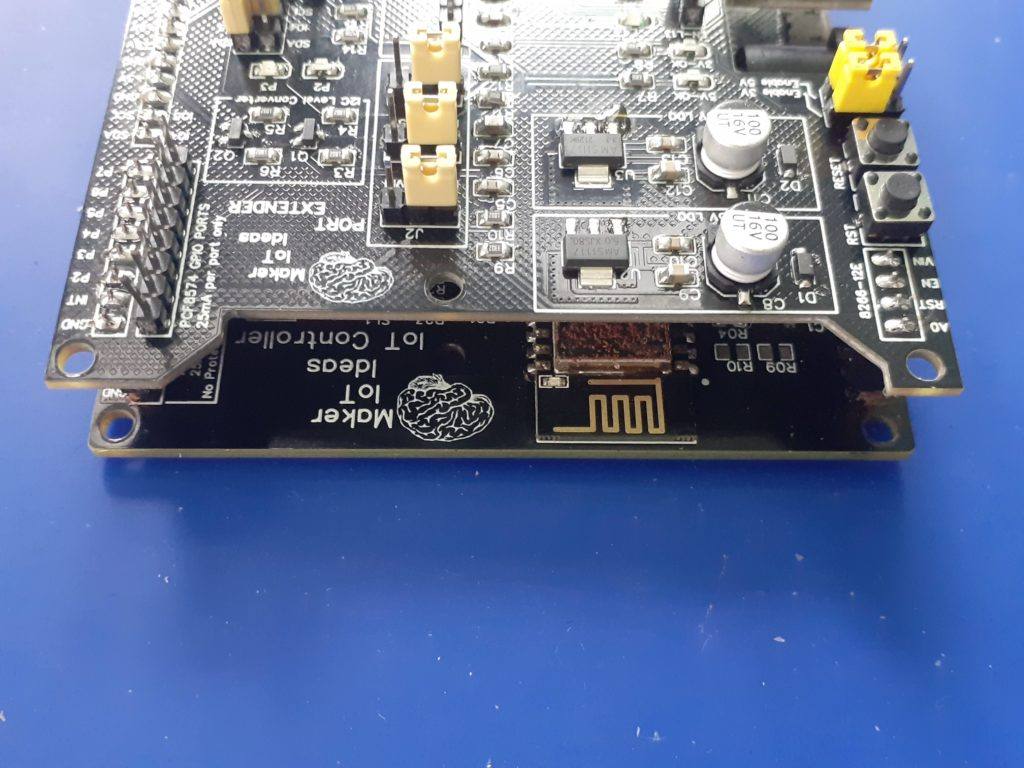
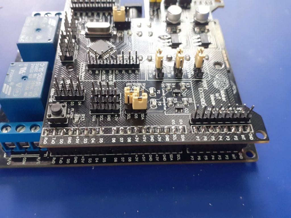
Stacked on-top-of MCU-8266-12E
Stacked – Top Side view
Stacked – Right side view
Stacked – Left side view
Pictures of the PCB, alone and with the MCU-8266-12E IoT controller
Circuit Diagram
ATMega328P-AU Circuit diagram with LDO Regulators, headers and supporting circuitry.Analog measuring circuitry, level converters and supporting circuitry and headers
Uploading Code to the ATMega328P
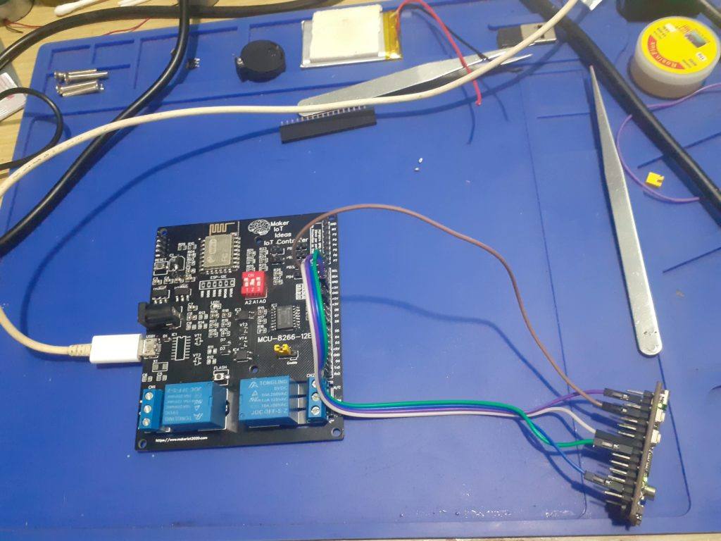
Uploading code to the device requires the use of either an ISCP programmer ( Arduino as ISP works well ) or in the case of a pre-boot loaded chip, a USB-to-Serial converter. We did not find it necessary to add a dedicated USB-to-Serial converter onto the PCB. It is quite easy enough to do any flashing with the tools mentioned above.
Make sure that the PCB is not stacked when doing this. ( This will prevent excessive current use of other components when you supply 5v to the PE card.
Procedure to upload using ICSP
During assembly, you are required to solder a single 90-degree bend pin header on the bottom side of the PCB, in the same hole as the board side edge of the RESET push-button. This will serve as the RESET Pin for the ISCP. Other connections are as follows:
H2 Header <- > ICSP Programmer MOSI (E11~) – MOSI ( or Pin 11 on Arduino as ISP ) MISO (E12 ) – MISO ( or Pin 12 on Arduino as ISP ) SCK (E13) – D13 (or Pin 13 on Arduino as ISP ) RESET – D10 (or Pin 10 on Arduino as ISP )
5v and Ground from Arduino as ISP or ISCP Programmer to any 5v and ground pin on the PE Card
Please note the description above for assembly of the RESET pin header
Procedure to upload using USB-to-Serial converter
H1 Header
E0/Rx <- to Tx of USB-to-Serial converter E1/Tx -> to Rx of USB-to-Serial converter
H2 Header
DTR <-> to DTR of USB-to-Serial converter [ This connection is needed for successful uploading. Don’t leave it out ]
5v and Ground from the USB-to-Serial converter to any 5v and ground pin on the PE Card
Testing with ESPHome APE protocol and the MCU-8266-12E IoT controller
The following Arduino Sketch needs to be uploaded to the device. It will allow the device to function as a custom I2C device. Feel free to change the I2C address in the sketch as you choose, but remember to use the same address in your ESPHome YAML configuration file
The following C header file needs to be uploaded to your Home Assistant ESPHome folder.
// Must disable logging if using logging in main.cpp or in other custom components for the
//  __c causes a section type conflict with __c thingy
// you can enable logging and use it if you enable this in logger:
/*
logger:
  level: DEBUG
  esp8266_store_log_strings_in_flash: False
  */

//#define APE_LOGGING

// take advantage of LOG_ defines to decide which code to include
#ifdef LOG_BINARY_OUTPUT
#define APE_BINARY_OUTPUT
#endif
#ifdef LOG_BINARY_SENSOR
#define APE_BINARY_SENSOR
#endif
#ifdef LOG_SENSOR
#define APE_SENSOR
#endif

static const char *TAGape = "ape";

#define APE_CMD_DIGITAL_READ 0
#define APE_CMD_WRITE_ANALOG 2
#define APE_CMD_WRITE_DIGITAL_HIGH 3
#define APE_CMD_WRITE_DIGITAL_LOW 4
#define APE_CMD_SETUP_PIN_OUTPUT 5
#define APE_CMD_SETUP_PIN_INPUT_PULLUP 6
#define APE_CMD_SETUP_PIN_INPUT 7
// 8 analog registers.. A0 to A7
// A4 and A5 not supported due to I2C
#define CMD_ANALOG_READ_A0 0b1000 // 0x8
// ....
#define CMD_ANALOG_READ_A7 0b1111 // 0xF

#define CMD_SETUP_ANALOG_INTERNAL 0x10
#define CMD_SETUP_ANALOG_DEFAULT 0x11

#define get_ape(constructor) static_cast<ArduinoPortExpander *>(constructor.get_component(0))

#define ape_binary_output(ape, pin) get_ape(ape)->get_binary_output(pin)
#define ape_binary_sensor(ape, pin) get_ape(ape)->get_binary_sensor(pin)
#define ape_analog_input(ape, pin) get_ape(ape)->get_analog_input(pin)

class ArduinoPortExpander;

using namespace esphome;

#ifdef APE_BINARY_OUTPUT
class ApeBinaryOutput : public output::BinaryOutput
{
public:
  ApeBinaryOutput(ArduinoPortExpander *parent, uint8_t pin)
  {
    this->parent_ = parent;
    this->pin_ = pin;
  }
  void write_state(bool state) override;
  uint8_t get_pin() { return this->pin_; }

protected:
  ArduinoPortExpander *parent_;
  uint8_t pin_;
  // Pins are setup as output after the state is written, Arduino has no open drain outputs, after setting an output it will either sink or source thus activating outputs writen to false during a flick.
  bool setup_{true};
  bool state_{false};

  friend class ArduinoPortExpander;
};
#endif

#ifdef APE_BINARY_SENSOR
class ApeBinarySensor : public binary_sensor::BinarySensor
{
public:
  ApeBinarySensor(ArduinoPortExpander *parent, uint8_t pin)
  {
    this->pin_ = pin;
  }
  uint8_t get_pin() { return this->pin_; }

protected:
  uint8_t pin_;
};
#endif

#ifdef APE_SENSOR
class ApeAnalogInput : public sensor::Sensor
{
public:
  ApeAnalogInput(ArduinoPortExpander *parent, uint8_t pin)
  {
    this->pin_ = pin;
  }
  uint8_t get_pin() { return this->pin_; }

protected:
  uint8_t pin_;
};
#endif

class ArduinoPortExpander : public Component, public I2CDevice
{
public:
  ArduinoPortExpander(I2CBus *bus, uint8_t address, bool vref_default = false)
  {
    set_i2c_address(address);
    set_i2c_bus(bus);
    this->vref_default_ = vref_default;
  }
  void setup() override
  {
#ifdef APE_LOGGING
    ESP_LOGCONFIG(TAGape, "Setting up ArduinoPortExpander at %#02x ...", address_);
#endif

    /* We cannot setup as usual as arduino boots later than esp8266
            Poll i2c bus for our Arduino for a n seconds instead of failing fast,
            also this is important as pin setup (INPUT_PULLUP, OUTPUT it's done once)
        */
    this->configure_timeout_ = millis() + 5000;
  }
  void loop() override
  {
    if (millis() < this->configure_timeout_)
    {
      bool try_configure = millis() % 100 > 50;
      if (try_configure == this->configure_)
        return;
      this->configure_ = try_configure;

      if (ERROR_OK == this->read_register(APE_CMD_DIGITAL_READ, const_cast<uint8_t *>(this->read_buffer_), 3))
      {
#ifdef APE_LOGGING
        ESP_LOGCONFIG(TAGape, "ArduinoPortExpander found at %#02x", address_);
#endif
        delay(10);
        if (this->vref_default_)
        {
          this->write_register(CMD_SETUP_ANALOG_DEFAULT, nullptr, 0); // 0: unused
        }

        // Config success
        this->configure_timeout_ = 0;
        this->status_clear_error();
#ifdef APE_BINARY_SENSOR
        for (ApeBinarySensor *pin : this->input_pins_)
        {
          App.feed_wdt();
          uint8_t pinNo = pin->get_pin();
#ifdef APE_LOGGING
          ESP_LOGCONFIG(TAGape, "Setup input pin %d", pinNo);
#endif
          this->write_register(APE_CMD_SETUP_PIN_INPUT_PULLUP, &pinNo, 1);
          delay(20);
        }
#endif
#ifdef APE_BINARY_OUTPUT
        for (ApeBinaryOutput *output : this->output_pins_)
        {
          if (!output->setup_)
          { // this output has a valid value already
            this->write_state(output->pin_, output->state_, true);
            App.feed_wdt();
            delay(20);
          }
        }
#endif
#ifdef APE_SENSOR
        for (ApeAnalogInput *sensor : this->analog_pins_)
        {
          App.feed_wdt();
          uint8_t pinNo = sensor->get_pin();
#ifdef APE_LOGGING
          ESP_LOGCONFIG(TAGape, "Setup analog input pin %d", pinNo);
#endif
          this->write_register(APE_CMD_SETUP_PIN_INPUT, &pinNo, 1);
          delay(20);
        }
#endif
        return;
      }
      // Still not answering
      return;
    }
    if (this->configure_timeout_ != 0 && millis() > this->configure_timeout_)
    {
#ifdef APE_LOGGING
      ESP_LOGE(TAGape, "ArduinoPortExpander NOT found at %#02x", address_);
#endif
      this->mark_failed();
      return;
    }

#ifdef APE_BINARY_SENSOR
    if (ERROR_OK != this->read_register(APE_CMD_DIGITAL_READ, const_cast<uint8_t *>(this->read_buffer_), 3))
    {
#ifdef APE_LOGGING
      ESP_LOGE(TAGape, "Error reading. Reconfiguring pending.");
#endif
      this->status_set_error();
      this->configure_timeout_ = millis() + 5000;
      return;
    }
    for (ApeBinarySensor *pin : this->input_pins_)
    {
      uint8_t pinNo = pin->get_pin();

      uint8_t bit = pinNo % 8;
      uint8_t value = pinNo < 8 ? this->read_buffer_[0] : pinNo < 16 ? this->read_buffer_[1] : this->read_buffer_[2];
      bool ret = value & (1 << bit);
      if (this->initial_state_)
        pin->publish_initial_state(ret);
      else
        pin->publish_state(ret);
    }
#endif
#ifdef APE_SENSOR
    for (ApeAnalogInput *pin : this->analog_pins_)
    {
      uint8_t pinNo = pin->get_pin();
      pin->publish_state(analogRead(pinNo));
    }
#endif
    this->initial_state_ = false;
  }

#ifdef APE_SENSOR
  uint16_t analogRead(uint8_t pin)
  {
    bool ok = (ERROR_OK == this->read_register((uint8_t)(CMD_ANALOG_READ_A0 + pin), const_cast<uint8_t *>(this->read_buffer_), 2));
#ifdef APE_LOGGING
    ESP_LOGVV(TAGape, "analog read pin: %d ok: %d byte0: %d byte1: %d", pin, ok, this->read_buffer_[0], this->read_buffer_[1]);
#endif
    uint16_t value = this->read_buffer_[0] | ((uint16_t)this->read_buffer_[1] << 8);
    return value;
  }
#endif

#ifdef APE_BINARY_OUTPUT
  output::BinaryOutput *get_binary_output(uint8_t pin)
  {
    ApeBinaryOutput *output = new ApeBinaryOutput(this, pin);
    output_pins_.push_back(output);
    return output;
  }
#endif
#ifdef APE_BINARY_SENSOR
  binary_sensor::BinarySensor *get_binary_sensor(uint8_t pin)
  {
    ApeBinarySensor *binarySensor = new ApeBinarySensor(this, pin);
    input_pins_.push_back(binarySensor);
    return binarySensor;
  }
#endif
#ifdef APE_SENSOR
  sensor::Sensor *get_analog_input(uint8_t pin)
  {
    ApeAnalogInput *input = new ApeAnalogInput(this, pin);
    analog_pins_.push_back(input);
    return input;
  }
#endif
  void write_state(uint8_t pin, bool state, bool setup = false)
  {
    if (this->configure_timeout_ != 0)
      return;
#ifdef APE_LOGGING
    ESP_LOGD(TAGape, "Writing %d to pin %d", state, pin);
#endif
    this->write_register(state ? APE_CMD_WRITE_DIGITAL_HIGH : APE_CMD_WRITE_DIGITAL_LOW, &pin, 1);
    if (setup)
    {
      App.feed_wdt();
      delay(20);
#ifdef APE_LOGGING
      ESP_LOGI(TAGape, "Setup output pin %d", pin);
#endif
      this->write_register(APE_CMD_SETUP_PIN_OUTPUT, &pin, 1);
    }
  }

protected:
  bool configure_{true};
  bool initial_state_{true};
  uint8_t read_buffer_[3]{0, 0, 0};
  unsigned long configure_timeout_{5000};
  bool vref_default_{false};

#ifdef APE_BINARY_OUTPUT
  std::vector<ApeBinaryOutput *> output_pins_;
#endif
#ifdef APE_BINARY_SENSOR
  std::vector<ApeBinarySensor *> input_pins_;
#endif
#ifdef APE_SENSOR
  std::vector<ApeAnalogInput *> analog_pins_;
#endif
};

#ifdef APE_BINARY_OUTPUT
void ApeBinaryOutput::write_state(bool state)
{
  this->state_ = state;
  this->parent_->write_state(this->pin_, state, this->setup_);
  this->setup_ = false;
}
#endif
The file should be named “arduino_port_expander.h”
Make the following changes to your ESPHome YAML configuration file for the MCU-8266-12E device
esphome:
  name: mcu-8266-12e-01
  platform: ESP8266
  board: nodemcuv2
  includes:
      - arduino_port_expander.h
# Note the include file - This loads the APE Header

# Enable logging
logger:

# Enable Home Assistant API
api:

ota:
  password: "<your password will be different - dont change it>"

wifi:
  ssid: <your ssid>
  password: <your password>

  # Enable fallback hotspot (captive portal) in case wifi connection fails
  ap:
    ssid: "MCU-8266-Hotspot"
    password: "password"

captive_portal:

i2c:
# PCB Prototype
  sda: GPIO5
  scl: GPIO4
# PCB Rev 1.5 or higher, comment the above 2 lines
# and uncomment
#sda: GPIO4
#scl: GPIO5
#################### - IMPORTANT ###########
  scan: true
  id: i2c_bus_a

pcf8574:
  - id: 'pcf8574_hub'
    address: 0x22 # Set at 0x22, feel free to change to your liking, Remember to set the chip to the address you choose as well
    pcf8575: false

time:
  - platform: sntp
    id: ha_time
    timezone: "Etc/GMT+7"

status_led:
  pin:
    number: GPIO16
    inverted: true

#Define the APE as a custom component, taking care to ensure that:
#1). The I2C Bust ID is the same as the one you have defined in the I2C: Section
#2). The address of the APE is the same as the one you set in the sketch

custom_component:
  - id: ape
    lambda: |-
      auto ape_component = new ArduinoPortExpander(i2c_bus_a, 0x08,true);
      return {ape_component};


sensor:

  - platform: custom
    lambda: |-
      return {ape_analog_input(ape, 0),  // 1 = A1
             ape_analog_input(ape, 1),
             ape_analog_input(ape, 2)};

#We define 3 analog inputs (A0,A1,A2) to monitor voltages on the card
#Note that you MUST define them in the sensors section below as well AND
#THAT THEY MUST BE IN THE SAME SEQUENCE THAT YOU DEFINED THEM IN ABOVE HERE
#
#ALSO NOTE THAT YOU CAN "NOT" use A4 and A5, as they are used for I2C !
#
# As an example, of adding another 3 analog inputs, your definition above will change to:
#
#    return {ape_analog_input(ape, 0),
#           ape_analog_input(ape, 1),
#           ape_analog_input(ape, 2),
#           ape_analog_input(ape, 3),
#           ape_analog_input(ape, 6),
#           ape_analog_input(ape, 7)};
#
#
# Now define the sensors connected to these analogs below:


    sensors:
      - name: "PE Card VIN"
        id: analog_a0
        device_class: "voltage"
        unit_of_measurement: "v"
        accuracy_decimals: 2
        filters:
          - lambda: return x * (22.00/1023.0);
          - throttle: 60s

# We use a lambda to scale the value of VIN - Our Voltage divider was designed around 22 volt
# thus we need 22 volt here in the calculation as well to make it accurate
#
      - name: "PE Card 5v"
        id: analog_a1
        device_class: "voltage"
        unit_of_measurement: "v"
        accuracy_decimals: 2
        filters:
          - lambda: return x * (5.02/1023.0);
          - throttle: 60s
      - name: "PE Card 3v"
        id: analog_a2
        device_class: "voltage"
        unit_of_measurement: "v"
        accuracy_decimals: 2
        filters:
          - lambda: return x * (5.02/1023.0);
          - throttle: 60s

# The ATMega328P 's Analog Reference is set to 5v internally, thus we need to also scale the
# 3v input with a maximum of 5v ...

# In case you enabled the other 3 Analog Inputs above, you need to add the following
#
#    - name: "Analog 3"
#      id: analog_a3
#      filters:
#        - throttle: 60s
#    - name: "Analog 6"
#      id: analog_a6
#      filters:
#        - throttle: 60s
#    - name: "Analog 7"
#      id: analog_a7
#      filters:
#        - throttle: 60s
#
#


  - platform: adc
    pin: VCC
    name: "ESP8266 Chip Voltage"
    id: mcu_voltage
    unit_of_measurement: "V"
    device_class: "voltage"
    accuracy_decimals: 2
    update_interval: 60s

  - platform: wifi_signal
    name: "WiFi Signal Sensor"
    id: wifi_strength
    device_class: "signal_strength"
    unit_of_measurement: "dBm"
    update_interval: 240s


#Digital outputs function the same

output:
- platform: custom
  type: binary
  lambda: |-
    return {ape_binary_output(ape, 2),
            ape_binary_output(ape, 3),
            ape_binary_output(ape, 4),
            ape_binary_output(ape, 5),
            ape_binary_output(ape, 6),
            ape_binary_output(ape, 7)};
  outputs:
    - id: ape_output_p2
      inverted: false
    - id: ape_output_p3
      inverted: false
    - id: ape_output_p4
      inverted: false
    - id: ape_output_p5
      inverted: false
    - id: ape_output_p6
      inverted: false
    - id: ape_output_p7
      inverted: false

- platform: gpio
  id: relay_1
  pin:
    pcf8574: pcf8574_hub
    number: 0
    mode: OUTPUT
    inverted: true
- platform: gpio
  id: relay_2
  pin:
    pcf8574: pcf8574_hub
    number: 1
    mode: OUTPUT
    inverted: true
- platform: gpio
  id: led_status_1
  pin:
    pcf8574: pcf8574_hub
    number: 2
    mode: OUTPUT
    inverted: true
- platform: gpio
  id: led_status_2
  pin:
    pcf8574: pcf8574_hub
    number: 3
    mode: OUTPUT
    inverted: true

binary_sensor:
  - platform: gpio
    id: push_button_1
    name: 'Relay1 Pushbutton'
    device_class: ''
    pin:
      pcf8574: pcf8574_hub
      number: 4
      mode: INPUT
      inverted: true
    on_press:
      then:
        - switch.toggle: switch_relay1

  - platform: gpio
    id: push_button_2
    name: 'Relay2 Pushbutton'
    device_class: ''
    pin:
      pcf8574: pcf8574_hub
      number: 5
      mode: INPUT
      inverted: true
    on_press:
      #min_length: 50ms
      #max_length: 500ms
      then:
        - switch.toggle: switch_relay2
    filters:
        - delayed_on_off: 50ms


switch:
  - platform: output
    id: switch_relay1
    name: "Relay No. 1 (#0)"
    output: relay_1
    on_turn_on:
      - output.turn_on: led_status_1
    on_turn_off:
      - output.turn_off: led_status_1

  - platform: output
    id: switch_relay2
    name: "Relay No. 2 (#1)"
    output: relay_2
    on_turn_on:
      - output.turn_on: led_status_2
    on_turn_off:
      - output.turn_off: led_status_2
  - platform: restart
    id: reboot_switch
    name: "Reboot Me"
This PCB was manufactured at PCBWAY. The Gerber files and BOM, as well as all the schematics, will soon be available as a shared project on their website. If you would like to have PCBWAY manufacture one of your own, designs, or even this particular PCB, you need to do the following… 1) Click on this link 2) Create an account if you have not already got one of your own. If you use the link above, you will also instantly receive a $5USD coupon, which you can use on your first or any other order later. (Disclaimer: I will earn a small referral fee from PCBWay. This referral fee will not affect the cost of your order, nor will you pay any part thereof.) 3) Once you have gone to their website, and created an account, or login with your existing account,
4) Click on PCB Instant Quote
5) If you do not have any very special requirements for your PCB, click on Quick-order PCB
6) Click on Add Gerber File, and select your Gerber file(s) from your computer. Most of your PCB details will now be automatically selected, leaving you to only select the solder mask and silk-screen colour, as well as to remove the order number or not. You can of course fine-tune everything exactly as you want as well.
7) You can also select whether you want an SMD stencil, or have the board assembled after manufacturing. Please note that the assembly service, as well as the cost of your components, ARE NOT included in the initial quoted price. ( The quote will update depending on what options you select ).
8) When you are happy with the options that you have selected, you can click on the Save to Cart Button. From here on, you can go to the top of the screen, click on Cart, make any payment(s) or use any coupons that you have in your account.
Then just sit back and wait for your new PCB to be delivered to your door via the shipping company that you have selected during checkout.