
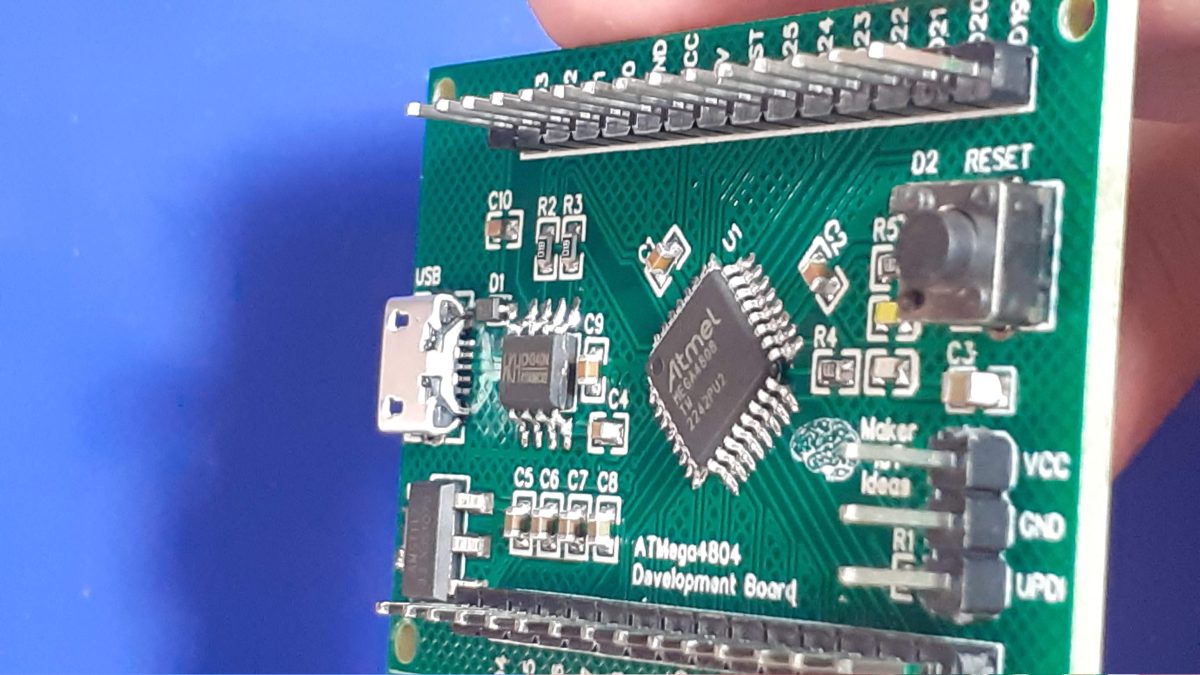
The ATMEGA4808 provides a very attractive solution to replace the trusted ATMEGA328 or standard Arduino UNO /NANO.
These chips are slightly more difficult to get hold of than the ATTiny chips, and cost a little bit more ( about the same as what the ATMEGA328 used to cost before the mess with COVID-19 and resulting supply chain shortages + inflated costs), but they offer all of the functions of the ATMEGA328, with a few other enhancements that will definitely be very useful.

The extras include:
– Hardware interrupts on ALL GPIO pins; This is way more than the standard 2 interrupts on the ATMEGA328 ( We are not talking about the Pin Change interrupts, but real hardware interrupts, that can be triggered on RISING, FALLING, CHANGE, HIGH and LOW state of each pin
– Up to eight (8) PWM pins as opposed to the 6 on the Arduino UNO
– Up to eleven Analog inputs
– An Analog Comparator module
– Configurable Custom Logic (CCL)
– EVENT System (EVSYS)
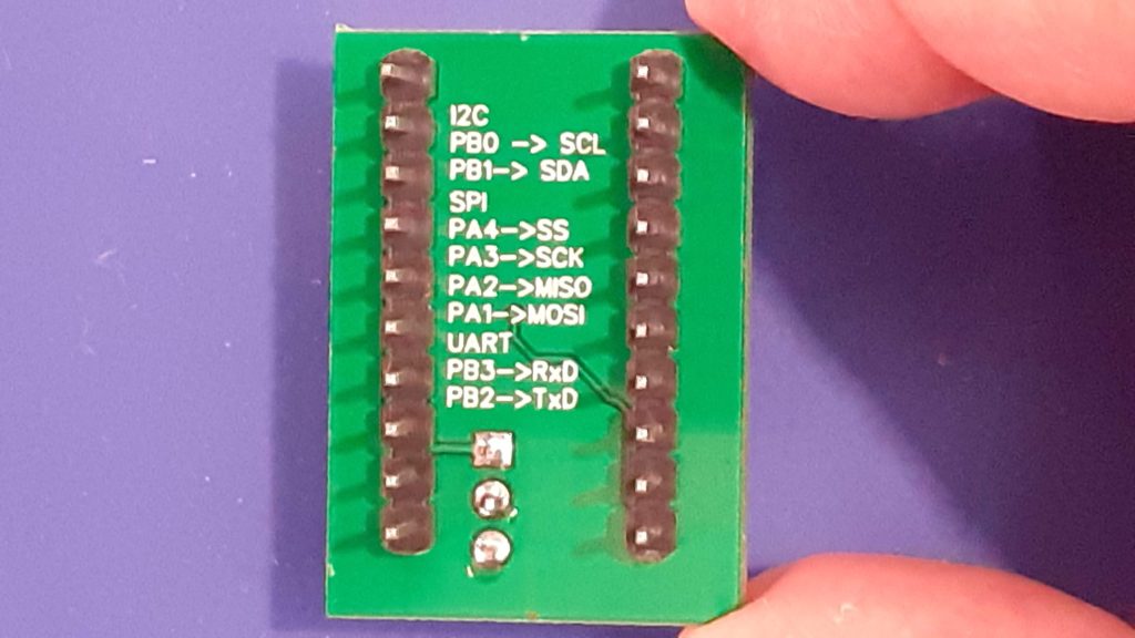
– Peripheral pin swapping
It is also worth mentioning that these chips have accurate internal oscillators, capable of clocking the chip at up to 20MHz, further reducing the number of external components required to get a minimal configuration running…
Order your own version of this development board
The Prototype PCB
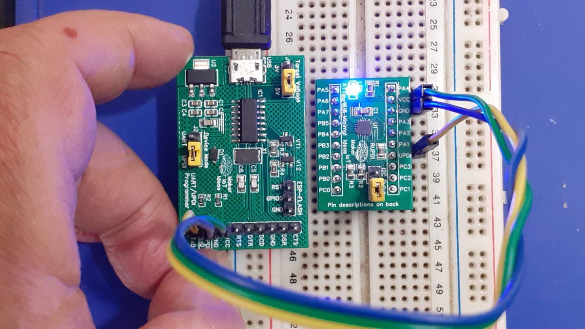
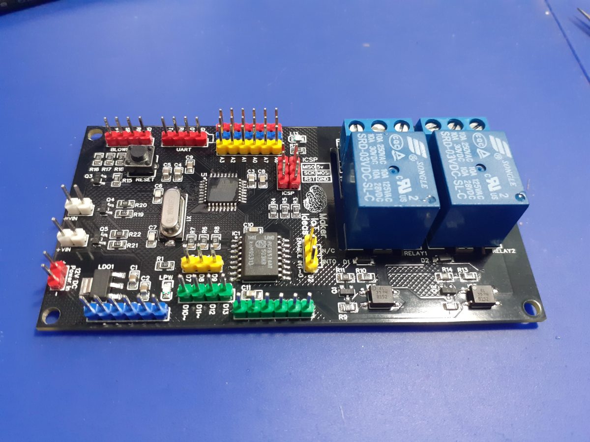
While I have had a Nano Every “Clone” lying in a drawer for quite a while now, I did not really pay a lot of attention to it. That was, until I needed an ATMEGA328 for a project, and could not find any for sale, or at least at a price that I was willing to pay for it… That incident was the spark that ignited this entire exercise, to find a suitable replacement…
The Nano Every “Clone” in my possession, used the ATMEGA 4808 chip and turned out to be the Thinary Nano 4808. I had quite a lot of problems with the provided core, as well as getting peripherals like I2c and SPI to work. This led to further investigations, and finally, I decided on building my own and to use the MCUdude/MegaCoreX Arduino Core to program it.
This led to the following prototype:

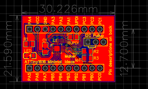
I did not bother with too much detail on the silk screen here, as the goal was to get a working board, test it, and then later, design a refined PCB.
What is important to note is that the board runs at 5v, but provides a single 3.3v output as well. Logic levels on the GPIO is also 5v. Use level converters for 3.3v only addons…
The MEGA4808 is programmed via UPDI, so we have a UPDI Header on the right-hand side of the PCB. It is also possible to use the Optiboot Bootloader, to flash the board in true Arduino style through a USB connection to a computer.
A CH340N USB-to-Serial converter chip is used instead of the CH340G that is common on the UNO clones. The CH340N provides only the USB D+ D- signals, as well as Rx, TX and RTS. RTS is being used to auto-reset the chip after flashing…
In comparison to the CH340G, which also required a crystal oscillator, but provides all the modem control signals, which, are usually not even broken out, the CH340N made much more sense.

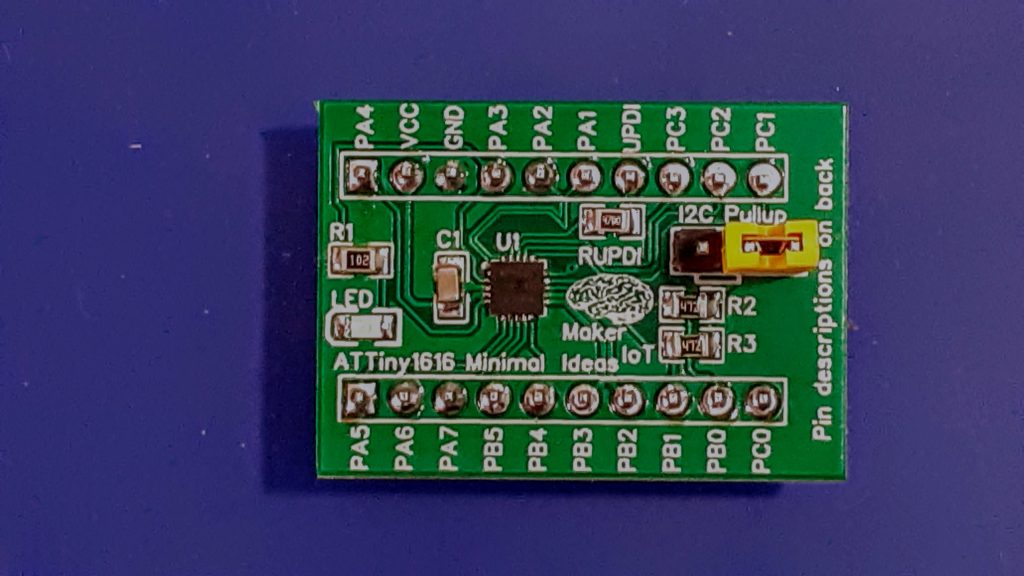
A power LED, as well as an indicator LED on pin 7 was also included.

Assembly and Soldering
I normally assemble all my projects by hand and reflow-solder them with a hot plate. for this project, I decided to do things a bit differently, which ended up being a bit awkward, but still resulted in a perfectly useable PBC.
As you will know by now, I only do written articles, as I don’t consider myself ready for the Youtube and video thing, as well as because I believe a well-written article, with detailed pictures, is easier to understand than a video…
Well, today, we will have both… This article, with its writeups and pictures, as well as a short assembly and soldering video, with no sound, sped up 5x, as I did not want to bore anyone with a 25-minute silent video…
Let us begin then…

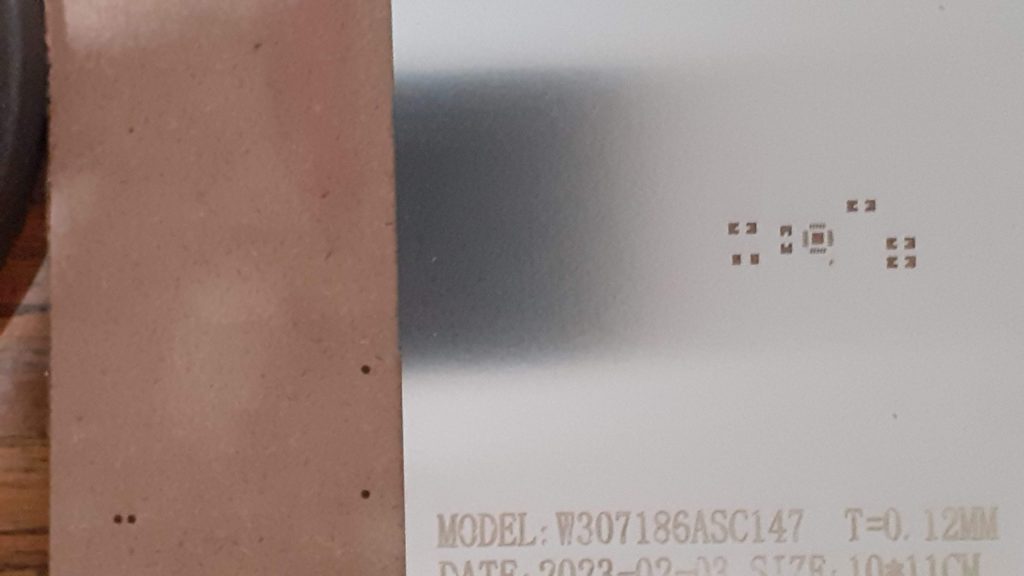
We start with a blank PCB and the laser-cut stainless steel stencil that I got from PCBWay.

Solder paste is then applied with the stencil and a scraper, and afterwards, the stencil is removed… The PCB is now ready for component placement…
From here on, we will go to the video footage… showing component placement, with some awkwardness due to the camera being in the way, as well as hot-air soldering, with the same awkwardness, as I was forced to use my right hand ( I am left-handed), not to block the camera view…
Begin quite new to the video thing, I have also not quite figured out the editing software, so the video is in native resolution… not zoomed…

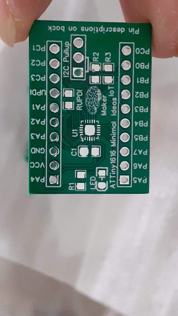
After assembly, I checked for solder bridges and was quite happy that there were none. This also meant that the board worked perfectly the first time around… as it should…
Order your own version of this development board
Manufacturing
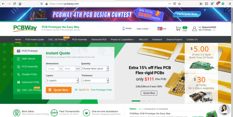
I choose PCBWay for my PCB manufacturing. Why? What makes them different from the rest?
PCBWay‘s business goal is to be the most professional PCB manufacturer for prototyping and low-volume production work in the world. With more than a decade in the business, they are committed to meeting the needs of their customers from different industries in terms of quality, delivery, cost-effectiveness and any other demanding requests. As one of the most experienced PCB manufacturers and SMT Assemblers in China, they pride themselves to be our (the Makers) best business partners, as well as good friends in every aspect of our PCB manufacturing needs. They strive to make our R&D work easy and hassle-free.
How do they do that?
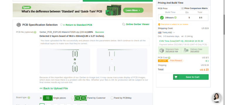
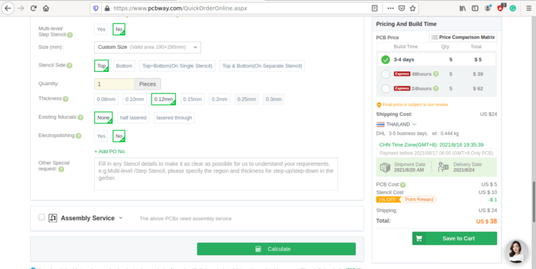
PCBWay is NOT a broker. That means that they do all manufacturing and assembly themselves, cutting out all the middlemen, and saving us money.
PCBWay’s online quoting system gives a very detailed and accurate picture of all costs upfront, including components and assembly costs. This saves a lot of time and hassle.
PCBWay gives you one-on-one customer support, that answers you in 5 minutes ( from the Website chat ) , or by email within a few hours ( from your personal account manager). Issues are really resolved very quickly, not that there are many anyway, but, as we are all human, it is nice to know that when a gremlin rears its head, you have someone to talk to that will do his/her best to resolve your issue as soon as possible.
Find out more here

Picture Gallery


