A few months ago, I started working on an MCU Card design, which borrows from the idea of a standard desktop PC, in which there are a main-board, MCU and expansion slots, to add and remove peripherals as needed quickly.
The ESP-12E Card is a continuation of that project, with the ultimate goal to have a universal “main-board” that can accept various MCUs and standardised “expansion modules” that perform a specific task.
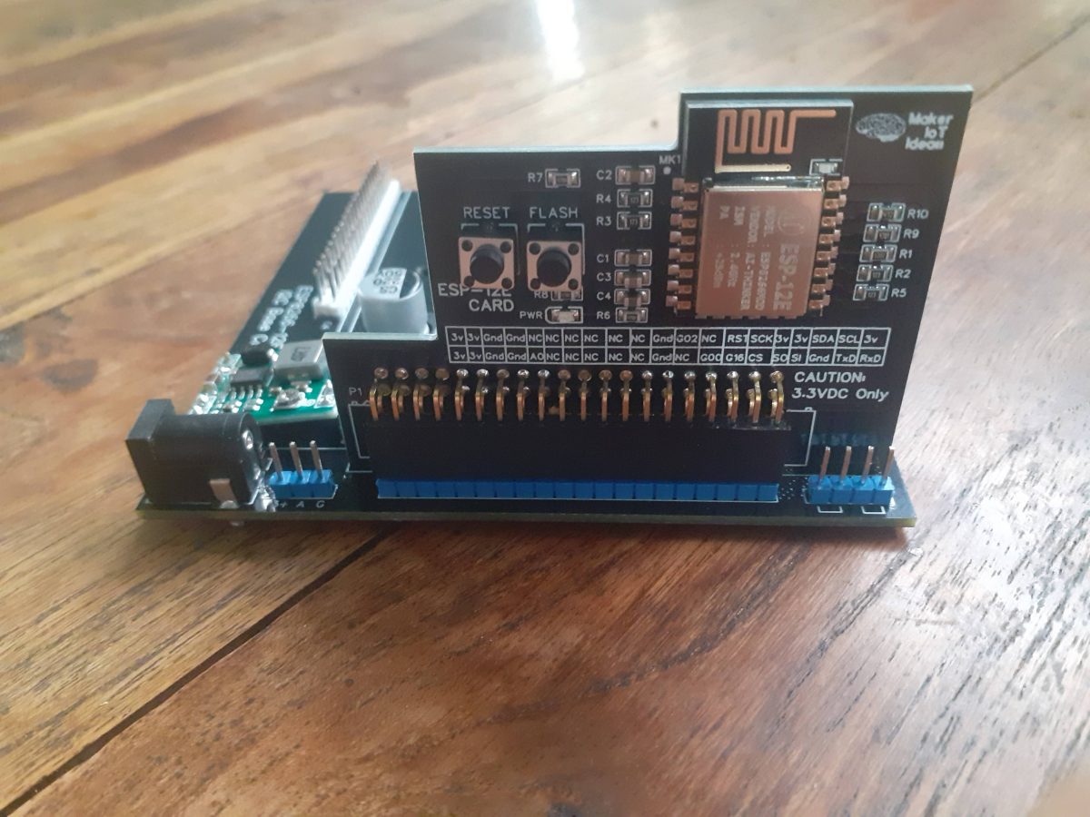
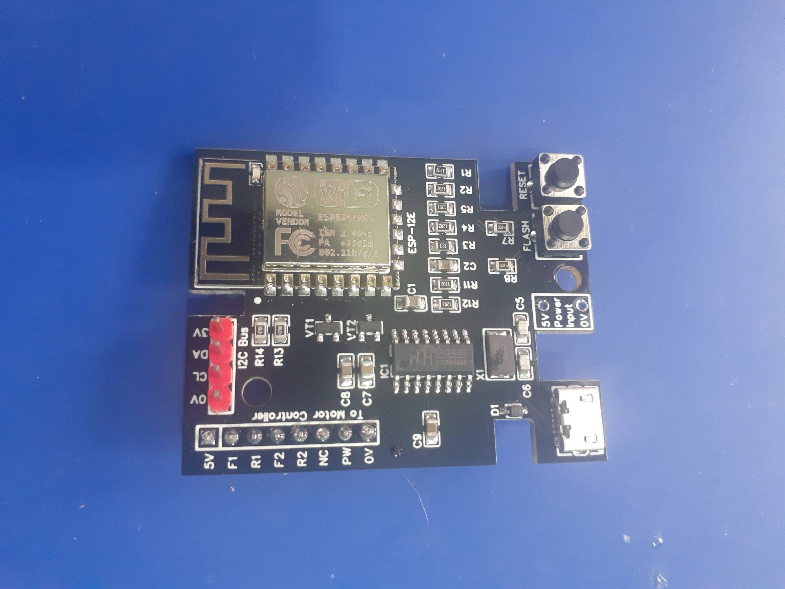
ESP-12E Card
The PCB
The ESP-12E Card contains the bare minimum components to allow the chip to function. There are no power regulators or USB-to-TTL converters onboard. Code is flashed via an external USB-to-TTL converter, with Flash and Reset buttons on the actual PCB, or available in the 2×20 Pin female header at the bottom of the card.
Most of the GPIO is also broken out to the 2×20 pin header, with the exception of the 6 GPIO that is usually connected to the internal Flash on the ESP-12E module.
I have made provision for enough power and ground pins on the header as well.
As far as GPIO is concerned, They have been grouped together by function, as much as possible at least, to make interfacing with the base-board as easy as possible.
The Schematic
ESP-12E Card Schematic
The schematic is not complicated. It is a standard ESP-8266 configuration, with all non-essential components removed.
The “base-board” ( a sneak preview )
Sneak preview of the Base Card
In a future article, I will tell you more about this ( for the time being limited to I2C ) base card. [ a quick explanation: When I mean limited to I2C, it relates to the fact that at the moment, the base card, ( a prototype ) can only communicate back to the MCU via I2C protocol from each of the expansion slots, as well as via two dedicated IRQ lines from each slot ]Power is supplied via a small SMPS module.
Manufacturing the PCB
Over the past eight years, PCBWay has continuously upgraded their MANUFACTURING plants and equipment to meet higher quality requirements, and now THEY also provide OEM services to build your products from ideas to mass production and access to the market.
The PCB for this project has been manufactured at PCBWay. Please consider supporting them if you would like your own copy of this PCB, or if you have any PCB of your own that you need to have manufactured.
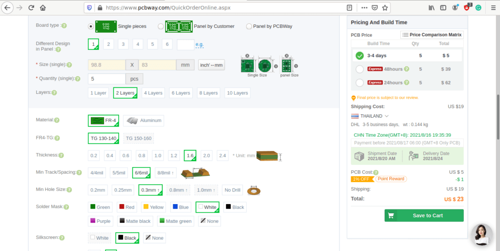
If you would like to have PCBWAY manufacture one of your own, designs, or even this particular PCB, you need to do the following… 1) Click on this link 2) Create an account if you have not already got one of your own. If you use the link above, you will also instantly receive a $5 USD coupon, which you can use on your first or any other order later. (Disclaimer: I will earn a small referral fee from PCBWay. This referral fee will not affect the cost of your order, nor will you pay any part thereof.) 3) Once you have gone to their website, and created an account, or login with your existing account,
4) Click on PCB Instant Quote
5) If you do not have any very special requirements for your PCB, click on Quick-order PCB
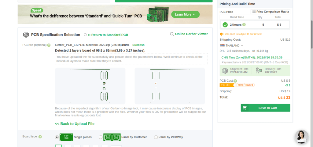
6) Click on Add Gerber File, and select your Gerber file(s) from your computer. Most of your PCB details will now be automatically selected, leaving you to only select the solder mask and silk-screen colour, as well as to remove the order number or not. You can of course fine-tune everything exactly as you want as well.
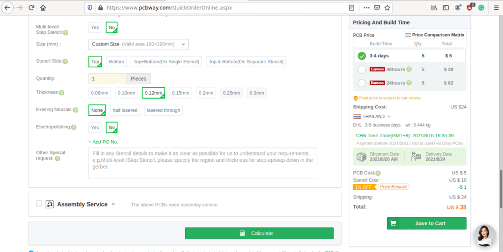
7) You can also select whether you want an SMD stencil, or have the board assembled after manufacturing. Please note that the assembly service, as well as the cost of your components, ARE NOT included in the initial quoted price. ( The quote will update depending on what options you select ).
8) When you are happy with the options that you have selected, you can click on the Save to Cart Button. From here on, you can go to the top of the screen, click on Cart, make any payment(s) or use any coupons that you have in your account.
Then just sit back and wait for your new PCB to be delivered to your door via the shipping company that you have selected during checkout.
(Design for Manufacturability) Gerber Software Analyser
Free to Use for all PCBpartner.com Users
PCBPartner.com recently decided to release their own DFM software, which I believe they developed in-house and use themselves every day, to their customers, in order to enable their customers to design better PCBs and increase the overall quality and service satisfaction.
In this article, I will give the software a quick look and feel, and show you some of its features, while at the same time admitting upfront, that it is quite complex, and that I am also not quite well acquainted with it myself, having only a few days to play with it up to now.
What is DFM?
DFM (Design for manufacturability) analysis of incoming Gerber files is a standard and important process in any PCB factory. iPCB-DFM’s purpose is to perform this process automatically to find potential production issues with your PCB design, saving time and effort for you the PCB designer, and the PCB manufacturing engineers who are going to produce your PCB. Based on 25 years of PCB manufacturing experience, we have a massive collection of PCB DFM rules built into this software, allowing it to analyze up to 24 kinds of specifications.
It also has powerful features such as quick panalization, PCB simulation and direct Gerber editing, and can even help you count how many SMD pads are in your design!
Why do you need iPCB-DFM?
If you’re an electronic engineer, you don’t want to send your PCB Gerber files for manufacturing without checking that your design and file formats match your factory’s production capability; If you are a purchasing manager without much knowledge of PCB manufacturing processes, this tool can help you better understand the specifics of the PCBs you are ordering, making it much easier to communicate with your PCB suppliers.
-PCB simulation: generate a simulated preview of your PCB, updated in real-time by different colour settings and surface finishes, and supporting high-resolution PNG output format.
DFM Functions
1 Layer 2 Dimension 3 Minimum trace space 4 Minimum trace width 5 Hole diameter 6 Drill slot 7 Through-hole annular ring 8 Hole distance 9 Hole to trace 10 Copper to edge 11 Special holes 12 SMD size 13 Via in pads 14 Test Point 15 Component solder pads number 16 Via density 17 Surface finish area (%) 18 Routing length of travel 19 Grid wiring 20 Solder mask 21 Fiducial Point 22 SMD pad size 23 SMD pad space 24 BGAs
Gerber Edit
1 Add elements 2 Delete elements 3 Move elements 4 Copy elements 5 Adjust circuit angle 6 Rotate elements 7 Edit trace 8 Mirror 9 Positive and negative switch 10 Break trace 11 Shape edit 12 Single, rectangular marquee, polygon selection
Panelization Quick panelization – set a panelization style, tooling bar width and board space, one click to generate a panalized board in seconds in Gerber format. Advanced panelization – allows you to adjust tooling hole, v-cut, fiducial mark, solder mask for fiducial mark, drill holes on tooling bar, etc.
What does it need to run?
For the foreseeable time forward, the software only runs on Microsoft Windows. It apparently supports from Windows XP right up to Windows 11, but I only had success on Windows 10, ( I don’t have Win 11).
This was also done in a VM running in Oracle Virtualbox on an Ubuntu 22.04 LTS host. (My main operating system) Specifications for the VM were 4Gb RAM and a 50Gb Hard Disk. I have also tested it with 8Gb, but it did not make any real difference to the performance. (This is most definitely NOT related to the DFM software, but more likely to be attributed to a certain heavy resource-consuming operating system (Win 10 – which as most of us know by now, is super slow whatever you give it to run on)
Installation
Installation is straightforward and quite easy, as we can expect from any Windows software these days
Getting Started
The software starts up pretty quickly, but the gets a bit of a slowdown with a login prompt tying back to PCBPartner, where you have to enter your login credentials. This can take a bit of time to actually appear.
I am hopeful that this process will in time be streamlined as I believe that the number of users on the system will grow quite fast…
Let us look at some pictures of the UI and Menu Systems
The software also comes with a very detailed Helpfile in .pdf format
This is an extremely complex piece of software. It is also extremely powerful, and can thus be very very useful to all of us. The learning curve is extremely steep, but I do believe that it will be possible to learn and use it effectively.
As a Linux user, I would also like to see a Linux version, or at least an in-browser version, similar to a well-known EDA software package. The days that software should be confined to one operating system should be behind us ( at least in my personal view, I find it very frustrating that most other commercial CAD, CAM and EDA packages are actively forcing us to stay with one of the slowest operating systems available )
I also want to thank PCBPartner for giving me the opportunity to review and take this for a test drive. I would only have wanted to be more adept at actually getting value out of a great piece of software, but I believe that I will definitely get better at it over time.
Today we will look at the remote control unit for the Robotic Toy Car – Part 6. The project is close to being completed, and as such, there are quite a lot of final things that need to be taken care of.
One of these will definitely be the final coding, which I will release in the final part of the project, so with that in mind, let us take a look at the remote control unit.
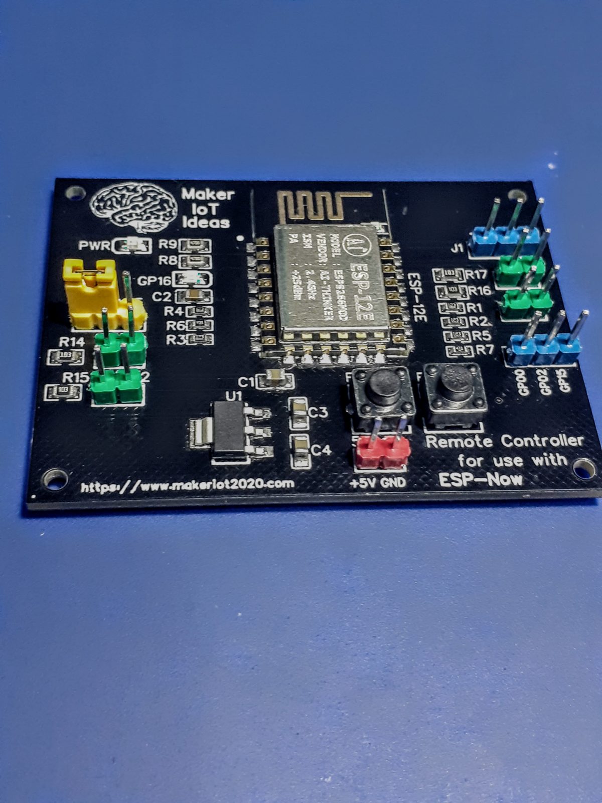
Remote Control Unit, designed to be used with ESP-Now
I have decided to do something completely different from standard remote control units, being that I will use ESP-Now, a protocol developed by Espressif. ESP-Now runs on the Wifi hardware of the ESP8266 or ESP32 and is basically a peer-to-peer protocol, that does not require Wifi but can co-exist with it on the same device. Outdoors, ESP-Now has a range of about 100m, which should work very well for my intended use.
The Remote control, as designed, will have 4 dedicated buttons: forward, reverse, left and right, divided into two groups to make two-handed control easier, similar to a standard game controller. No input on either of the two groups will result in stopping the vehicle, in the case of forwards and backwards, and centring the steering, in the case of the left-right axis.
a 3D Rendered Image of the PCB, motion axis on SW1 and SW2, steering axis on SW3 and SW4
As I always try to make my designs somewhat reusable for other purposes, I have also broken out most of the unused GPIO pins to header pins, with also adding a jumper on GPIO16 to make deep-sleep wakeup mode possible., You can also re-use the switch pins for other purposes, just remember to first remove the 10k pull-up resistors at R14, R15, R16, and R17…
GPIO16 can be reused as well, just remove the jumper, but remember that it is pulled up through a LED and a 470ohm resistor…
There is no USB-to-serial converter onboard, I have been having quite a lot of headaches with them over the last few months, with almost all CH340G chips that I have purchased, being fake, or dead-on arrivals that don’t work… Sending them back to the suppliers, unfortunately, results in unpleasantries, because even placing them in verified working circuits, still proves them to be not working… This is however not an issue, as it is quite easy to upload the board with an external adapter.
The Schematic
Schematic Diagram
Manufacturing the PCB
Over the past eight years, PCBWay has continuously upgraded their MANUFACTURING plants and equipment to meet higher quality requirements, and now THEY also provide OEM services to build your products from ideas to mass production and access to the market.
The PCB for this project has been manufactured at PCBWay. Please consider supporting them if you would like your own copy of this PCB, or if you have any PCB of your own that you need to have manufactured.
If you would like to have PCBWAY manufacture one of your own, designs, or even this particular PCB, you need to do the following… 1) Click on this link 2) Create an account if you have not already got one of your own. If you use the link above, you will also instantly receive a $5USD coupon, which you can use on your first or any other order later. (Disclaimer: I will earn a small referral fee from PCBWay. This referral fee will not affect the cost of your order, nor will you pay any part thereof.) 3) Once you have gone to their website, and created an account, or login with your existing account,
4) Click on PCB Instant Quote
5) If you do not have any very special requirements for your PCB, click on Quick-order PCB
6) Click on Add Gerber File, and select your Gerber file(s) from your computer. Most of your PCB details will now be automatically selected, leaving you to only select the solder mask and silk-screen colour, as well as to remove the order number or not. You can of course fine-tune everything exactly as you want as well.
7) You can also select whether you want an SMD stencil, or have the board assembled after manufacturing. Please note that the assembly service, as well as the cost of your components, ARE NOT included in the initial quoted price. ( The quote will update depending on what options you select ).
8) When you are happy with the options that you have selected, you can click on the Save to Cart Button. From here on, you can go to the top of the screen, click on Cart, make any payment(s) or use any coupons that you have in your account.
Then just sit back and wait for your new PCB to be delivered to your door via the shipping company that you have selected during checkout.
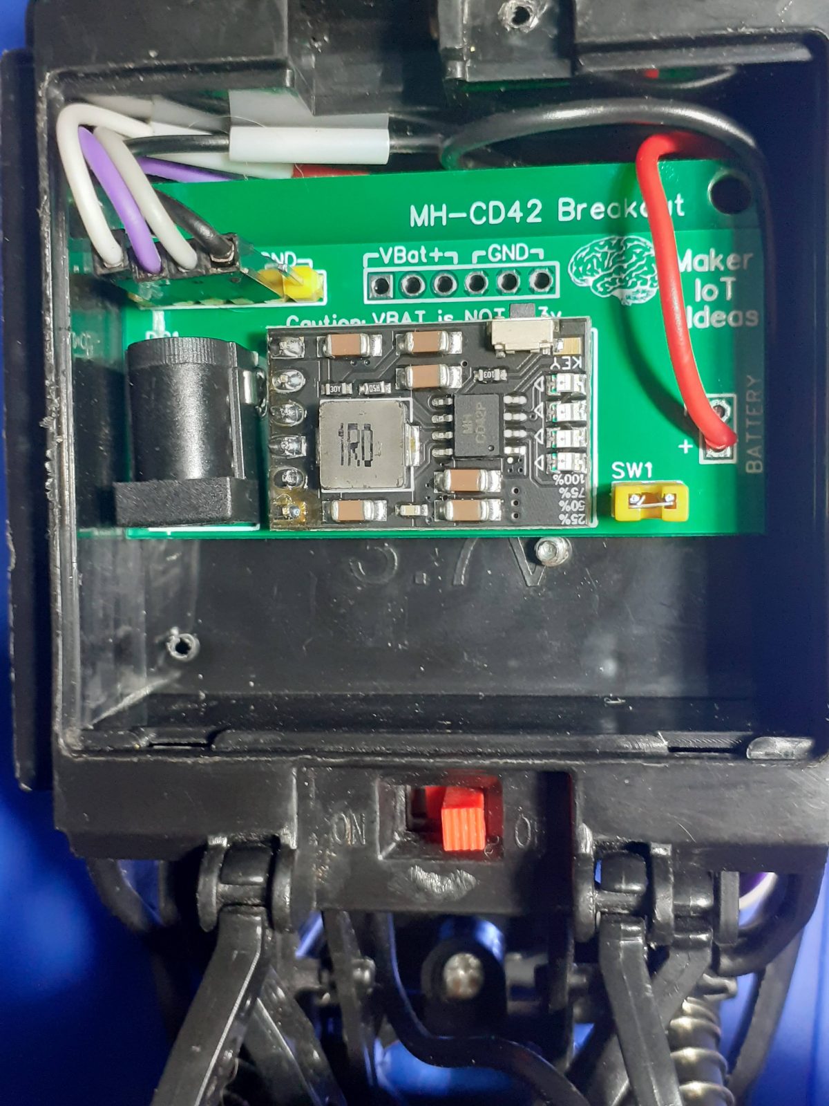
In this almost post we look at the power distribution PCB for the almost completed Robotic Toy Car. I had many interesting issues to solve here, especially since I did not design my own Lipo battery charger circuit, but used a very useful little commercially available unit instead, the MH-CD42
Based on a relatively difficult chip to get information on, the module is basically an integrated Lipo charge/discharge module, with a built-in boost converter that provides 5v at a maximum of 2A current. What makes it special is the ability to simultaneously provide current and voltage, as well as charge the attached LiPo cell at the same time, when connected to an external charger.
It does, however, in my view at least, also have a few serious flaws, the most irritating of these being that it will completely discharge the attached LiPo cell even when completely switched off…
I have thus tried to stop this issue from occurring by adding a switch in line with the Lipo Cell, a quite obvious solution, but it should not have been needed if the chip functioned as intended… ( As far as I can gather, the module was originally designed to be used in USB power banks. This makes the flaw even more serious, as a self-discharging power bank really defeats the purpose)
Enough of that though, when it does work, it works great. just remember that you can not apply more than 5.5v DC to the charging input of the module.
The completed Power Distribution and charging module
The Schematic
There is actually not a lot going on here, as everything is already on the supplied module. I have just added a charging port, additional power headers for 5v output and ground, as well as direct access to the LiPo Cell output, and a switch header to cut off power to the MH-CD42 when it is not in use.
The PCB
The PCB was manufactured as a 2-layer FR-4 board. The entire top layer is used as a ground plane, and the bottom layer was used for the 5v and Vbat traces, which were made as big as possible to allow for the high current ( up to 2A ) that the unit can supply to a load.
The TOP later of the PCB is a complete ground plane.The BOTTOM Layer caries only power traces for 5v and VBata 3D Render of the PCB, showing header pins and other connections
It is also worth mentioning that the VBAT pins are NOT 3.3v ( Remember that the LiPo cell can run from 4.2v down to 3.0v depending on the charge. These headers were only placed on the board to provide direct access to the LiPo cell, for use with for example an ADC input or for connection to a dev board that is already fitted with a buck converter or a suitable LDO voltage regulator.
The Actual PCB, as received from PCBWayTop Layer of the PCBBottom Layer of PCB
Manufacturing the PCB
Over the past eight years, PCBWay has continuously upgraded their MANUFACTURING plants and equipment to meet higher quality requirements, and now THEY also provide OEM services to build your products from ideas to mass production and access to the market.
The PCB for this project has been manufactured at PCBWay. Please consider supporting them if you would like your own copy of this PCB, or if you have any PCB of your own that you need to have manufactured.
If you would like to have PCBWAY manufacture one of your own, designs, or even this particular PCB, you need to do the following… 1) Click on this link 2) Create an account if you have not already got one of your own. If you use the link above, you will also instantly receive a $5USD coupon, which you can use on your first or any other order later. (Disclaimer: I will earn a small referral fee from PCBWay. This referral fee will not affect the cost of your order, nor will you pay any part thereof.) 3) Once you have gone to their website, and created an account, or login with your existing account,
4) Click on PCB Instant Quote
5) If you do not have any very special requirements for your PCB, click on Quick-order PCB
6) Click on Add Gerber File, and select your Gerber file(s) from your computer. Most of your PCB details will now be automatically selected, leaving you to only select the solder mask and silk-screen colour, as well as to remove the order number or not. You can of course fine-tune everything exactly as you want as well.
7) You can also select whether you want an SMD stencil, or have the board assembled after manufacturing. Please note that the assembly service, as well as the cost of your components, ARE NOT included in the initial quoted price. ( The quote will update depending on what options you select ).
8) When you are happy with the options that you have selected, you can click on the Save to Cart Button. From here on, you can go to the top of the screen, click on Cart, make any payment(s) or use any coupons that you have in your account.
Then just sit back and wait for your new PCB to be delivered to your door via the shipping company that you have selected during checkout.
In our last project, we started working on repurposing an old toy car. In this part, Robot Toy Car – The next steps, we will take a look at the controller board for this project and discuss some of the problems that we have encountered up to now. Most of the various components for this project are still in the prototype stage, but It is quite important to get them tested to verify the final designs.
There are quite a few unique challenges in a project like this, which looks quite easy to solve but turn out to become quite challenging to get working just right in practice…
One of the most important, as well as the most frustrating part, turned out to be the H-Bridge Motor controller. The first prototype of this was introduced in the first part of this project. While functional on paper, as well as working quite well in real life, (when tested with an Arduino, as well as manually), It performs extremely poorly when used with the actual controller for this project, an ESP8266 12-E…
What could the reason be? How will I fix it…? The answers to that will be provided in a follow-up post. For now, let us take a look at the controller.
The unassembled ESP-8266 Controller board, straight from the factoryThe Assembled ESP-8266 Controller board.
The Controller Board, details
Space inside the toy car is at a premium, so from the start, it was important to design a PCB that was small enough to fit, while also taking into consideration functionality, as well as all additional add-on components to ultimately be fitted to the project.
With this in mind, I have decided on the ESP-8266, which, while bigger than an Atmega328, does offer a few additional features, like WiFi, and ESP-Now, which will greatly help in controlling and even updating firmware OTA. The ESP-8266 does however also have a few serious flaws in this design, like limited useable GPIO pins, a 3.3v working voltage requirement, and quite high operating current requirements.
As the toy will likely not be used continuously, as well as the fact that it will run on batteries, which, can be replaced or recharged, I did not worry too much about the power issue. As far as the limited GPIO, that is where I2C comes in… It is quite easy to expand the GPIO with an IO Expander or two…
My main problem came in the form of the CH340G USB-to-UART converter chip. It seems like there must be quite a lot of counterfeit versions of these around, as none of the chips that I purchased, from many different suppliers, actually functioned, with the best one actually providing a USB port, but, when investigating with a logic analyser, the Rx and Tx lines of the UART, generating garbage…
Replacing it with a known working chip from a NodeMCU V1 board, magically solved the problem, verifying the PCB circuit as correct and working, and also proving that the purchased chips are definitely fake!
This was easily repaired by temporarily soldering jumper cables to the Rx and Tx lines on the ESP-8266, and using an external UART-to-USB converter to upload the initial sketch to the device. Future updates will be OTA, so not a problem in the long run anyway.
Controller Schematic
The controller schematic, above, is basically a rearranged stock NodeMCU v1 circuit, with the only difference being that only specific pins were broken out onto header pins. These will be used for controlling the two H-Bridges, and provide PWM as well as access to the I2C bus.
Software
Due to the fact that this controller is still definitely considered a prototype, my main focus is definitely on getting the control software sorted out first. That way, at least in my opinion, I can then focus on hardware issues responding to verified software inputs, without having to do both at the same time.
As mentioned before, I require OTA capability to upload new firmware to the device, so my starting point was the BasicOTA sketch provided with the Arduino IDE. This sketch was modified to perform some additional functionality, such as controlling the H-Bridges, PWM as well as a roof-mounted “status panel” with LED’s that also doubles as a visual display, to give a bit of colour to the project.
The “status panel” will be shown in a future post, however, with the only mention of it here being that it is I2C controlled, and based on a PCF8574.
The BasicOTA sketch is listed below.
#include <ESP8266WiFi.h>
#include <ESP8266mDNS.h>
#include <WiFiUdp.h>
#include <ArduinoOTA.h>

#ifndef STASSID
#define STASSID "your-ssid"
#define STAPSK  "your-password"
#endif

const char* ssid = STASSID;
const char* password = STAPSK;

void setup() {
  Serial.begin(115200);
  Serial.println("Booting");
  WiFi.mode(WIFI_STA);
  WiFi.begin(ssid, password);
  while (WiFi.waitForConnectResult() != WL_CONNECTED) {
    Serial.println("Connection Failed! Rebooting...");
    delay(5000);
    ESP.restart();
  }

  // Port defaults to 8266
  // ArduinoOTA.setPort(8266);

  // Hostname defaults to esp8266-[ChipID]
  // ArduinoOTA.setHostname("myesp8266");

  // No authentication by default
  // ArduinoOTA.setPassword("admin");

  // Password can be set with it's md5 value as well
  // MD5(admin) = 21232f297a57a5a743894a0e4a801fc3
  // ArduinoOTA.setPasswordHash("21232f297a57a5a743894a0e4a801fc3");

  ArduinoOTA.onStart([]() {
    String type;
    if (ArduinoOTA.getCommand() == U_FLASH) {
      type = "sketch";
    } else { // U_FS
      type = "filesystem";
    }

    // NOTE: if updating FS this would be the place to unmount FS using FS.end()
    Serial.println("Start updating " + type);
  });
  ArduinoOTA.onEnd([]() {
    Serial.println("\nEnd");
  });
  ArduinoOTA.onProgress([](unsigned int progress, unsigned int total) {
    Serial.printf("Progress: %u%%\r", (progress / (total / 100)));
  });
  ArduinoOTA.onError([](ota_error_t error) {
    Serial.printf("Error[%u]: ", error);
    if (error == OTA_AUTH_ERROR) {
      Serial.println("Auth Failed");
    } else if (error == OTA_BEGIN_ERROR) {
      Serial.println("Begin Failed");
    } else if (error == OTA_CONNECT_ERROR) {
      Serial.println("Connect Failed");
    } else if (error == OTA_RECEIVE_ERROR) {
      Serial.println("Receive Failed");
    } else if (error == OTA_END_ERROR) {
      Serial.println("End Failed");
    }
  });
  ArduinoOTA.begin();
  Serial.println("Ready");
  Serial.print("IP address: ");
  Serial.println(WiFi.localIP());
}

void loop() {
  ArduinoOTA.handle();
}
Controlling the Toy Car Robot
Controlling the Toy Car is a complicated question, with many ideas jumping into my mind, only to be pushed aside by technical issues, as well as real-world constraints on what is physically possible to be mounted on the plastic body of the toy car, space available on the inside, as well as not interfering with suspensions, springs, turning wheels etc.
The chassis of the toy car
As is clearly visible, there is really not a lot of space available here for sensors. Mounting sensors to the body will also provide a bit of a challenge, as well as won’t really look nice either…
I have thus decided to implement remote control for the time being, and later, maybe after 3d-printing a more suitable body, to add sensors for autonomous functionality. The ESP-Now protocol will be used extensively for the remote control, as, in my opinion, it required no additional hardware, is quite fast, as well as being extremely easy to use. It does however make it necessary to use another ESP deice in the remote control unit.
Manufacturing the PCB
The PCB for this project is currently on its way from China, after having been manufactured at PCBWay. Please consider supporting them if you would like your own copy of this PCB, or if you have any PCB of your own that you need to be manufactured.
If you would like to have PCBWAY manufacture one of your own, designs, or even this particular PCB, you need to do the following… 1) Click on this link 2) Create an account if you have not already got one of your own. If you use the link above, you will also instantly receive a $5USD coupon, which you can use on your first or any other order later. (Disclaimer: I will earn a small referral fee from PCBWay. This referral fee will not affect the cost of your order, nor will you pay any part thereof.) 3) Once you have gone to their website, and created an account, or login with your existing account,
4) Click on PCB Instant Quote
5) If you do not have any very special requirements for your PCB, click on Quick-order PCB
6) Click on Add Gerber File, and select your Gerber file(s) from your computer. Most of your PCB details will now be automatically selected, leaving you to only select the solder mask and silk-screen colour, as well as to remove the order number or not. You can of course fine-tune everything exactly as you want as well.
7) You can also select whether you want an SMD stencil, or have the board assembled after manufacturing. Please note that the assembly service, as well as the cost of your components, ARE NOT included in the initial quoted price. ( The quote will update depending on what options you select ).
8) When you are happy with the options that you have selected, you can click on the Save to Cart Button. From here on, you can go to the top of the screen, click on Cart, make any payment(s) or use any coupons that you have in your account.
Then just sit back and wait for your new PCB to be delivered to your door via the shipping company that you have selected during checkout.
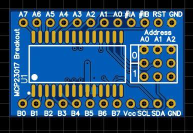
I2C port extenders or expanders are extremely useful devices, and I use quite a lot of them in my projects. My go-to device is definitely the PCF8574, mainly because it is sort of “breadboard friendly”. The MCP23017, with the existing breakouts available locally, are not. I have thus decided to design my own version of a breadboard friendly MCP23017 breakout board.
The Breakout Module PCB and its features
A breadboard friendly MCP23017 breakout board – Fronta breadboard friendly MCP23017 breakout board – Back
While this was definitely one of my easier projects, It still took a bit of time to get it just right and add some essential components and features directly onto the PCB.
The main features of this breakout: – DIP12 Layout – with all pins broken out, address pins to jumper headers… – Proper decoupling capacitors, as close as possible to the MCP23017 chip. I had to make use of the back layer of the PCB to do this, not exactly ideal, but with proper power and ground planes, and nice thick tracks, I believe they will be just fine.
– Address selector jumpers – The breakouts that are available locally, do not have these. – Breadboard friendly layout – 33.020mm x 20.320mm [board size], with 15.240mm vertical spacing between the rows of pins, ensures that you can easily fit it onto your breadboard, while still having space to add jumper wires to the pins. Horizontal pin spacing is standard 2.45mm.
The Schematic
The schematic is plain and simple. A few points to note though: – The address selection header, as well as the io pin headers are not shown on the schematic. – I2C pullup resistors are set at 1k but can be replaced with more suitable values as required in your circuit
The PCB for this project is currently on its way from China, after having been manufactured at PCBWay. Please consider supporting them if you would like your own copy of this PCB, or if you have any PCB of your own that you need to be manufactured.
If you would like to have PCBWAY manufacture one of your own, designs, or even this particular PCB, you need to do the following… 1) Click on this link 2) Create an account if you have not already got one of your own. If you use the link above, you will also instantly receive a $5USD coupon, which you can use on your first or any other order later. (Disclaimer: I will earn a small referral fee from PCBWay. This referral fee will not affect the cost of your order, nor will you pay any part thereof.) 3) Once you have gone to their website, and created an account, or login with your existing account,
4) Click on PCB Instant Quote
5) If you do not have any very special requirements for your PCB, click on Quick-order PCB
6) Click on Add Gerber File, and select your Gerber file(s) from your computer. Most of your PCB details will now be automatically selected, leaving you to only select the solder mask and silk-screen colour, as well as to remove the order number or not. You can of course fine-tune everything exactly as you want as well.
7) You can also select whether you want an SMD stencil, or have the board assembled after manufacturing. Please note that the assembly service, as well as the cost of your components, ARE NOT included in the initial quoted price. ( The quote will update depending on what options you select ).
8) When you are happy with the options that you have selected, you can click on the Save to Cart Button. From here on, you can go to the top of the screen, click on Cart, make any payment(s) or use any coupons that you have in your account.
Then just sit back and wait for your new PCB to be delivered to your door via the shipping company that you have selected during checkout.
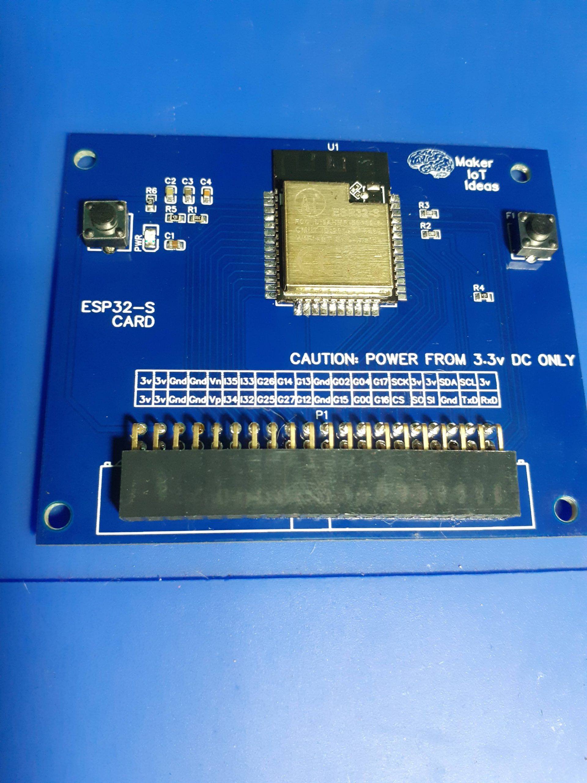
This project is the result of a lot of prototyping, using different MCUs and wanting to find a way to get a standard interface to all the devices.
The idea is to eventually create similar card-type MCU breakout boards, with similar pins in the same position on the 2x20p breakout header,
for example, power, i2c bus, reset and flash will always be in the same position on the female header…
Step 2 from here on would be to design a baseboard, that is capable of providing power, as well as access to the various GPIO pins. I am thinking along the way of a PC motherboard style interface, with “slots” at regular intervals. These “slots” will have access to the SPI, and I2C bus, as well as various other GPIO.
Step 3 would be a series of commonly used input and output “cards” that will plug into the “slots”…
If successful, I plan to design various MCU cards, with various different processors, with the obvious criteria that they are 3v powered.
This could result in a very flexible development platform, where it is possible to reuse the base-board and IO “cards” with any one of the various MCU “cards”.
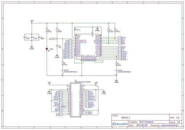
The Schematic
As seen on the schematic, almost all of the ESP32-S’s pins are broken out, with the exception of those used for internal flash. Reset and Flash circuitry is provided on the PCB, as well as on the 2x20pin female header.
It is worth noting that I did not include any UART to USB circuitry on the card. Flashing should be performed with an external USB-to-UART converter. It will however be included in the base-board.
There is also no power supply circuitry onboard. This was also intentional, as the card is intended to be powered from the base-board. It is however perfectly acceptable to power only the card from a suitable 3.3v DC power supply unit through the 3v and gnd pins on the 2x20pin header.
Where can I get my own version of this module?
This module will be exclusively available from PCBWay for the foreseeable future. Click on this link to order your own, and help support a great company that produces very high-quality PCBs for a very affordable price.
This PCB was manufactured at PCBWAY. The Gerber files and BOM, as well as all the schematics, will soon be available as a shared project on their website. If you would like to have PCBWAY manufacture one of your own, designs, or even this particular PCB, you need to do the following… 1) Click on this link 2) Create an account if you have not already got one of your own. If you use the link above, you will also instantly receive a $5USD coupon, which you can use on your first or any other order later. (Disclaimer: I will earn a small referral fee from PCBWay. This referral fee will not affect the cost of your order, nor will you pay any part thereof.) 3) Once you have gone to their website, and created an account, or login with your existing account,
4) Click on PCB Instant Quote
5) If you do not have any very special requirements for your PCB, click on Quick-order PCB
6) Click on Add Gerber File, and select your Gerber file(s) from your computer. Most of your PCB details will now be automatically selected, leaving you to only select the solder mask and silk-screen colour, as well as to remove the order number or not. You can of course fine-tune everything exactly as you want as well.
7) You can also select whether you want an SMD stencil, or have the board assembled after manufacturing. Please note that the assembly service, as well as the cost of your components, ARE NOT included in the initial quoted price. ( The quote will update depending on what options you select ).
8) When you are happy with the options that you have selected, you can click on the Save to Cart Button. From here on, you can go to the top of the screen, click on Cart, make any payment(s) or use any coupons that you have in your account.
Then just sit back and wait for your new PCB to be delivered to your door via the shipping company that you have selected during checkout.
Battery Backup for your Pi Zero (W) is a very important feature to prolong the life of the SD Card. Many commercially available solutions exist, in the form of Hats, but, unfortunately, it seems that anything that was specifically designed for the Raspberry Pi, can be quite expensive.
The 40 pin header on our Raspberry Pi Zero / Zero W gives us a lot of potentials to expand the functionality of this tiny single-board computer, but it, unfortunately, suffers from two major flaws, from my point of view of course.
The pins are scattered all over the place, and not grouped by function. Access to the pins is also very cluttered, to keep the overall footprint of the board small.
The GPIO pins are 3v only; adding anything that runs on a different voltage becomes a messy assembly of wires and level converters and or resistor dividers… going to a breadboard…
My Solution
Solving these issues required a lot of deep thinking, it actually took me a few months, during which I looked at various commercial solutions, imagined things in my mind, as well as tested concepts and various modules.
Let us take a look at some of these before I show you the solution that I am currently working on.
Battery Power
I would like to use a single 18650 LiPo cell to power the Pi Zero. Other Battery Backup solutions make use of this as well. In the ideal world, a pair of these in parallel would be great. The 18650 cell is a 3.3 volt ( nominal 4.2v) LiPo cell. The Pi needs 5v to run. This would require a Boost converter, as well as a dedicated LiPo charging circuit to recharge the cell after use.
Many such charging and Boost converters are available, but they seem to suffer from a problem, they need a dedicated charging cycle, during which using the device is not advised.
I could design my own circuit, but as I do not consider myself a proficient power supply designer, and with the huge amount of professionally designed, low-cost modules available, I decided to use the MH CD-42 module instead.
This module seems to give me all the features I need, with only one exception: The input voltage MUST be between 5.0v and 5.5v. I hope to address that issue later though.
It can source up to 2A at 5v, and most importantly, has a current bypass function, which allows you to charge the battery, as well as power an external device at the same time.
GPIO Pin Grouping and Level Conversion
The next logical step was to design a base-board that contained the 18650 Cell, and power module, as well as provide access to the GPIO pins.
I decided to use a 90 degree 2×20 pin Female header to mount the Pi, allowing for plenty of airflow around it to prevent overheating, as well as clearly labelled header pins for access to the GPIO pins. ( Due to logistics issues, the female header pin has not arrived yet).
The logic level conversion was provided on some of the GPIO ( SPI0, SPI1, I2C and UART ) by using the TXS0108E 8Ch Bidirectional Level Shifter chip from TI. Headers in black are 3v ( with exception of GPIO13) and 5v logic pins are on a white header.
Additional Ground and Power headers for 5v and 3v (red headers) were also added. Finally, a dedicated shutdown button was connected to GPIO26.
Schematic
Testing the prototype
The prototype is still under testing, as mentioned above, I still have to receive the 40 pin female header. I did however connect the Pi Zero to the board with jumper wires ( 3v, 5v and ground only ) to test operation. So far, the setup provides 5 hours of battery backup with the Pi on idle, no external devices connected and running only an MQTT server on Raspberry Pi Lite OS ( No Gui )
The first revision of the device is available for order at PCBWay
Manufacturing the PCB
This PCB was manufactured at PCBWAY. The Gerber files and BOM, as well as all the schematics, will soon be available as a shared project on their website. If you would like to have PCBWAY manufacture one of your own, designs, or even this particular PCB, you need to do the following… 1) Click on this link 2) Create an account if you have not already got one of your own. If you use the link above, you will also instantly receive a $5USD coupon, which you can use on your first or any other order later. (Disclaimer: I will earn a small referral fee from PCBWay. This referral fee will not affect the cost of your order, nor will you pay any part thereof.) 3) Once you have gone to their website, and created an account, or login with your existing account,
4) Click on PCB Instant Quote
5) If you do not have any very special requirements for your PCB, click on Quick-order PCB
6) Click on Add Gerber File, and select your Gerber file(s) from your computer. Most of your PCB details will now be automatically selected, leaving you to only select the solder mask and silk-screen colour, as well as to remove the order number or not. You can of course fine-tune everything exactly as you want as well.
7) You can also select whether you want an SMD stencil, or have the board assembled after manufacturing. Please note that the assembly service, as well as the cost of your components, ARE NOT included in the initial quoted price. ( The quote will update depending on what options you select ).
8) When you are happy with the options that you have selected, you can click on the Save to Cart Button. From here on, you can go to the top of the screen, click on Cart, make any payment(s) or use any coupons that you have in your account.
Then just sit back and wait for your new PCB to be delivered to your door via the shipping company that you have selected during checkout.
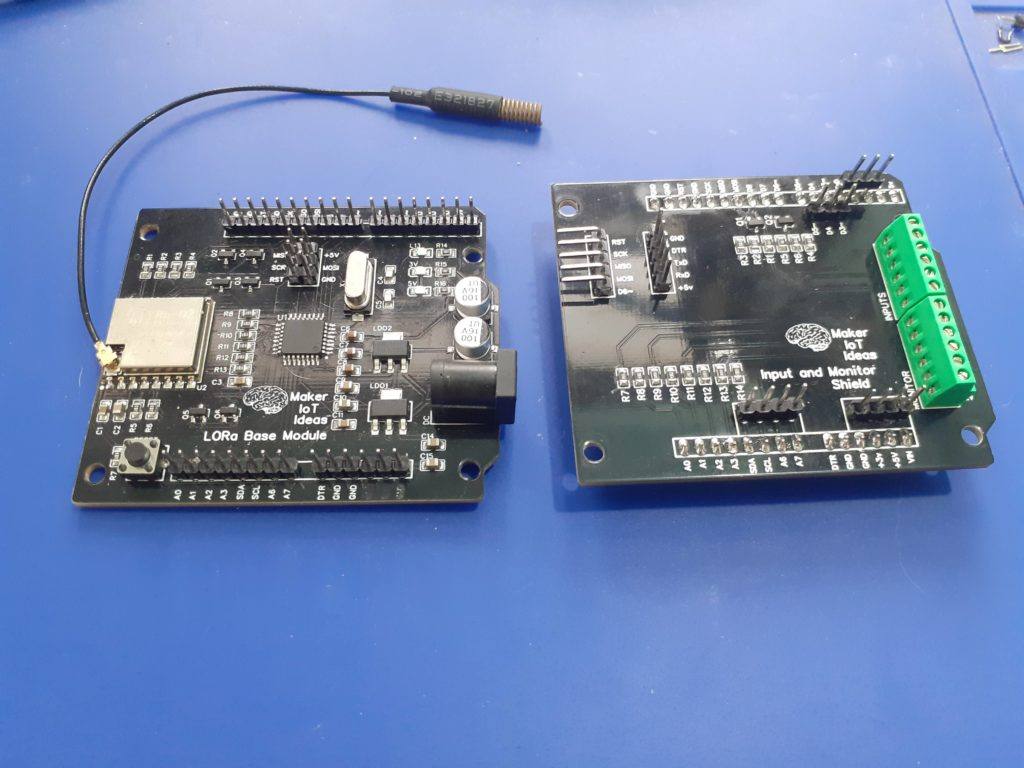
This is a straightforward project compared to my usual PCB projects. It is one of a series of designs towards completing my LoRa monitoring system, that I plan to use on the farm to monitor various areas, such as intrusion detection, battery levels etc.
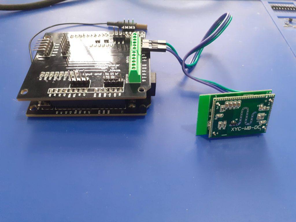
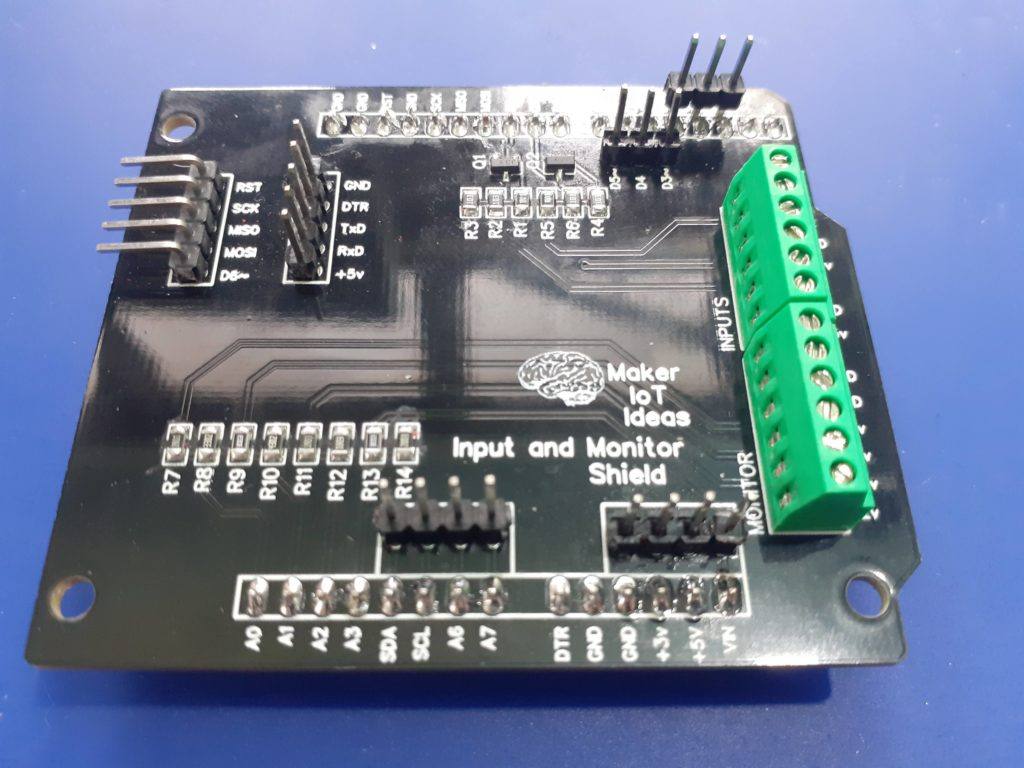
The shield was designed to fit on top of the first LoRa Base Module. It was designed to allow easy, neat connections to Infrared Beam sensors, XYC-WB-DC Motion Detector, as well as to monitor the battery levels at the Solar power inverter (the farm is completely off-grid).
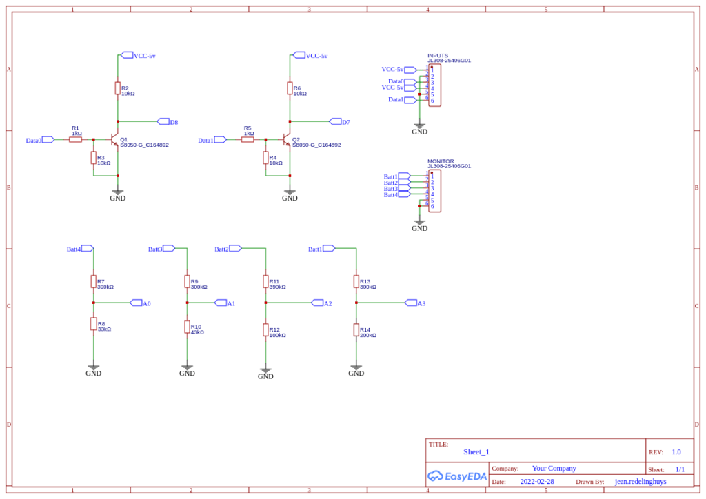
The Motion Sensor provides a +3v signal that goes high on motion detection, while the Infrared Beam Sensor provides a relay contact that can be used to provide a similar voltage signal. As I prefer to use pull-up logic on my inputs, I decided to implement a simple transistor circuit where the input will switch the base of the transistor, which in turn will pull the input to signal ground when switched on. This circuit uses the S8050 transistor, with the base pulled down to signal ground via a 10k resistor to prevent floating, and a current limiting resistor of 1k to 1k8 on the base. The collector, as well as the D7 and D8 GPIO pins on the LoRa Base Module, is pulled High to Vcc5v via a 10k resistor.
Voltage monitoring is done with the ADC on the LoRa Base Module, with each of the 4 battery levels ( 12v, 24v,36v, and 56v) being connected to the relevant ADC channel via a resister-divider network to lower the respective voltage to a level between 0 and 5v. ( This was done as the ADC on the ATMEGA328p can only handle a maximum voltage of 5.0v )
The resistors were chosen to give a slightly bigger input voltage range, to accommodate for fluctuations from the solar charger ( It can sometimes go up to 65v on a very bright sunny day ). I decided to not add any current limiting resistors directly onto the PCB, as they are definitely going to be bulky. They will instead be attached externally, to suitable heatsinks, etc…
As this PBC is still in the prototype stage, and my LoRa Monitoring device will definitely go through quite a few modifications in future, I provided access to all unused GPIO pins via separate headers on the shield. Most notably the SPI Header, used for programming the ATMEGA328P MCU, or connecting other SPI devices ( I am working on a CAN bus addon for the device, to save on the number of physical radio nodes that needs to be installed), The UART Header, as well as I2C, A6, A7 and additional Digital IO Pins (D3~, D4, D5~).
In the photo above you will notice an additional header on the UART pins, This was added to assist me with debugging on the logic analyser, as I had a slight issue with waking up the ATMEGA328P, and getting it to send events via LoRa. It would wake up, print status messages through the UART, but never do the actual LoRa part! That has now been fixed, and the header removed…
The schematic diagram for the shield is below. As you will see, it is very uncomplicated indeed.
The RA-02 Module (SX1278) connections to the ATMEGA328p is as follows:
NSS to D10 (CE)
MOSI to D11 (MOSI)
MISO to D12 (MISO)
SCK to D13 (SCK)
RESET to D9
DIO0 to D2 ( We need a hardware Interrupt pin ).
DIO1 to DIO5 was not broken out on the current version of the LoRa Base Module
There is also no direct access to pins D10, D9 and D2 either on the LoRa Base Module or on the Input and Monitor Shield.
If you do decide to hack the device and add access to any of the non broken out pins, please remember to use a logic level converter between the ATMEGA328 and the SX1278, as they operate at different voltages, and the SX1278 is not 5v tolerant on any of the IO Pins!
You can order this shield from PCBWay by clicking here
This PCB was manufactured at PCBWAY. The Gerber files and BOM, as well as all the schematics, will soon be available as a shared project on their website. If you would like to have PCBWAY manufacture one of your own, designs, or even this particular PCB, you need to do the following… 1) Click on this link 2) Create an account if you have not already got one of your own. If you use the link above, you will also instantly receive a $5USD coupon, which you can use on your first or any other order later. (Disclaimer: I will earn a small referral fee from PCBWay. This referral fee will not affect the cost of your order, nor will you pay any part thereof.) 3) Once you have gone to their website, and created an account, or login with your existing account,
4) Click on PCB Instant Quote
5) If you do not have any very special requirements for your PCB, click on Quick-order PCB
6) Click on Add Gerber File, and select your Gerber file(s) from your computer. Most of your PCB details will now be automatically selected, leaving you to only select the solder mask and silk-screen colour, as well as to remove the order number or not. You can of course fine-tune everything exactly as you want as well.
7) You can also select whether you want an SMD stencil, or have the board assembled after manufacturing. Please note that the assembly service, as well as the cost of your components, ARE NOT included in the initial quoted price. ( The quote will update depending on what options you select ).
8) When you are happy with the options that you have selected, you can click on the Save to Cart Button. From here on, you can go to the top of the screen, click on Cart, make any payment(s) or use any coupons that you have in your account.
Then just sit back and wait for your new PCB to be delivered to your door via the shipping company that you have selected during checkout.
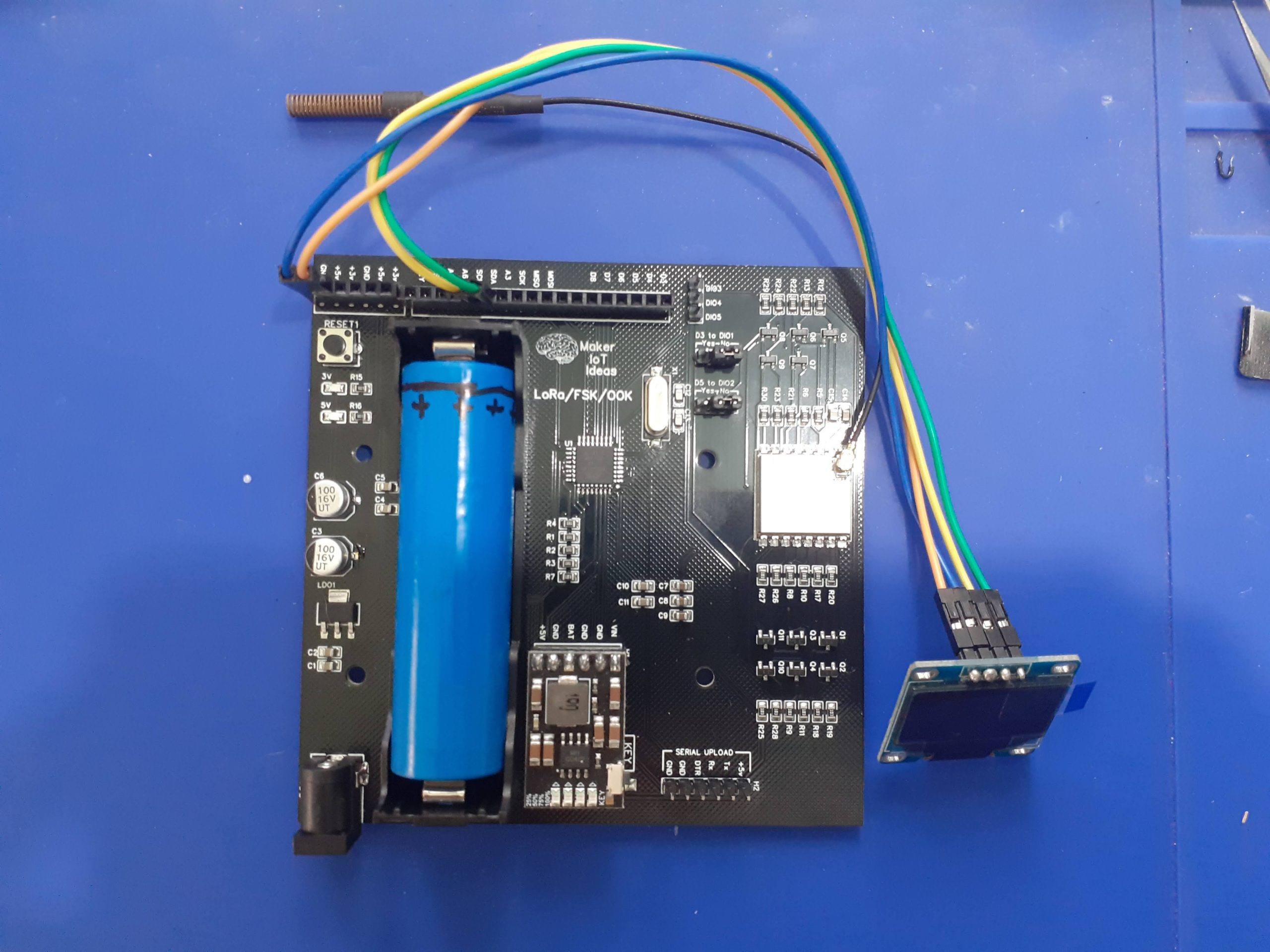
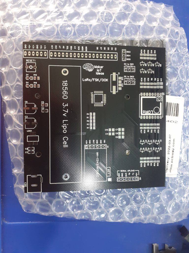
SX127x LoRa/FSK/OOK Module with LiPo battery-backup
SX127x LoRa/FSK/OOK Prototype Radio Board
I recently had a requirement to do some automation/telemetry on the farm. Things went missing, unauthorised persons were trespassing on the property, helping themselves to eggs, chickens, ducks and produce. Something had to be done, and as there is nobody sleeping there at night, it had to be possible to get remote status updates in real-time.
The farm is also completely off-grid, with solar-powered inverters taking care of all the water and electricity needs. Power usage monitoring could thus be a great help as well…
The idea is as follows:
Have a central control station, with various remote devices to do intrusion detection, control lights and water pumps, as well as monitor the battery levels of the inverter and solar-panel system. As the area is quite large, having to pull in electrical cabling will not be feasible, nor could the inverter handle all of that.
I decided to use the RA-02 LoRa/FSK/OOK module, on a custom PCB, but with various different PCB modifications, to take care of each stage of the project. The PCB that I will present today will be mainly used as the control unit, but it could also be a remote station, depending on what options are needed.
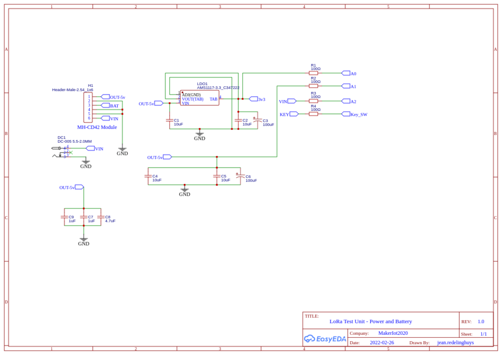
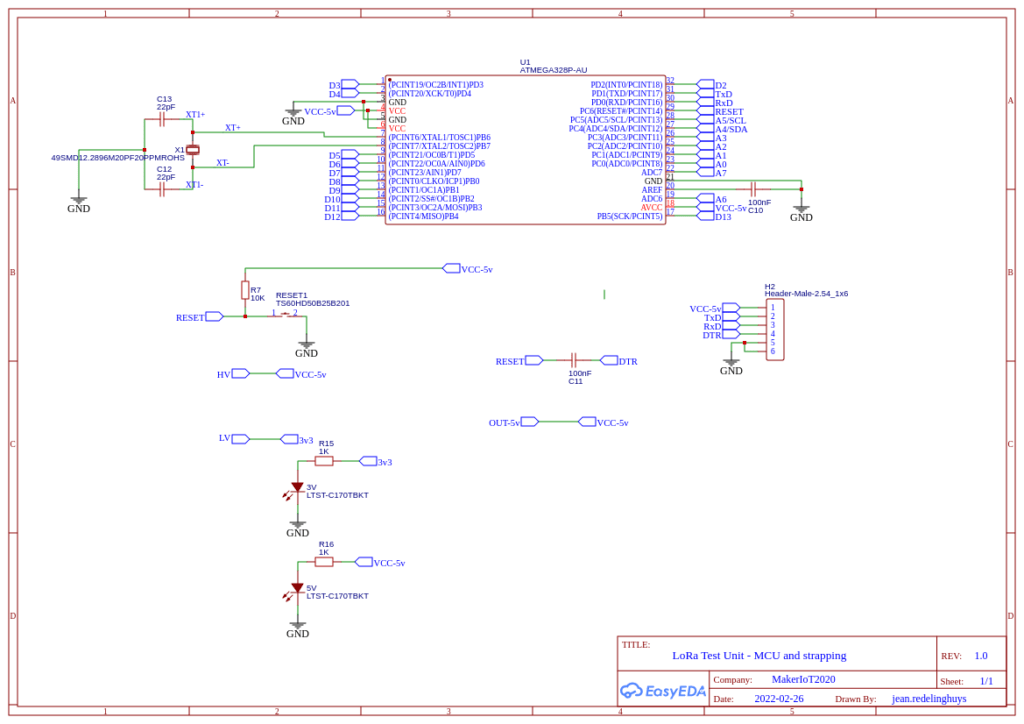
The ATMEGA328P-AU MCU is used as the main processor on each board, with the MH-CD42 Boost Converter/LiPo battery charger module taking care of power supply requirements. This module can source up to 2A at 5.0v, More than adequate for my needs. The ATMEGA328P will be put into sleep mode, to wake on interrupt to respond to events as needed ( To help save power ). Power usage of the circuit is around 50mA in standby ( NOT SLEEP MODE ), and with a peak of 100mA on a LoRa Transmit or Receive event.
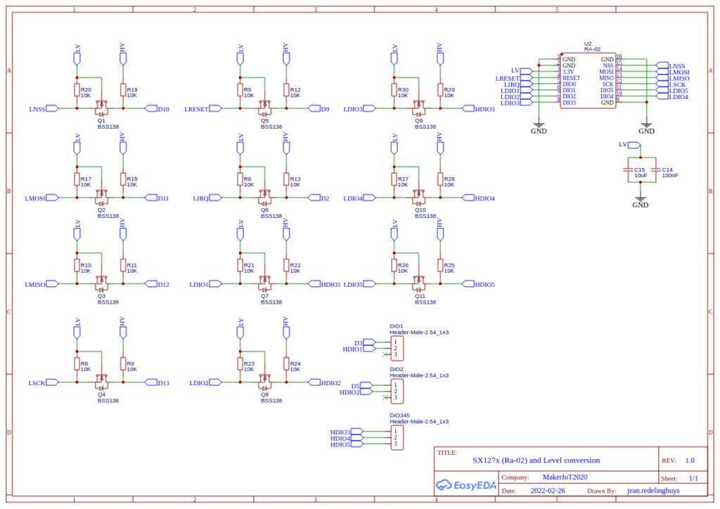
The RA-02 Module did however present some challenges, as it is a 3.3v device, with non-5v capable IO lines. This made it necessary to include a 3.3v LDO regulator, as well as logic level converting circuitry onto the PCB. To allow for the most flexibility, all DIOs on the RA-02 was also broken out via level converters, in addition to the required SPI pins ( MOSI, MISO, CE and SCK ). This amount to a total of 11 level converters onboard.
I chose the MH-CD42 Power module for the reason that it can supply current at the same time as charging the LiPo battery (in my case, I used a 18650 cell). This will help greatly, as 220v inverter power is available during the day to charge the batteries.
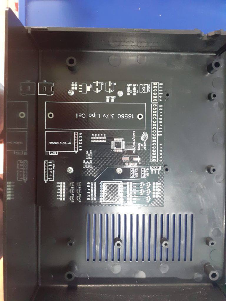
Another challenge was definitely the enclosure. I found some really nice enclosures online, but the mounting holes were located in a very particular pattern, making it necessary to do some very careful measuring to get the PCB to fit exactly. The enclosure also has space to accept the other PCB modules, like the USER Control panel, and other sensor devices as needed. PCBWay did a great job at manufacturing the PCB so as to fit exactly. I must admit that I had quite a few tense moments between sending the PCB off to manufacturing and receiving it, as to whether my measurements were actually accurate, and if the PCB would fit as I imagined…
As you can see in the picture above, it turned out perfectly.
The Circuit diagram is basically a standard Arduino Nano ( I needed access to all of the ADC pins ),
Connections to the RA-02 module is as follows:
RA-02
ATMEGA328P
MOSI
D11
MISO
D12
SCK
D13
CE
D10
RESET
D9
DIO0
D2 ( We need a hardware interrupt pin here )
DIO1
D3 ( Hardware Interrupt, enabled through jumper)
DIO2
D5 ( Enabled through a jumper)
DIO3 to DIO 5
Not connected, available on a breakout header
Connections between Ra-02 (SX127x) and ATMEGA328P – Note that all IO Lines are connected through level converters 5v <-> 3.3v
On the ATMEGA328, the following pins are broken out into headers:
D3
can be connected to RA-02 with a jumper
D4
D5
can be connected to RA-02 with a jumper
D6
D7
D8
D13 ( SCK )
Broken out as a 5v logic pin
D12 ( MISO )
5v logic pin
D11 ( MOSI )
5v logic pin
A3,A6,A7
ADC Pins ( A0, A1, A2 is used internally to monitor VIN, VCC5v and VCC3v ) A0 = Vcc3v A1 = Vcc5v A2 = VIN
SCL
I2C SCL pin OR A5 (I2C pins are at 5v logic levels )
SDA
I2C SDA pin OR A4 (I2C pins are at 5v logic levels )
RESET
DTR
( connected through a 100nf Cap to Reset, used for serial uploading firmware )
D0 ( RxD )
UART Rx Pin ( 5v logic )
D1 ( TxD )
UART Tx Pin ( 5v logic )
ATMEGA328P breakout pins. All pins are at 5v logic level
The ATMEGA328P is clocked at 16Mhz through an external crystal.
3v, 5v and GND pins were broken out at two opposite corners of the PCB to allow easy connection of additional devices/ sensors as needed.
The MH-CD42 module has the capability to power a load while charging the LiPo battery. This makes it possible to do a few interesting things while supplying power to this particular PCB.
The board can be powered directly from a 5v header pin ( NOT from the DC1 input ). In this mode, a LiPo battery is not required.
5v will be directly supplied to the processor, as well as the 3.3v LDO regulator, allowing the RA-02 module to function as well.
PLEASE NOTE: THERE ARE NO 5v REGULATION – MAKE SURE YOU SUPPLY REGULATED 5v
Installing the MH-CD42 module will add the option of charging a 3.3v 18650 Lipo battery, as well as powering the board at the same time. You need to supply power through the DC plug to make use of this function. This mode is also a miniature uninterruptible power supply, with the 3.3v LiPo battery immediately taking over should the main DC input fail.
NOTE: The MH-CD42 can only accept up to 5.5v MAXIMUM as input!
Software:
The PCB can be used with LoRa libraries from Sandeep Mistry OR JGromes/RadioLib ( If you want to do FSK/OOK or other advanced stuff like LoRa of FHSS)
Both libraries have extensive examples showing how to use them. As our use case will definitely differ, I will not have any example here at this stage. I will add one later after the entire project is completed, with all the relevant modules.
This PCB was manufactured at PCBWAY. The Gerber files and BOM, as well as all the schematics, will soon be available as a shared project on their website. If you would like to have PCBWAY manufacture one of your own, designs, or even this particular PCB, you need to do the following… 1) Click on this link 2) Create an account if you have not already got one of your own. If you use the link above, you will also instantly receive a $5USD coupon, which you can use on your first or any other order later. (Disclaimer: I will earn a small referral fee from PCBWay. This referral fee will not affect the cost of your order, nor will you pay any part thereof.) 3) Once you have gone to their website, and created an account, or login with your existing account,
4) Click on PCB Instant Quote
5) If you do not have any very special requirements for your PCB, click on Quick-order PCB
6) Click on Add Gerber File, and select your Gerber file(s) from your computer. Most of your PCB details will now be automatically selected, leaving you to only select the solder mask and silk-screen colour, as well as to remove the order number or not. You can of course fine-tune everything exactly as you want as well.
7) You can also select whether you want an SMD stencil, or have the board assembled after manufacturing. Please note that the assembly service, as well as the cost of your components, ARE NOT included in the initial quoted price. ( The quote will update depending on what options you select ).
8) When you are happy with the options that you have selected, you can click on the Save to Cart Button. From here on, you can go to the top of the screen, click on Cart, make any payment(s) or use any coupons that you have in your account.
Then just sit back and wait for your new PCB to be delivered to your door via the shipping company that you have selected during checkout.