`Ai-Thinker (#notsponsored) should be quite well known to many makers as a company that manufactured and designs many of the modules that we use in our projects. We, MakerIoT2020, definitely make use of quite a few of their products, like the RA-02, as well as their ESP32-S module.
A few months ago, I got the opportunity to play with one of their newest projects, the AI-WB2, which is based on the BL602 Risc-V Chip. After a very very bumpy ride, mainly due to the chip being quite new, and documentation being virtually nonexistent in the English language, I decided to take a step back, and stop trying to reinvent the wheel 🙂 Afterall, I don’t want to use Apache NuttX or a similar RTOS for every project, as the thought of having to write almost all of the different required components from scratch, does not really appeal to me. especially as the SDK is in Chinese, and the English version of it is a bit patchy, to say the least…
This made me quite a bit frustrated, at least until I decided to change my thinking, and take a look at the stock AT command set that comes shipped on the modules from the factory… While excellent for use as a WiFi modem, it did not seem to allow any access to any of the GPIO on the WB-AI2 module… But wait… is that really a problem? No… Let me tell you why…
A few very quick tests later, It was clear that the AI-WB2 will be a very compact WiFi as well as BTLE connectivity solution for these XIAO modules, and, If I design with the future in mind, the GPIO pins of the AI-WB2 module can also become useable to me as well… once the firmware and SDK gets more accessible..
What followed from this is a very basic prototype PCB, with the XIAO RP2040 as the main processor, and the AI-WB2-12F as a “connectivity co-processor”, meaning that all communications functions will be offloaded to the AI-WB2 and the results of those, sent back to the XIAO for processing…
This in itself presents quite a few challenges, especially on the communications handling, and using the second UART port, which is currently not possible with the official Arduino Core for the RP2040… Luckily, the XIAO RP2040 uses an alternative core, that supports the second UART port quite well …
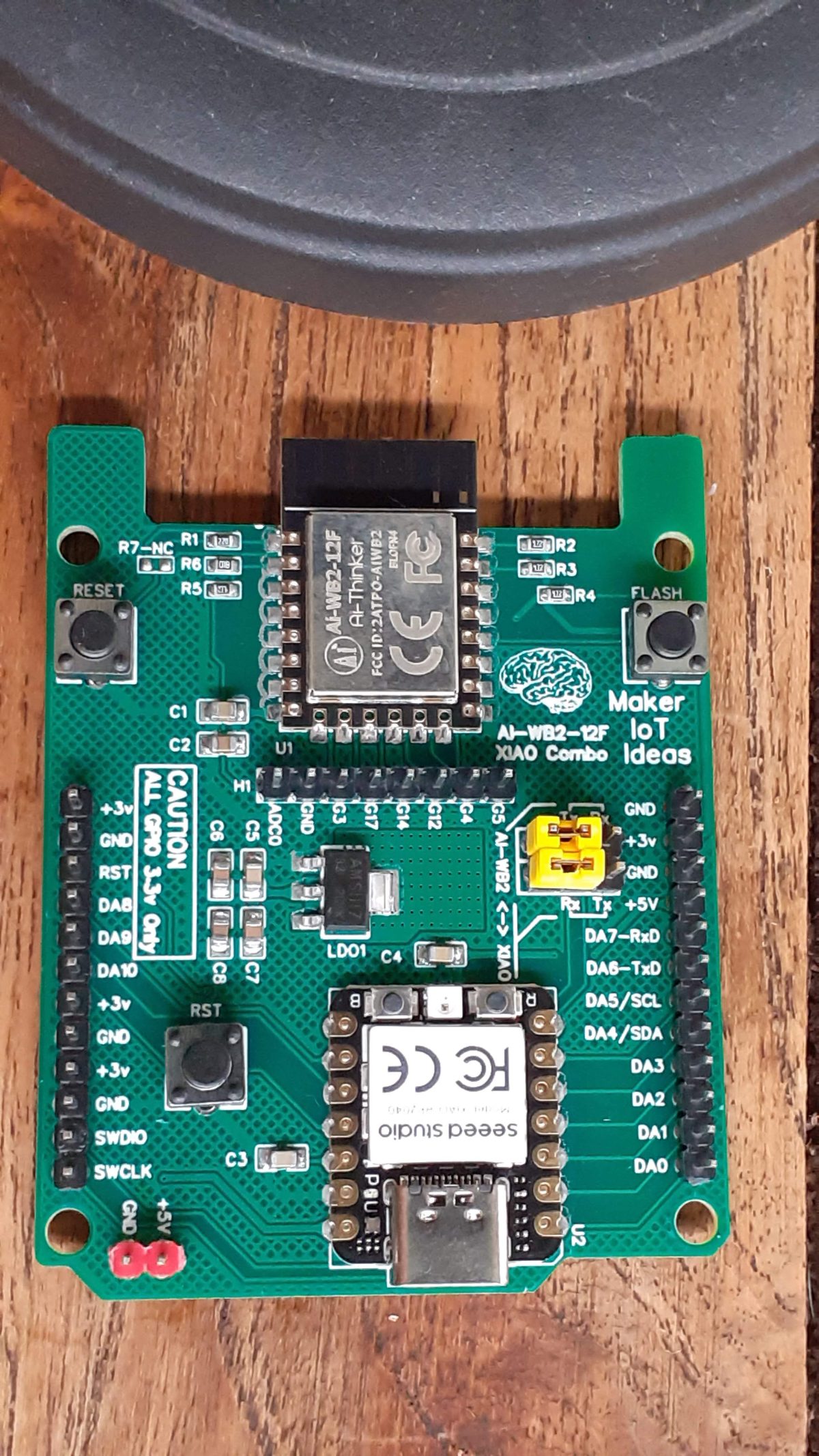
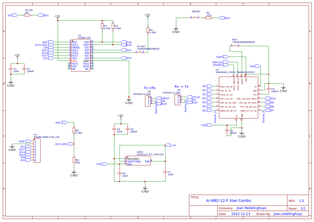
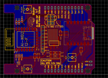
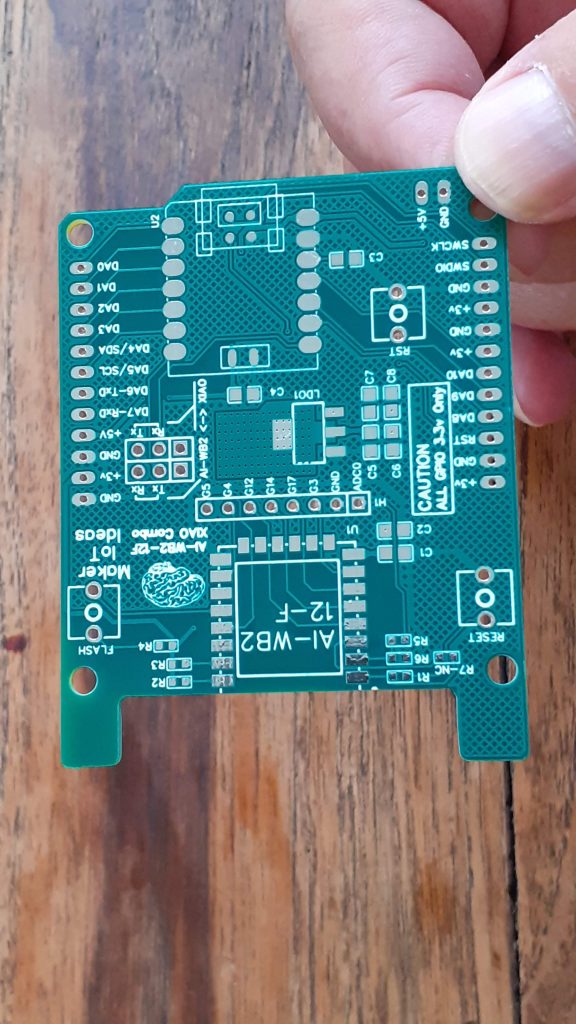
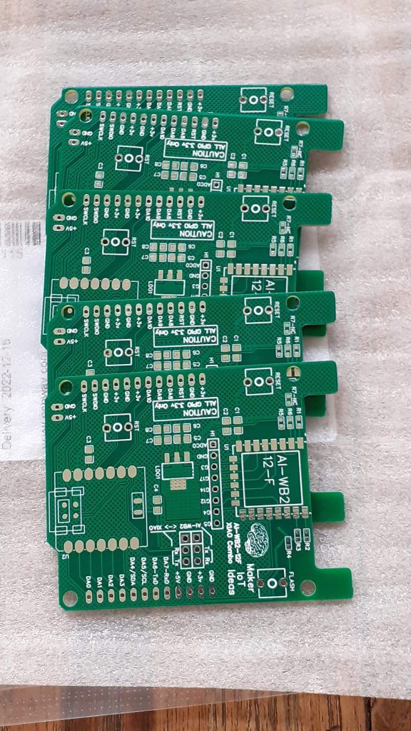
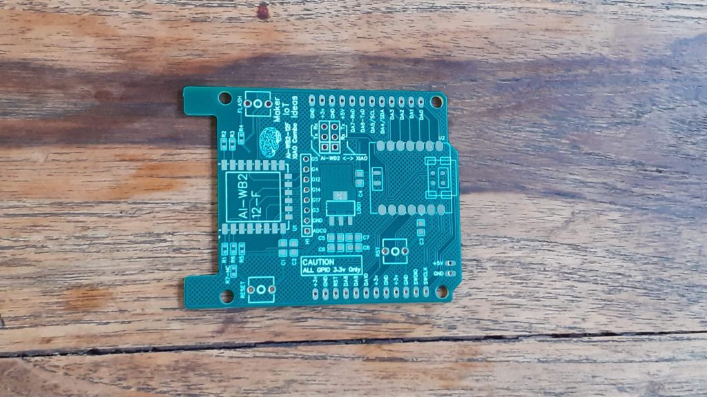
What is on the PCB?
AI-WB2-12F XIAO Combo
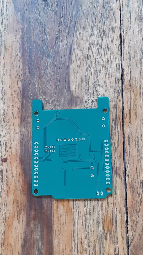
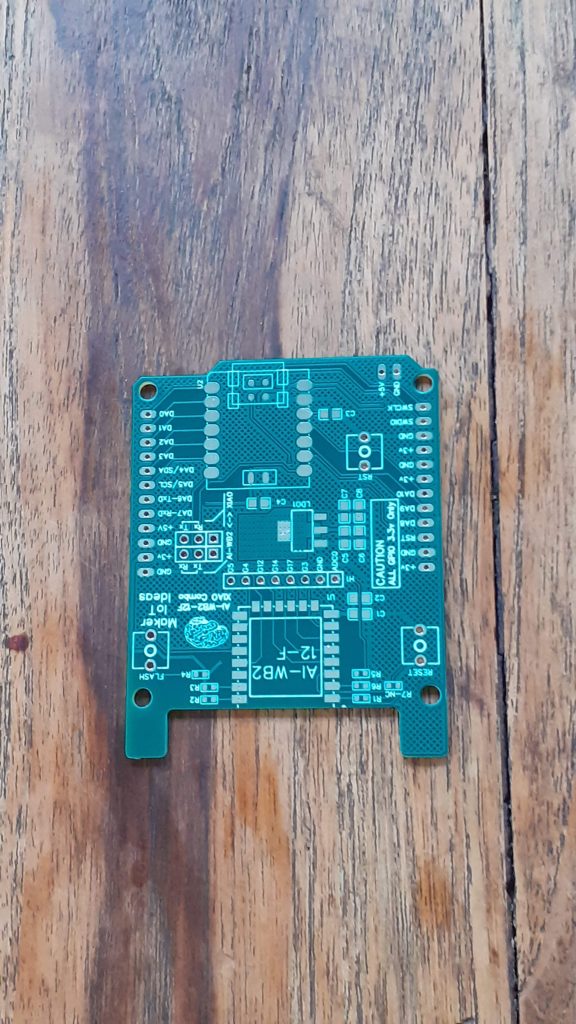
The Top Section of the PCB is dedicated to the AI-WB2-12F and its supporting components, including a flash and reset button. The GPIO for the WB2-12F is broken out onto H1.
At the right, below H1, is a series of jumpers, connecting the Xiao RP2040 and WB2-12-F Uart ports, or, alternatively, connecting the XIAO Rp2040 to the pin headers at the side of the PCB.
The rest of the PCB is dedicated to the Xiao RP2040 or Xiao SAMD21 module, with its supporting circuitry, and a dedicated Reset button for the SAMD21 module ( also works for the RP2040)
The board is powered with 5v DC through a dedicated header at the left bottom. This directly powers the Xiao and indirectly powers the WB2-12-F through a 3.3v LDO Regulator. Please note that although the Xiao is powered via 5v, the GPIO pins are all 3.3v logic!
For the Xiao RP2040, like I used, it is possible to use the second UART to connect to the AI-WB2 chip.
As I am still not completely done with my development, I will not release the full code at this moment.
I have also been informed by AI-Thinker that a new version of the AT-command firmware is available that will allow using the GPIO on the AI-WB2 via AT Commands. I am currently investigating that new version, and that is also a big reason for not releasing any code at this stage.
Manufacturing
The PCB for this project has been manufactured at PCBWay. Please consider supporting them if you would like your own copy of this PCB, or if you have any PCB of your own that you need to have manufactured.
These days, Makers have access to quite a few different microprocessors for use in their projects. Most of them can be found on development boards of some sort, but not all are in a convenient size. The reason for this is that most of these development boards were designed with a breadboard in mind, and then after your prototype is done, you are required to design a PCB and place the specific processor and its supporting components onto this custom PCB…
Many makers choose to skip this step, either choosing to keep the project on the breadboard, or place the entire development module onto a piece of stripboard or similar, and then place their supporting components and sensors around that.
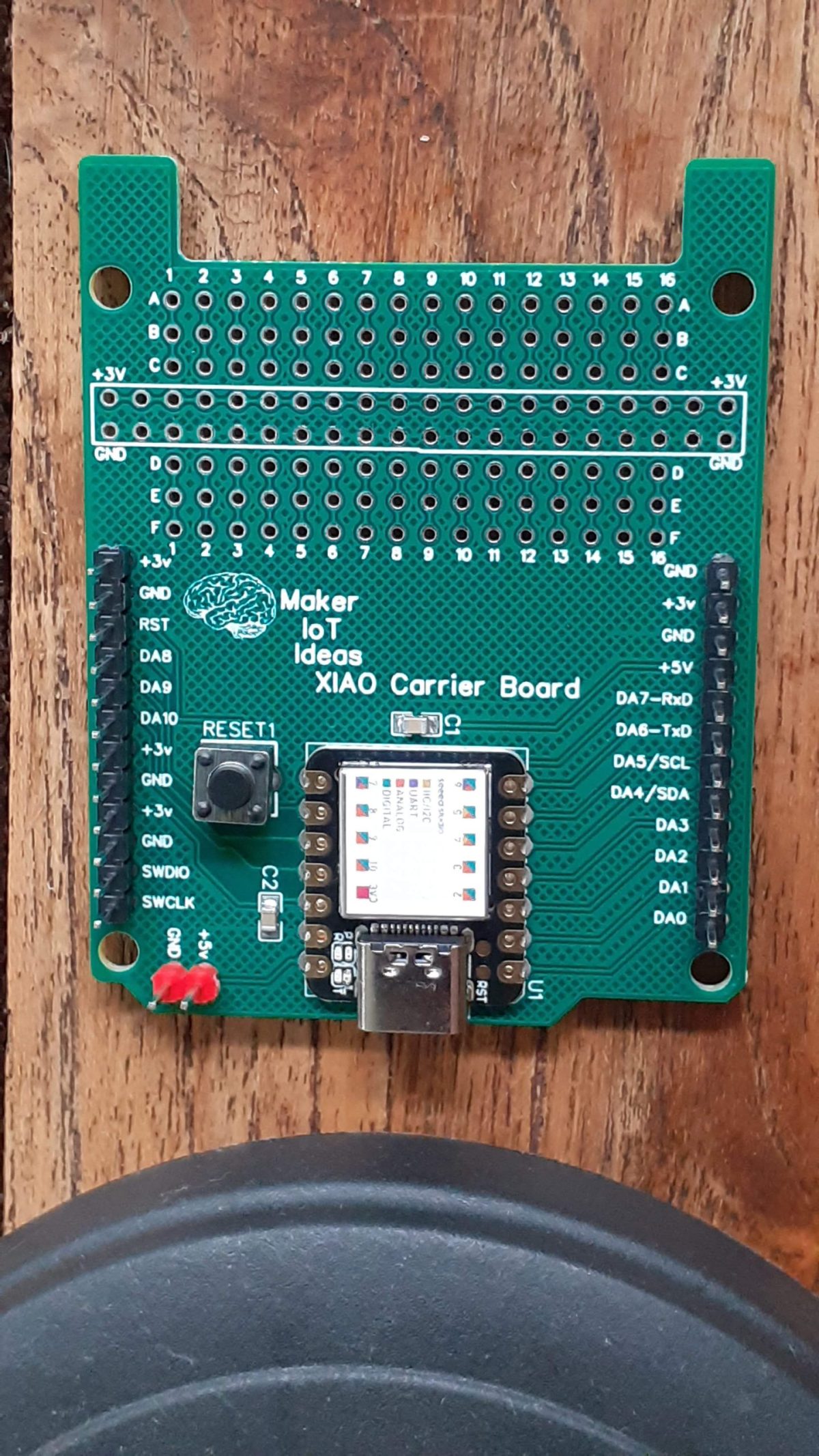
This is where the SEEED XIAO is different. It comes in a thumb-nail-sized package and can be used on the breadboard or directly placed onto a PCB via either pin headers or if you want access to all of its features, SMD pads.
I have also included a small prototype area on the PCB, so that Makers can easily transfer their existing XIAO projects onto a semi-custom PCB, without having to design their own.
I have also addressed a problem area, especially with the XIAO SAMD21, it has no onboard reset button, only two tiny pads, by including a reset button for ease of use.
The PCB is in Arduino Uno form factor, and also provides headers to power it from an external 5v DC supply. Please note that the prototyping area has a 3.3v power rail, – due to the fact that all of the XIAO GPIO are limited to 3.3v anyway -. This power rail is powered directly from the XIAO 3.3v output, and the current is limited as per the specifications of the XIAO module that you are using.
The PCB for this project has been manufactured at PCBWay. Please consider supporting them if you would like your own copy of this PCB, or if you have any PCB of your own that you need to have manufactured.
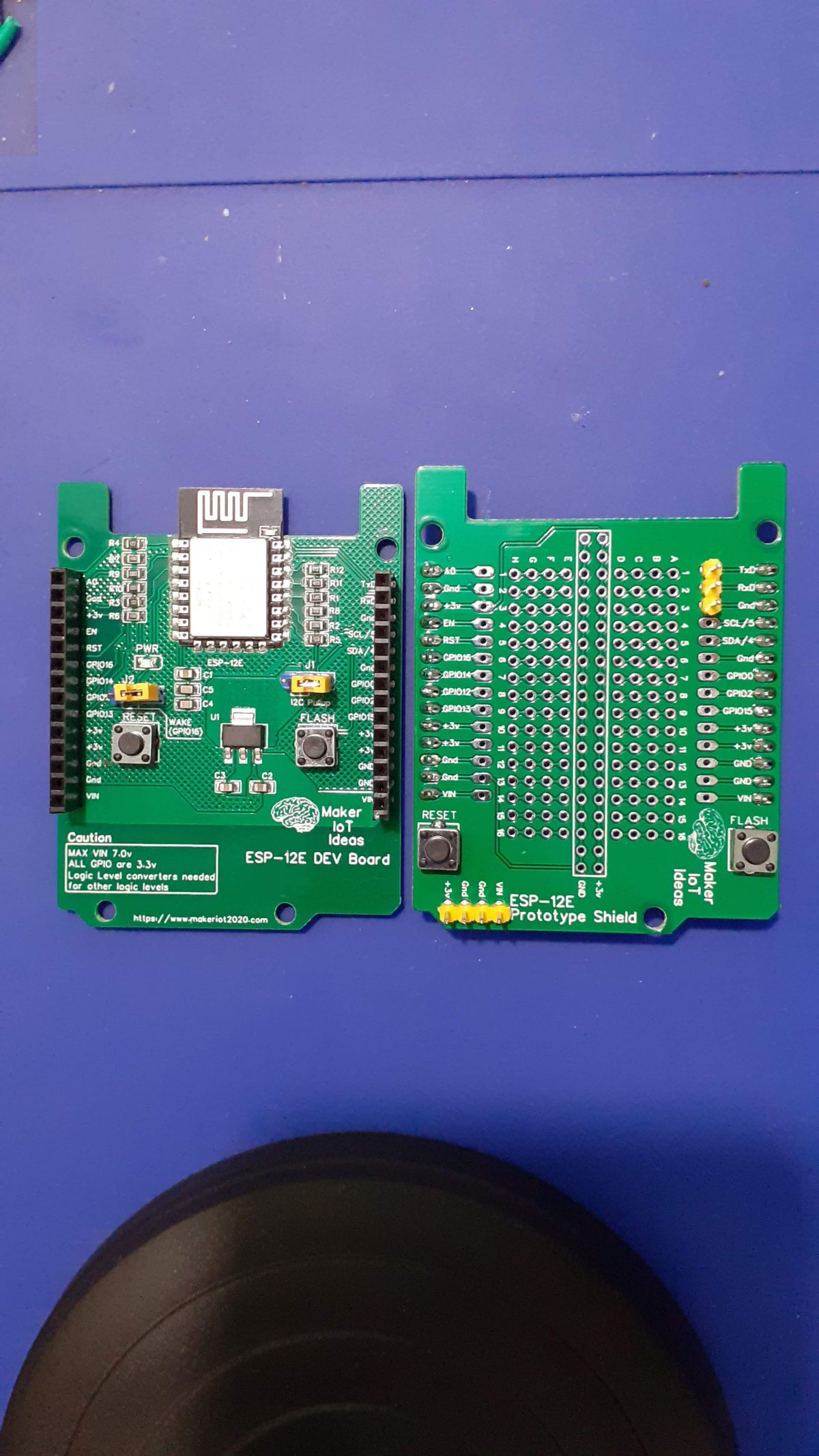
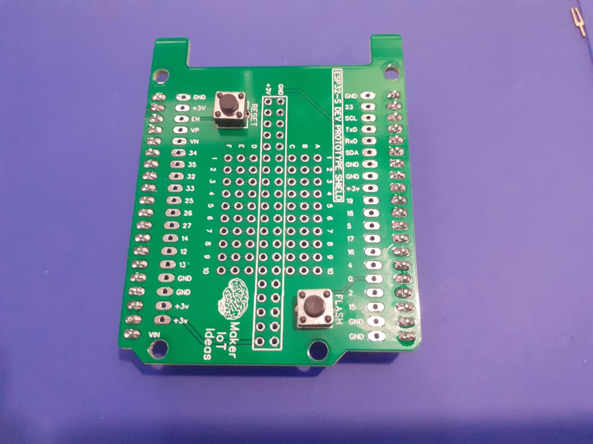
In answer to quite a few requests for a prototype shield, similar to my ESP32-S Dev Prototype shield, but for use with the ESP-12E DEV board, I have decided to do a quick design, and make it available publicly
This is the MakerIOT2020 ESP12E-DEV Prototype Shield. It is similar in purpose to the above-mentioned ESP32-S Dev Prototype shield, but I have also added some additional cosmetic changes to make it a little easier to use as well.
With many of my prototype designs, I tend to sometimes leave out something, as I usually use it for my own purposes only, but with this design, as many people specifically asked for it, I took a bit more care, as it is no longer just a prototype, right?
What has changed?
The most obvious is the increased prototyping area. The initial ESP32-S version had a 60-hole breadboard-style prototyping area. The new design has 128 prototype holes.
There is also a dedicated power input header, something that I somehow left out on the ESP32-S version… The Flash and Reset push-buttons were also moved inline, and to the bottom of the shield, making it more comfortable to use.
The design retains the plated through-hole design on the prototype area with connecting tracks on both sides of the PCB to allow for a bit more current.
The big ground plane on both sides of the PCB has also been retained.
PCB Design and Schematic
Top Layer LayoutBottom Layer Layout
The prototype shield is for all purposes a breadboard. I did thus not bother with a formal schematic. I believe that it is easy enough to understand the connections by just looking at the two images above.
Manufacturing
The PCB for this project has been manufactured at PCBWay. Please consider supporting them if you would like your own copy of this PCB, or if you have any PCB of your own that you need to have manufactured.
This post will look at my prototype Analog front-end for the Scoppy RP2040 Oscilloscope. It is important to state right from the beginning that this circuit is one of the 5 recommended designs from the Scoppy Website. I have only moved it from the breadboard design as published, onto a PCB.
The entire circuit, with all of the original designer’s writeups, is available here
So, why use someone else’s circuit? Well, the reason for this is two-fold. 1) The circuit designer also designed the firmware, so it stands to reason that his circuit will be optimised for use with the firmware. 2) Using his circuit provides a solid reference, making it possible to test the firmware for correct operation, and later on, providing a base for my own design – if and when I do decide it is worthwhile to actually design my own.
As I already have a proper oscilloscope as well as a logic analyser, this entire exercise is purely academic, I find the Scoppy project interesting, and as such, I would like to see how it compares with my commercial products ( while also knowing that it won’t be a very fair comparison ).
With all the limitations, I am however still quite impressed at the level of use that you can get out of this very simple device. It is definitely quite useful for a beginner.
What is on the PCB, and what did I change?
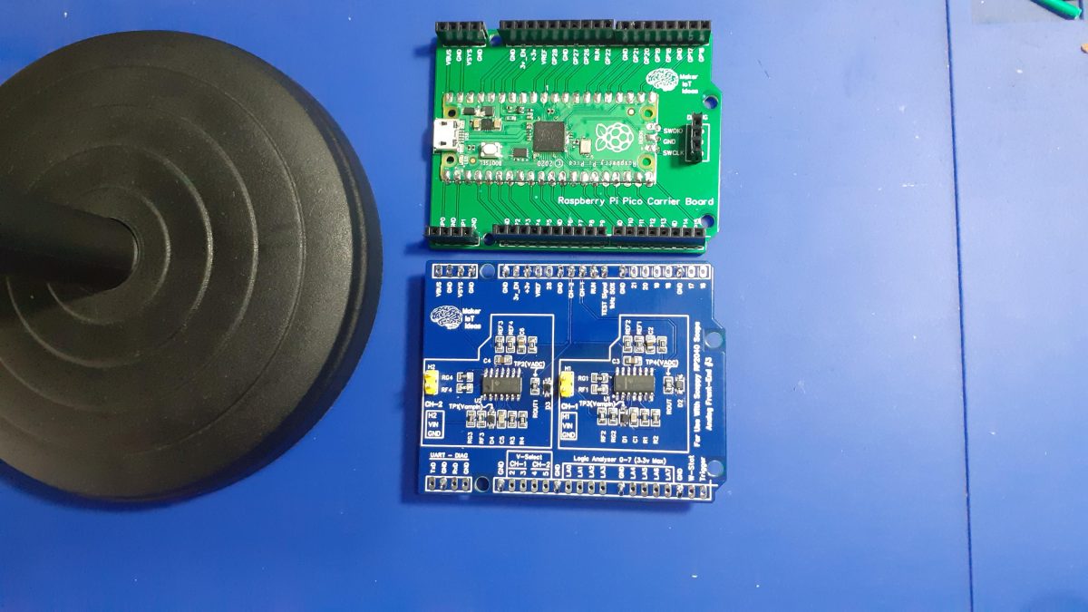
The PCB is a dual-layer shield that is designed to be used with the MakerIOT2020 Raspberry Pi Pico Carrier board. The shield is directly powered by the carrier board.
The original Analog Front-End #3 circuit featured a single channel input, capable of accepting a -18.0v to 18.0v signal input.
My changes were limited to doubling up on that circuit, to provide two channels.
I have redrawn the original schematic, partly to make it easier to understand for myself, as well as to help me with the design of the PCB.
Lets take a look at the schematic ( by using text from the original designer) The author makes no warranty, representation or guarantees regarding the suitability of this design for any particular purpose. Nor does the author assume any liability arising out its use and specifically disclaims any and all liability, including without limitation special, consequential or incidental damages.
This design builds on Design 2 and adds over and under voltage protection to the analog front end. After all, we won’t have a cheap oscilloscope if we keep frying our components!
I’m assuming here that the minimum and maximum voltages that will be applied to the input of the scope will be -18V and +18V respectively. It has been tested from -18.5V to 18.5V (two of my 9V batteries in series) but of course If you decide to use this design you are doing so at your own risk. I personally wouldn’t use Scoppy with an expensive phone/tablet just in case something unexpected goes wrong (better to use an old, obsolete phone that is no longer used for anything else) – especially when dealing with higher voltages – but of course you can do what you like.
Protecting the Op-Amp input(s)
First of all we need to protect the op-amp. In this design we’ll be using an LM324 op-amp, which is very similar to the LM358 but contains four individual op-amps rather than two. We’ll be using three of these op-amps. The reason for this will be explained later.
According to the datasheet for the LM324 the allowed input voltage range goes from -0.3V to 32V. Of course 32V is above the maximum expected voltage (18V) and so we don’t need to worry about over-voltage protection. However we do need to ensure that the voltage at the input pins don’t go below -0.3V. A schottky diode can be used to clamp the voltage to something above -0.3V (D1 in the schematic).
One thing that needs to be considered when selecting the diode is its reverse current. The 1N5817 has a very low forward voltage but high reverse current and this results in a voltage drop at the input of the op-amp (in the order of 100mV). Presumably this is because it draws current through the high value input resistor (Rg1). The 1N5711 has a much lower reverse current specification and I couldn’t discern any voltage drop when this was inserted into the circuit. However, its forward voltage (at the current expected in this part of the circuit) is very close to the minimum allowed voltage of -0.3V. To be safer I prefer to use something like a BAT46. It does result in a voltage drop of a few millivolts but the clamped voltage is more like -0.23V.
Protecting the Pico/RP2040
The Pico datasheet states that:
the ADC capable GPIO26-29 have an internal reverse diode to the VDDIO (3V3) rail and so the input voltage must not exceed VDDIO plus about 300mV
The obvious way to protect the ADC inputs (GPIO26-29) then is to simply insert a schottky diode between the ADC input and VDDIO. However, the RP2040 datasheet says that:
the voltage on the ADC analogue inputs must not exceed IOVDD ...<snip>... Voltages greater than IOVDD will result in leakage currents through the ESD protection diodes
That suggests to me that we shouldn’t be allowing current to pass (leak) through our clamping diode and into IOVDD. I could be completely wrong here – if you think so then please share your thoughts in the forum (Discussions).
Anyway, to be safe we’re going to avoid that situation by sending the current to the output of one of our op-amps (LM324-sink on the schematic). The LM324 is able to sink up to ~10mA so this should work fine if we limit the current from the main op-amp (LM324-amp in the schematic). Given that the maximum voltage expected at the output of LM324-amp is around 4.5V (Vcc – 1V) then we need a resistor of at least 120R to limit the current to 10mA (4.5-3.3 / 0.010 = 120). A 220R resistor should do fine (Rout).
And of course the reason we are using an LM324 rather than the LM358 of the previous designs is that three op-amps are required.
A 1N5817 diode (D2) is used here (rather than a BAT46 – used on the input of LM354-amp) because at the expected maximum current of 10mA the forward voltage drop of the BAT46 is higher than 300mV. The high reverse current of the 1N5817 is not such an issue here because Rout has a low value and so there will only be a small voltage drop across Rout when D2 is reverse biased.
Construction
Here are some instructions for assembling this front end on a breadboard. The pin numbers refer to the LM324 PDIP package. Refer to the schematic and breadboard image above. NB. The rail labelled 5V on the schematic is actually VSYS which of course is not necessarily 5V because it depends on how charged the battery is on your Android device.
Connect 3V3 of the Pico to the top red power rail of the breadboard. Connect VSYS to the bottom red power rail. Connect both ground rails of the breadboard to one of the GND pins of the Pico. The fuse as shown in the breadboard image is optional.
Connect the Vcc pin of the LM324 to the VSYS rail. Connect the GND pin of the LM324 to the GND rail. Don’t connect anything to the ADC pin(s) of the Pico yet.
Now we’ll configure each of the 4 op-amps of the LM324 in turn.
The voltage at the non-inverting input should be approximately VSYS/2 and the output should be the same.
Op-amp 4 – Vref Wire up this op-amp as shown in the schematic. The voltage at the output should be approximately 1.65V.
Op-amp 3 – sink Wire up this op-amp as shown in the schematic. The voltage at the output should be 3.3V.
Op-amp 1 – amp Wire up this op-amp as shown in the schematic, including the under-voltage protection diode on the input (D1) and the current limiting resistor (Rout) and over-voltage protection diode (D2) on the output. Don’t connect the output to the Pico yet.
Testing and initial operation
You should now be able to safely apply any voltage at Vin1/Vin2 of between -18V and +18V. Test that the voltage at the input of the LM324 (Vampin) doesn’t go below -.3V and the voltage at the output of op-amp 2 after Rout (Vadc) doesn’t go above 3.6V.
Once you’ve confirmed that all of the op-amps have been wired correctly you can connect the output of Rout to the ADC pin of the Pico.
The author makes no warranty, representation or guarantees regarding the suitability of this design for any particular purpose. Nor does the author assume any liability arising out its use and specifically disclaims any and all liability, including without limitation special, consequential or incidental damages.
Designing the PCB
PCB Design and Layout
Manufacturing the PCB
The PCB for this project has been manufactured at PCBWay. Please consider supporting them if you would like your own copy of this PCB, or if you have any PCB of your own that you need to have manufactured.
Assembly
The PCB was assembled with help of a stencil to ease and speed up the solder paste application. The components were then hot-air soldered. As this is only a prototype, I chose to only place 2.54mm header pins on pins that are required for operation, as well as all the ground pins, to ensure a proper ground plane.
SMD Stencil to speed up assemblyAfter AssemblyAFE with Raspberry Pi Pico Carrier boardTop viewStacked, side viewStacked, top front viewStackedBack view
Conclusion
This was quite an interesting project. While everything works as expected, resolution and frequency are limited. ( of course, it is…) The project is however still useful, and will definitely give you some useful results in a pinch.
The logic analyser is by far more useful, but once again, a commercial device will be way more accurate and useful for professional use. Hopefully, the designer will add some protocol filters etc in future.
This device will not replace a proper oscilloscope or logic analyser, but it will definitely give enough accuracy and resolution on low-frequency applications to satisfy some of the basic needs of a beginner or student just starting out with electronics.
It is also important to note that you should be safe, and not try to connect this to high voltages etc. Also, don’t connect this to your expensive phone or tablet, use an old one instead, as accidents may happen, and we don’t want to damage our valuable handheld devices…
In Part one, we took a very quick look at the installation of the firmware, as well as the basic limitations for use of this very useful project.
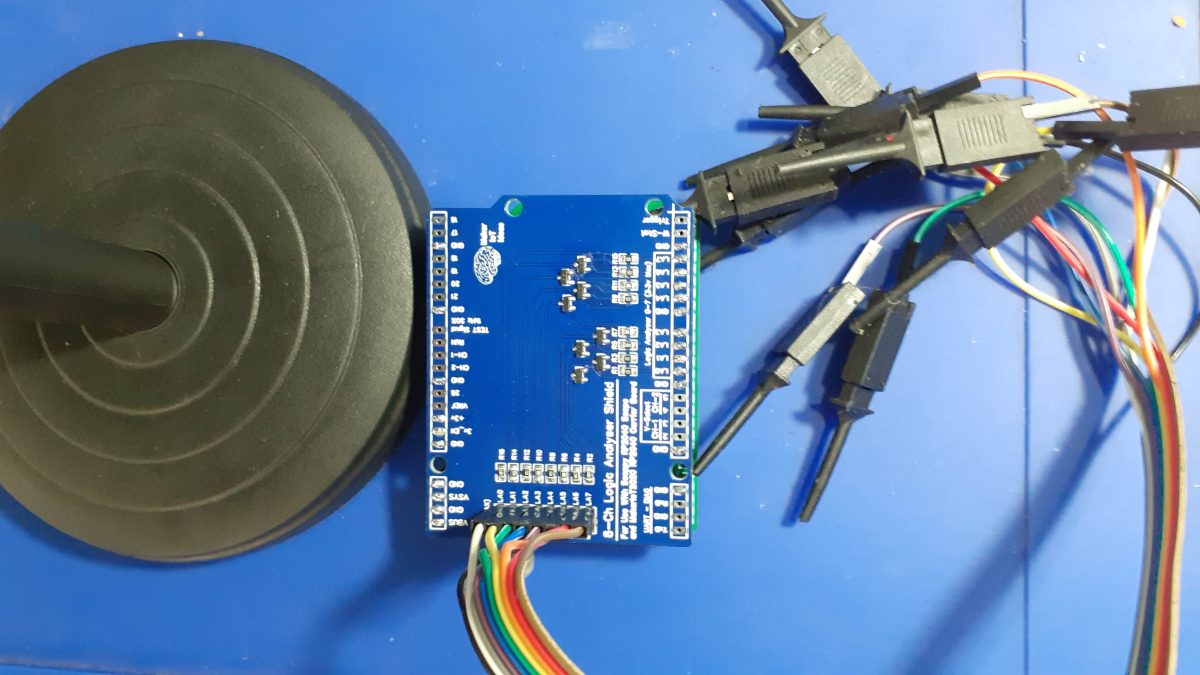
In this part, I want to take a quick look at my Logic Analyser shield, for use with this project, as well as the Raspberry Pi Pico Carrier Board. In part one, we saw that the logic analyzer inputs are limited to 3.3v by the RP2040 GPIO pins. This shield is a prototype attempt to overcome those limitations by using logic-level conversion.
8 Ch Logic analyser Shield for use with Scoppy and MakerIOT2020 Pico Carrier Board
All Raspberry Pi Pico pins are broken out and labelled, as well as all of the pins specific to the Scoppy App have been clearly labelled. The board are stackable onto the Pico Carrier board, via standard 2.54mm Male Headers, or extra long, stackable female 2.45mm headers, similar to those found on common Arduino shields.
The use of stackable headers will allow simultaneous use of the logic analyser shield and the Analog frontend shield, introduced in part 3 of this series.
In addition to that, a 2×8-way 2.54mm Male header provides access to the 8 logic converted logic analyser inputs.
Logic conversion is done with a simple circuit, comprising a Bss138 N-Channel Mosfet and two 10K resistors per channel.
The shield is powered directly from the Pico Carrier board, which is in turn powered from the OTG cable to the Android Phone or tablet used to display the captured data. ( see Part 1 for installation instructions and other details regarding the Scoppy Project)
The logic level converters allow the use of a 5v logic signal, which is an improvement over the original design, which allowed only 3.3v inputs.
The PCB for this project has been manufactured at PCBWay. Please consider supporting them if you would like your own copy of this PCB, or if you have any PCB of your own that you need to have manufactured.
Some more pictures of the device
FrontBackAssembled FrontAssembled BackLogic analyser shield together with RP2040 carrier boardStacked view 1Stacked view 2Stacked with logic probes
All credits for the development of the Scoppy firmware goes to fhdm-dev. This shield is a modification made by MakerIOT2020, and thus belongs to me. In the spirit of the original project, It will however be released to the public as a free open-source project ( free as in free download, free schematic, free design ). The PCB manufacturing files will be made available for free at a later stage, or can be ordered from PCBWay from this link
Oscilloscopes and Logic analysers are essential instruments for every serious electronics hobbyist. They are however quite expensive, and thus beyond the reach of many people starting out with electronics. Today, I will show you a cheap solution, an RP2040 Oscilloscope and Logic analyser…
Before we get started, we need to clear up a few things first: 1). This is not my own project. It was designed and built by someone else. 2). This is not a professional grade Oscilloscope or Logic analyser 3). The range of input voltages, as well as the frequencies that you can measure, are limited.
What is this, and why do I bother with it?
This post is about the Scoppy Occiloscope Firmware, designed by fhdm-dev. I have no affiliation with him/her, I came across this recently and found it useful in the sense that it may help others gain access to instrumentation to greatly help them with electronics.
I did design some derived pcb components that works with this project, in order to take care of some limitations that I saw in the original project. More on that in two follow-up posts, in which I will show you two PCB’s that I designed to use with this project, and analog Frontend ( based on a public design by fhdm-dev, as well as a Logic analyser shield, of my own design
before we do this, we need to look at the basic Scoppy design and its firmware.
Getting Started
You will need a few things to make use of this project, the most important will be the Scoppy App ( available from the Google Playstore ), and an Android Phone. You will also need a USB OTG Cable/hub for the phone, as well as a Raspberry Pi Pico or Pico W
I have decided to use my own Raspberry Pi Pico Carrier board for this project, as it will allow me to get away from the breadboard, as well as serve as a platform for easily expanding on the project via expansion shields, as you will see in later articles.
Makeriot2020 Raspberry Pi Pico Carrier Board
This PCB, in Arduino Uno form Factor, will make putting the entire project into a case quite easy, as well as hopefully keep the number of floating hookup wires to a minimum. ( hopefully reducing some notice and other stray signals from interfering too much with our signals)
After installing the application, which is quite easy, we need to load the firmware onto the RP2040. This is also extremely easy is you follow the guide at the top.
Please note that the Android app has two modes, a freeware mode, limited to one channel, and a paid version, with no limitations. I recommend that you consider buying the paid version, as it only costs a few dollars ( I paid $USD2), and will motivate the developer to keep working on the project, and improving it.
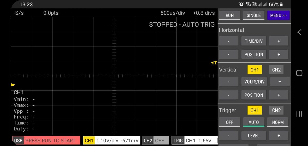
Scoppy Application, Main Interface – OscilloscopeScoppy MenuScoppy Logic Analyser Screen
As we can see, the interface is quite clean, and easy to use.
What are the limitations?
There are quite a few limitations, namely frequency and voltage input. From what I can understand, the frequency limit seems to be around 25Khz, with the voltage level limit being 0.0v to 3.3v ( as per the limit of the RP2040 ADC
Please make sure that you follow all instructions on the original page, as you can very easily damage your Android device as well as the Pico if you apply a voltage outside of the allowed range.
On the logic analyser side, It is also important to note that you should stay in the 0.0v to 3.3v range of the Pico GPIO’s.
While these limited ranges will definitely limit what you can do and measure, It will still be a very useful project. In the next part of this article, I will show you how I have solved the logic analyser voltage range issue… Allowing you to analyse 5v signals as well.
In this post, we will look at a versatile easy-to-use XIAO RP2040 LoRa Fusion. The SEEED Studio Xiao RP2040 should, by now, no longer be a stranger to any of us makers and electronics enthusiasts. At its heart, it contains the same RP2040 processor that is used on the Raspberry Pi Pico.
What makes, the Xiao RP2040, special is its size, only 20.00mm x 17.5mm, as well as the carefully curated combination of GPIO pins, single-sided board construction and castellated pads to make incorporating it directly into a design an absolute pleasure.
Features
Powerful MCU: Dual-core ARM Cortex M0+ processor, flexible clock running up to 133 MHz
Rich on-chip resources: 264KB of SRAM, and 2MB of onboard Flash memory
Flexible compatibility: Support Micropython/Arduino/CircuitPython
Easy project operation: Breadboard-friendly & SMD design, no components on the back
Small size: As small as a thumb(20×17.5mm) for wearable devices and small projects.
Multiple interfaces: 11 digital pins, 4 analog pins, 11 PWM Pins,1 I2C interface, 1 UART interface, 1 SPI interface and 1 SWD Bonding pad interface.
Specifications
Item
Value
CPU
Dual-core ARM Cortex M0+ processor up to 133MHz
Flash Memory
2MB
SRAM
264KB
Digital I/O Pins
11
Analog I/O Pins
4
PWM Pins
11
I2C interface
1
SPI interface
1
UART interface
1
Power supply and downloading interface
Type-C
Power
3.3V/5V DC
Dimensions
20×17.5×3.5mm
The AI-Thinker RA-02 also need no introduction from me, as I have used it extensively in quite a few projects before.
With the worldwide chip shortage, building solutions around the easily available RP2040, and RA-02 makes perfect sense, as these two modules are also super cheap.
For this project, I have also decided to try out a fully factory-assembled PCB to compare quality, as well as the convenience of being able to focus on software without doing assembly first, not that I mind assembling my own boards though… More on that experience later…
What were my intentions with this project?
I had the following goals/needs: 1. A modern, easily obtainable processor, that is not only cheap but also energy efficient. The RP2040, in the form of the Xiao RP2040, fits that goal perfectly. 2. An as-small-as-possible footprint for the main processor, without having to resort to manually designing a Pi Pico derivative – The RP2040 chip is a bit tiny for my eyes 3. The minimum of external supporting components to make the design function 4. Flexible power options ( 3v or 5v )
As to my use intentions, I use quite a few LoRa devices for various different purposes, so adding another option seemed like a good idea.
In the current design, providing that the Arduino libraries stay compatible, the new design will support not only LoRa but also FSK and OOK, with all the advantages of those.
By changing the position of only 3 jumpers, I can also use the PCB for a general-use RP2040 development platform, or another RP2040 project.
Taking all of this into consideration, the device will thus be ideal for any remote sensor application, as well as using it on the bench-top for prototyping
What features are on the PCB?
All of the Xiao RP2040’s pins and pads are broken out onto the PCB, including the SWD port.
The Xiao also has a user LED, and a NeoPixel on-board, which can easily be used for signal indication.
Level shifted 5v I2C port, in addition to the standard 3.3v I2C, because all of our sensors are not always 3.3v compatible, and using external level shifters is not always so convenient.
Access to the RA-02’s GPIOs (DIO1-DIO5) is provided, but most people won’t need to worry about these.
Jumpers to connect some of the Xiao RP2040 GPIO to the special use GPIO on the RA-02, for example, GPIO1 and GPIO2, sometimes used with some of the more specialised LoRa libraries.
Provision or powering the device via a dc barrel connector, or screw-terminal, as well as via the 3v input pins (make sure your supply has a capability of more than 300mA)
A power management chip to reset the Xiao RP2040 when the supply voltage falls below 3.0v – To prevent unstable operation and possible lock-up.
For this project, I have decided to try out SEEED STUDIO’s Fusion Service. They are after all the manufacturers of the Xiao RP2040 Module that I used, so, when they contacted me a few weeks ago with an invite to try out their Fusion service, I decided to give it a go.
Seeed Fusion offers one-stop prototyping for PCB manufacture and PCB assembly services, and as a result, they produce superior quality PCBs and Fast Turnkey PCBA in as little as 7 working days. When you prototype with Seeed Fusion, they can definitely provide Free DFA and Free functional tests for you!
So, what was my experience like?
From a design point-of-view, nothing much changed, except that I had to spend a bit more time focusing on the BOM, as my usual go-to for components is LCSC. I, therefore, had to make a few small substitutions on some passive components to ensure that everything was in stock and available.
I also chose to only have the SMD components on the PCB factory assembled. Soldering a few header pins is no trouble anyway.
Manufacturing and shipping lead times were not too long, and I received the assembled boards in about 7 working days from the time of order.
Using the PCB
The Xiao RP2040 has great support for Micropython, CircuitPython as well as the Arduino IDE. There is an excellent article on getting started with the XIAO RP2040 available here , with sections on all three supported development languages and environments.
You can also try out some machine-learning projects with TinyML
As mentioned above, most of the 11 GPIO pins on the XIAO RP2040 were broken out to headers on the PCB, with the exception of those needed for dedicated control of the RA-02 LoRa Module ( D1, D2, D8, D9, D10). In addition to this, some other GPIO, like the I2C pins (D4 and D5) may be accessed on H1 (labelled as SCL/SDA) [3.3v logic] or alternatively on H2 (as SCL/SDA) [ note that this header is level converted to 5.0v ]
To accommodate some other special use features of the RA-02 LoRa Module, J1 and J2 can be jumpered in two positions to connect D3 to DIO1 on the RA-02, and D6 to DIO2 alternatively. Most people will however not need to do this.
When using the Hardware UART on the Xiao RP2040, the jumper at H4 needs to be set to D7/Rx->D7 in order to receive Data, and J2 should be in the default D6/Tx->D6 position
PCB Layout – Showing Jumpers and Headers
Testing the PCB with LoRa
In order to test the functionality, I have written a very simple sketch to test the communication between the PCB and another LoRa device, running a similar sketch…
#include <SPI.h>       // include libraries

#include <LoRa.h> // I used Sandeep Mistry’s LoRa Library, as it is easy to //use and understand


const int csPin = D7;     // LoRa radio chip select

const int resetPin = D1;    // LoRa radio reset

const int irqPin = D2;     // change for your board; must be a hardware //interrupt pin

byte msgCount = 0;      // count of outgoing messages

int interval = 2000;     // interval between sends

long lastSendTime = 0;    // time of last packet send

void setup() {
Serial.begin(115200); // initialize serial
while (!Serial);
Serial.println("LoRa Duplex - Set spreading factor");
// override the default CS, reset, and IRQ pins (optional)
LoRa.setPins(csPin, resetPin, irqPin); // set CS, reset, IRQ pin
if (!LoRa.begin(433E6)) { // initialize ratio at 433 MHz
Serial.println("LoRa init failed. Check your connections.");
while (true); // if failed, do nothing
}
LoRa.setSpreadingFactor(8); // ranges from 6-12,default 7 see API docs
Serial.println("LoRa init succeeded.");
}
void loop() {
if (millis() - lastSendTime > interval) {
String message = "Testing Xiao RP2040 - LoRa "; // send a message
message += msgCount;
sendMessage(message);
Serial.println("Sending " + message);
lastSendTime = millis(); // timestamp the message
interval = random(2000) + 1000; // 2-3 seconds
//msgCount++;
}
// parse for a packet, and call onReceive with the result:
onReceive(LoRa.parsePacket());
}
void sendMessage(String outgoing) {
LoRa.beginPacket(); // start packet
LoRa.print(outgoing); // add payload
LoRa.endPacket(); // finish packet and send it
msgCount++; // increment message ID
}
void onReceive(int packetSize) {
if (packetSize == 0) return; // if there's no packet, return
// read packet header bytes:
String incoming = "";
while (LoRa.available()) {
incoming += (char)LoRa.read();
}
Serial.println("Message: " + incoming);
Serial.println("RSSI: " + String(LoRa.packetRssi()));
Serial.println("Snr: " + String(LoRa.packetSnr()));
Serial.println();
}
Please note that the sketch uses callbacks on receiving messages.
In conclusion
This project was quite interesting, and I am very much impressed with the quality of the assembly done by SEEED Studio’s Fusion Service. The Xiao RP2040 is also a pleasure to work with, and I hope that with future iterations of this prototype, I may be able to produce an even more compact PCB, that will still pack some serious performance punches while being power efficient as well
While my recent ESP32-S Dev Board really does the trick to help my development cycle along, I very quickly ran into another obstacle, in the sense that, after doing stuff on the breadboard, moving those components onto a more permanent location, either as a next stage prototype or more likely that the project is so small and insignificant not to warrant the effort actually to design a PCB for it. This could be rectified by using another one of my recent designs, an SMD breadboard PCB, but that would not always do either.
MakerIoT SMD Prototype development PCB
That got me thinking, and while staring at the ever-present Arduino Uno on its corner of the work-bench, I suddenly remembered that I have once seen an Arduino Prototype Shield, like a plug-on breadboard, with breakouts of all the pins etc…
While I do not personally own a lot of commercial Arduino Shields, as I tend to build my own or design a custom-purpose PCB instead, it did not take me long to settle on a new design, that could potentially solve my problem, and hopefully, someone else’s as well…
So what is on this PCB?
To start off, the PCB is in the same form factor as the ESP32-S Dev Board, namely the Arduino Uno form factor. There are however a few changes, mainly in the number of pins in the headers. This is mainly to accommodate as many of the ESP32-S’s gpio’s as possible. ( Actually, they are all broken out, EXCEPT for the 6 gpio’s that are usually used with the internal Flash memory.)
The PCB is designed to be stacked either on top of, or even below, the ESP32-S Dev Board, depending of course on the type of headers that you decide to solder onto the PCB.
In order to make connecting to the gpio pins easier, each header row is in fact a double row, with solderable pads in parallel for each gpio on the header row.
Flash and Reset buttons are available on top of the shield, they can be fitted of left off, depending on personal preference, as well as how the shield will ultimately be used.
The prototyping area in the centre has been slightly reduced from the standard 5-pin-spacer-5-pin column of the traditional breadboard to a 3-pin-gnd-3v-3-pin column layout. the prototyping holes are at a standard 0.1″ or 2.54mm pitch.
In total, 60 prototype holes, divided into rows of 10, 3 columns deep, are provided, labelled A-F and 1-10.
3.3v and ground are provided in the centre-two rows, to make power easily accessible.
ESP32-S DEV Prototype ShieldESP32-S Dev Prototype Shield – Back
The PCB Design
As this design is basically just two rows of header pins, with a few switches, and a big unconnected prototype area, I did not bother to do a formal schematic for this PCB, but instead jumped straight into the PCB design software and manually designed and routed the tracks and pads that make up this shield.
PCB – Top Layer PCB – Bottom Layer – Note that this is a “TOP-Down” view, and should be mirrored for actual production
Note that there are big copper pours on both top and bottom layers, in an attemp to reduce electrical noise and provide better shielding.
Manufacturing
The PCB for this project has been manufactured at PCBWay. Please consider supporting them if you would like your own copy of this PCB, or if you have any PCB of your own that you need to have manufactured.
Top viewTop view – Not assembledBottom view – AssembledBottom view – Not assembledSide-by sideSide by SideStacked – Side viewStackedStacked – top viewStacked – from front
Conclusion
Some final thoughts on the completed PCB. While definitely useful, I have made a purpuseful design flaw on this board, by not including a breakout for the VIN pin. My reasoning at that stage was that I would always be powering the device directly from 3.3v, and would therefor not need access to the VIN pin for power.
Upon completion of the device, and while testing it in a stacked configuration, I realised that that VIN pin would have been quite nice to have access to.
Not a big problem though, as if is very easy to add a 2-pin connector to the power rails, or even solder a wire directly to VIN. Ugly, but totally doable, as this is in fact still a prototype, and it can grow and be fine-tuned to my exact requirements over time.
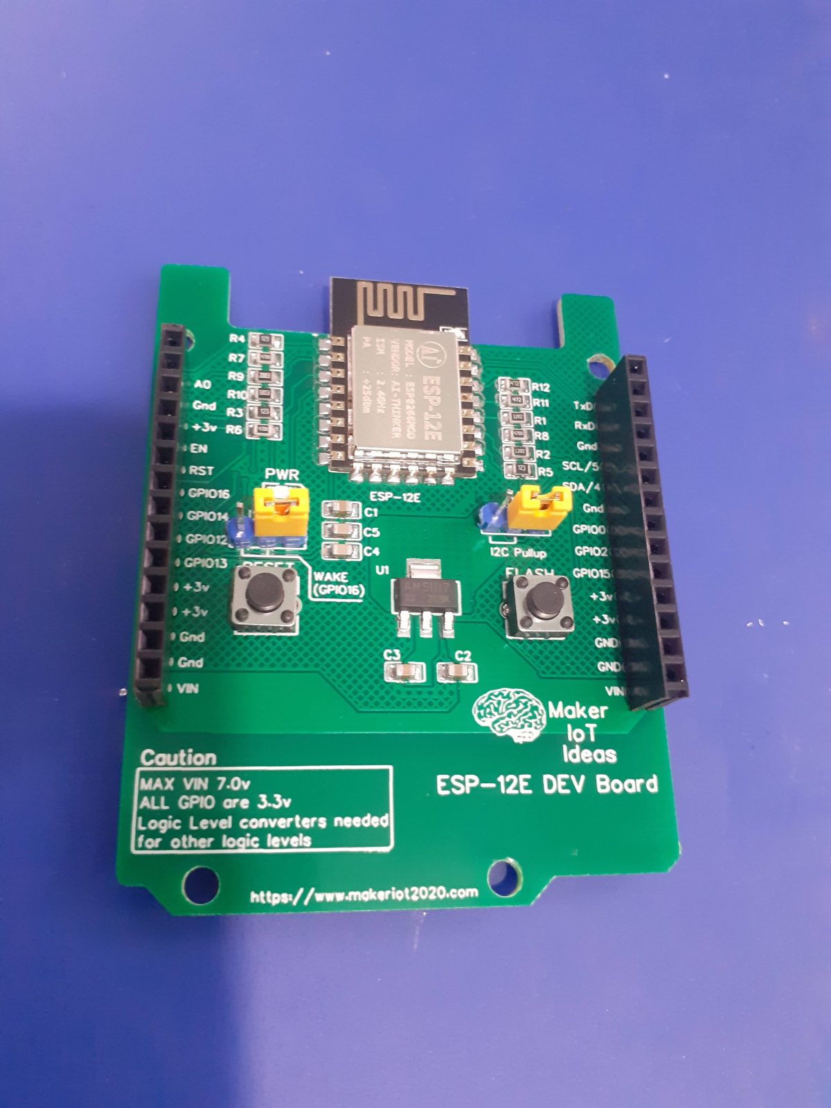
As a followup to my recent ESP32-S in Arduino Form Factor device, I decided to also produce a similar circuit board for the ESP8266-12E. Although some people mostly consider these as obsolete, I still find them extremely useful for small projects, and thus use quite a lot of them.
With their lower total pin count and similar low cost to the bigger ESP32 modules, these do force you to get quite creative with the available pins, as well as how and what you can interface.
ESP8266-12E in Arduino Form Factor, with optional I2C pullups as well as Wake from sleep function on GPIO16
What is on the PCB?
For this design, I have once again tried to keep it very lean, including the absolute bare minimum supporting components needed for correct operation. This includes pull-up and pull-down resistors on the various strapping pins, as well as some decoupling capacitors.
I also did not include a USB-to-Serial converter circuit, as these are used only once or twice, and also consume power while not being needed all the time. As most of my devices are uploaded OTA anyway, an external stand-alone USB-to-Serial adapter is perfect to upload the initial firmware.
Jumpers to control the onboard I2C pullup-resistors, as well as the Wake-up-from-deep-sleep function on GPIO16 were also added, in addition to the Reset and Flash push-buttons to place the device into initial programming mode.
A 3.3v LDO regulator was also added, for convenience mostly, when powering the device from a bench power supply unit. The recommended voltage for this LDO would in my opinion be 7v Dc, although the datasheet states it can be up to 15v DC… In my opinion, that stresses the component a bit much though, as most of that excessive voltage is dissipated as heat.
PCB Layout – Blank board, front and back
Blank ESP-12E Dev board PCB – FrontESP-12E Dev board- Back
To try and minimise heat-related issues with the LDO regulator, I have incorporated an on-PCB heatsink for the LDO regulator, which is via-stiched together on both sides of the PCB. This type of heatsink seems to work quite well in many of my other designs, so I decided to use it here as well.
I have also made use of big copper pours on both sides of the PCB to ensure that there is a good ground plane, as well as make use of differential pairs for the routing of the UART and I2C tracks.
Schematic
ESP-12E Dev Board Schematic
PCB Design
Manufacturing
The PCB for this project has been manufactured at PCBWay. Please consider supporting them if you would like your own copy of this PCB, or if you have any PCB of your own that you need to have manufactured.
PCB fresh out of the PacakageBack side of final assemblyFinal Assembly – frontAfter reflowing the SMD componentsBefore Reflow of SMD ComponentsSMD Stencil to make life a bit easierAfter Solderpaste application
Procedure to upload initial firmware
Due to the fact that this device does not have an onboard USB-to-UART (Serial) converter, it will be necessary to use an external device the first time that you upload firmware, or while you are using it on the bench if you do not want to use OTA…
The easiest way to do this, in my opinion, is the following: 1) Power the device from a bench power supply, set at 7V DC via the VIN and GND Pins, available on the bottom left and right of the device ( you can use either side, not both 🙂
2) Now connect your external USB-to-UART converter to the device, as follows: UART Converter <-> ESP-12E Dev Board Rx <- TxD Tx -> RxD Gnd — GnD
Do Not connect the power (VCC) from the USB-to-UART Converter!
Now start your Adruino IDE, or similar, and connect to the Serial monitor. Press the reset button on the board, and watch for output in the serial monitor.
If you see output, at 115200 BPS, press end hold flash, and then press and let go of reset, while still holding the flash button.
Wait a few seconds, and then upload your sketch, remembering to manually reset the board after the upload has completed.
I would recommend that you upload the Arduino OTA sketch, from the examples, and modify it to connect to your local WiFi. That way, you will be able to upload all following sketches via your local Wifi, providing that you do not remove the OTA code from the sketch.
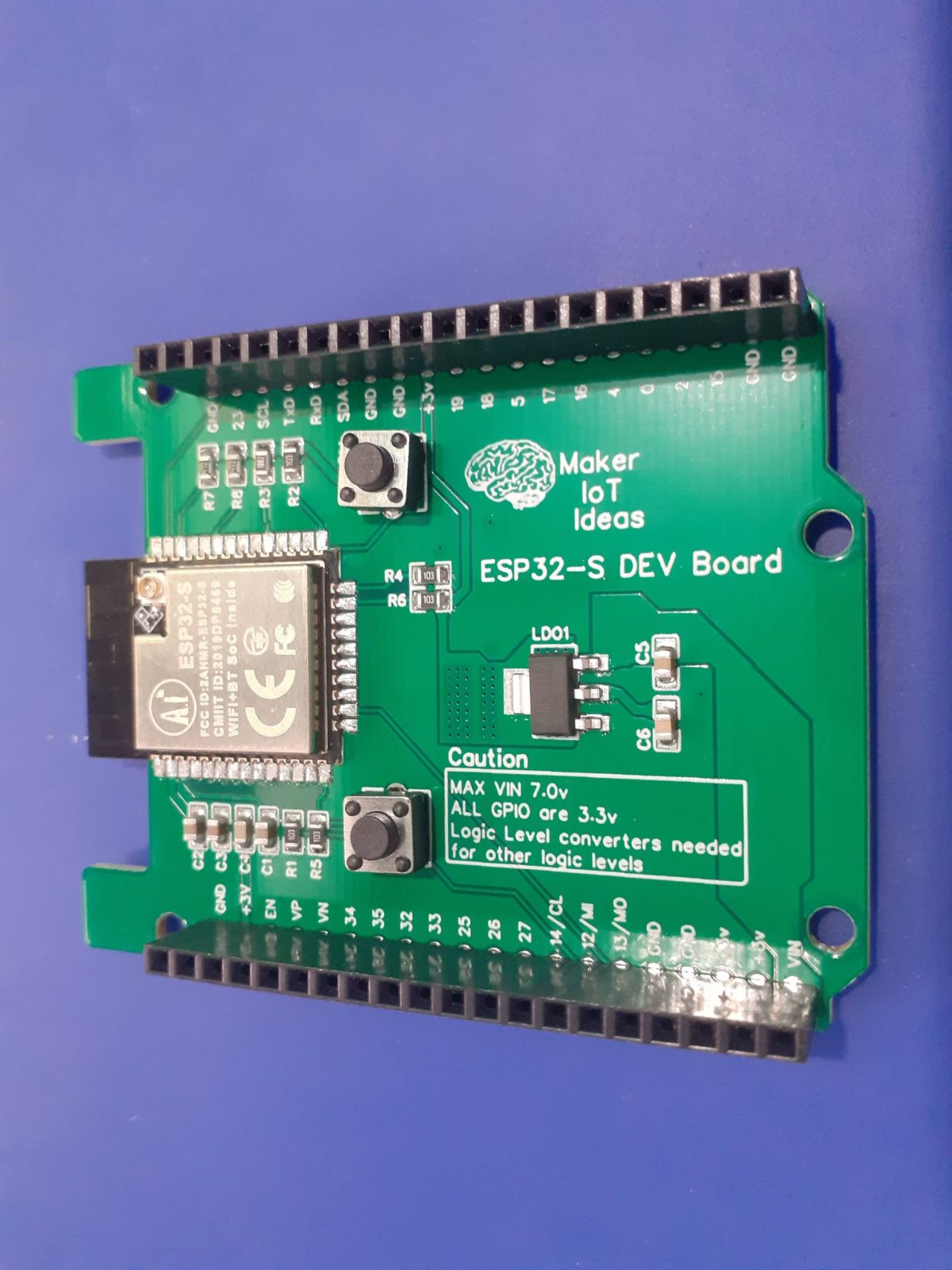
The ESP32-S is, at least in my opinion, one of the most versatile microcontrollers available to the Maker at this moment. It ticks almost all of my boxes for features required in a microcontroller, with a lot of gpio’s, WiFi, and Bluetooth, as well as a lot of storage space for code.
I do however have an issue with it, which I usually get around by designing a custom circuit board with a specific purpose. This is great for a project, but as most projects do not start on a custom-built circuit board, I am usually required to use a breadboard module. This is where my problems start. These modules are cumbersome to fit on a breadboard, to say the least, taking up a lot of space, and leaving very little space to connect to its pins with anything else.
Some of these modules do not even fit on the breadboard, making it necessary to hang one side off the breadboard or use two breadboards with a gap in the middle. I am quite sure many people can relate to this problem.
My second issue is that when you have done your breadboarding, and want to go to a permanent project, which does not always need a dedicated PCB, you are now required to either live with things on a breadboard, scary to say the least or have a “spider” with many modules and wires, in a box or partly on protoboard etc…
My Solution, the ESP32-S DEV Board, in Arduino Uno form factor
While not the most elegant, personally I really like the size, and layout of the humble Arduino Uno, with its standardised pinouts, and a large number of addon shields available for the platform. This made me think, sure, there are already ESP32-based boards in this form factor available commercially, but why not make my own instead, as well as a few of my most used modules in a standardised shield form, to make my life just that little bit easier?
The picture above shows my attempt, with most of the GPIO broken out onto female header pins (except for the 6 gpio that are connected to the internal flash chip on the module).
The Blank PCB ( front )PCB- Back
The PCB explained…
Power: The board can be powered in two ways, either via the VIN pin ( at an optimal 7.0v DC – the LDO regulator can handle up to 15v, but I personally find that to stress it a bit hard ), which will use the onboard LDO voltage regulator to provide the needed 3.3v or from an external 3.3v PSU, which can provide a bit more current if needed…
There are also plenty of 3.3v and ground connections on the two 20-way headers to connect to other sensors.
Strapping Pins All the required strapping pins are pulled up or pulled down, as per the datasheet, to 3.3v or ground respectively.
GPIO Pins All GPIO pins are clearly labelled on the silkscreen to make it easier to use. I did however not stick to the Arduino labelling convention, as I don’t always use the Arduino IDE, and the actual GPIO numbers are in my view, more useful then.
Flashing code to the board
It will be quite obvious that I did not include any USB-to-serial converter on the board, the reason for this being that, in my opinion, 1) it wastes space on the board 2) it is not actually necessary, as we can upload with an external uart adapter, or use OTA ( which I actually do most of the time ) 3) In an actual project, that USB port is going to attract problems, especially if you give it to someone else to use…
A simple Arduino OTA sketch is available in the examples section of the Arduino IDE. It is easy to use and modify and does not need a lot to make it useable with your own sketch…
Antenna Cutout
As recommended by the manufacturer , I have chosen to place the chip inside a cutout on the top of the PCB, with no tracks nearby.
Figure 17: Keepout Zone for ESP32 Module’s Antenna on the Base Board
Although this is not the ideal “best position”, I found that this position worked well with previous designs, and have thus kept it at that.
General comments
As this board is mainly designed for prototype development, I did not bother with dedicated power connectors etc. I did however add proper wide tracks for all the power connections, an on-PCB-heatsink for the voltage regulator, as well as proper ground planes on both sides of the PCB, connected together with via-stitching where needed.
It is also very important to note that this is a 3.3v device. If you need to use sensors or peripherals that operate at other voltages, you will have to use external level converters.
Some assembly pictures
After Solderpaste applicationBefore ReflowAfter ReflowAfter final assembly
Schematic
Manufacturing
The PCB for this project has been manufactured at PCBWay. Please consider supporting them if you would like your own copy of this PCB, or if you have any PCB of your own that you need to have manufactured.


