
The ATTiny1616 is a step up from the ATTiny202, having more GPIO, flash and RAM. This makes it ideal for bigger, but still medium size projects that do not need all the power of the traditional Arduino.
In Part 1 of this series, I took a quick look at the ATTiny202 MCU from Microchip. Having only 5 useable GPIO, with limited Flash and Ram, that little chip was still quite useful for some of those very small projects, where we did not really need a lot of peripherals and GPIO pins.
Today, we shall take a step up, and take look at a slightly bigger MCU, the ATTiny1616, this time with up to 17 GPIO pins, more flash and memory, and still quite easy and cheap to get hold of. (Current Prices are in the range of about $1USD to $2USD, depending on where you buy and how many you buy).
As I wanted to give myself a bit of a challenge with this project, I decided on using a QFN package this time, which, being extremely tiny, only 3mmx3mm, will give most Makers a pleasant challenge to solder correctly. ( I am planning a SOIC 20 version, but with a bit more external hardware onboard)
The ATTiny 1616 is part of the tinyAVR-1 series, which includes the 1614,1616, and 1617, and they have the following features ( copied from the datasheet link above)
The ATtiny1614/1616/1617 are members of the tinyAVR® 1-series of microcontrollers, using the AVR® processor with hardware multiplier, running at up to 20 MHz, with 16 KB Flash, 2 KB of SRAM, and 256 bytes of EEPROM in a 14-,20- and 24-pin package. The tinyAVR® 1-series uses the latest technologies with a flexible, low-power architecture, including Event System, accurate analog features, and Core Independent Peripherals (CIPs). Capacitive touch interfaces with Driven Shield+ and Boost Mode technologies are supported with the integrated Peripheral Touch Controller (PTC).
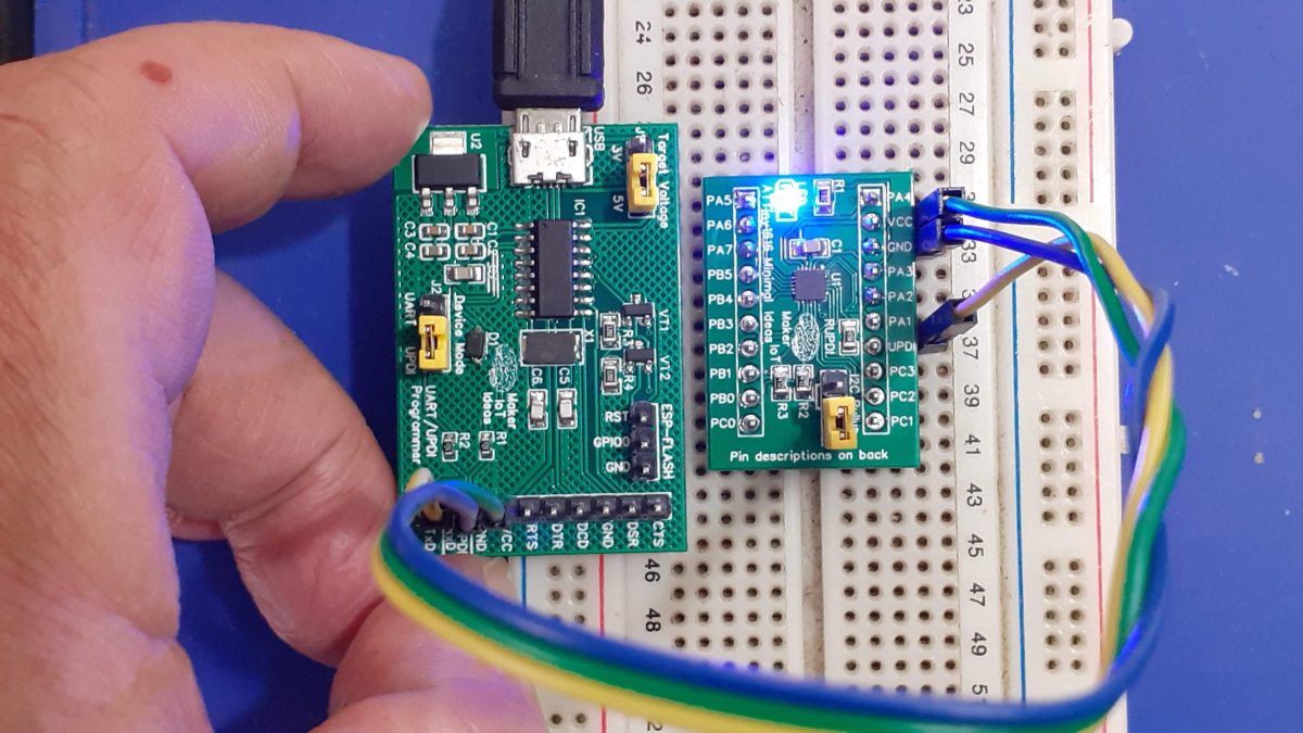
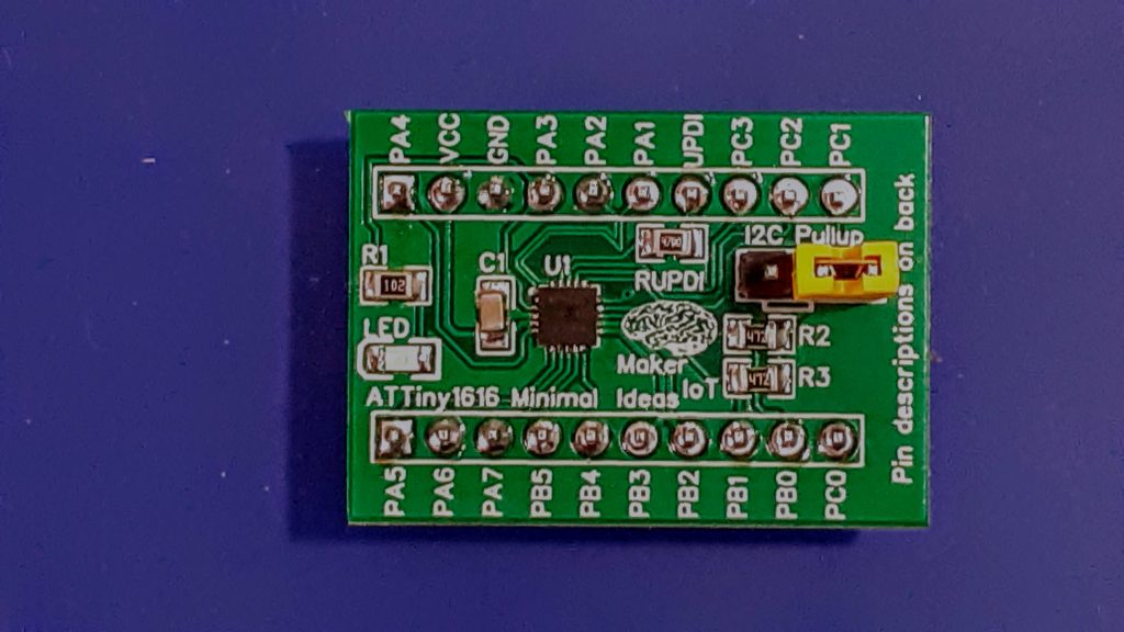
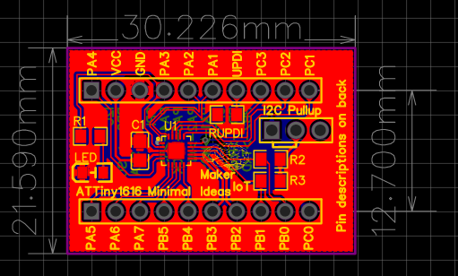
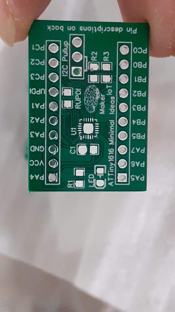
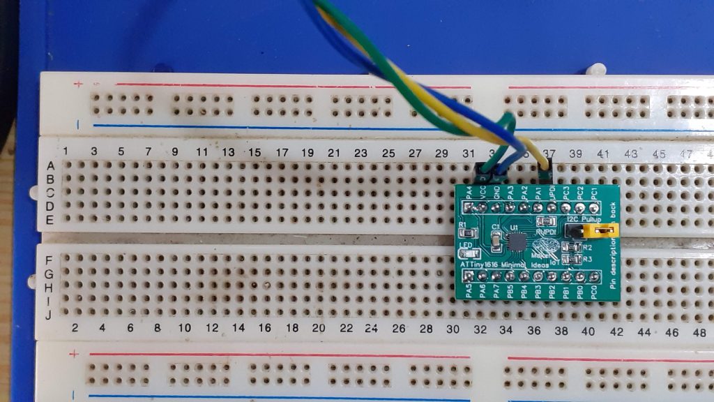
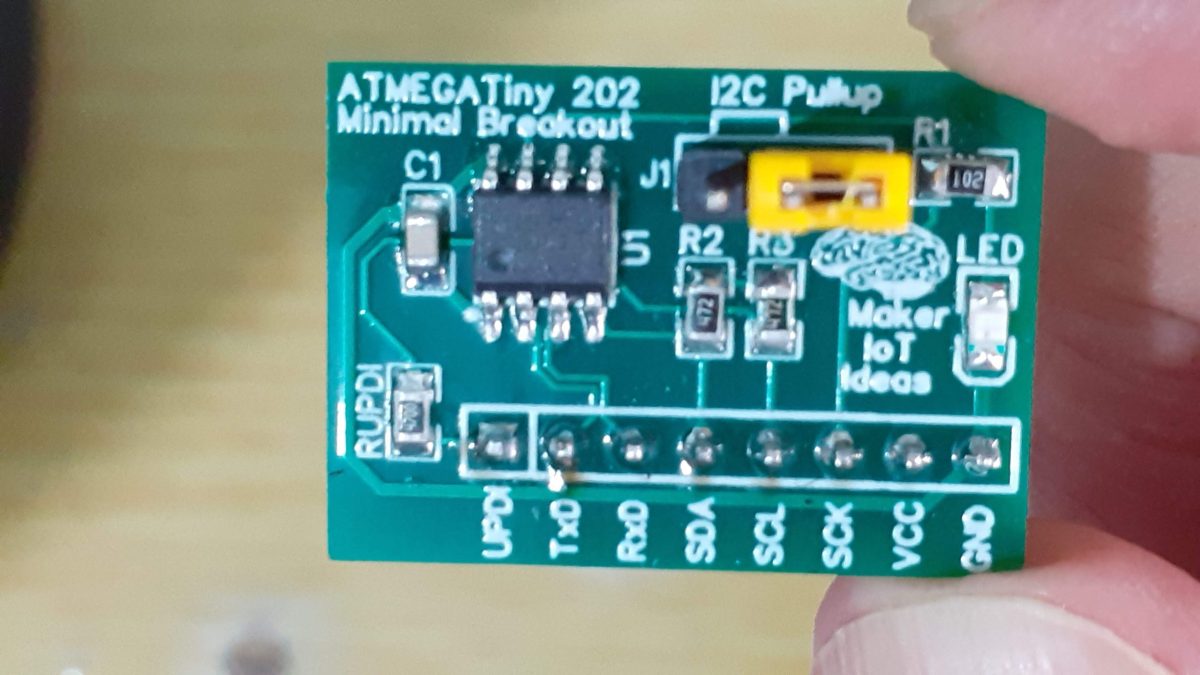
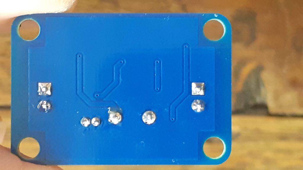
The PCB – Minimal working configuration – with a few extras
The PCB break-out all 18 of the GPIO pins, while it is only recommended to use 17 of them, unless, like in the case of the ATTiny202, you have access to an HV UPDI programmer. It also becomes possible, although still being quite tedious and awkward, to use the OptiBoot Bootloader on this chip, although it is still not quite recommended. Just using a UPDI programmer, with a separate USB-to-Serial adapter on another port is still definitely the easiest.
The Board contains an LED, on PIN_PA4, Arduino Pin 16, as well as onboard I2C pull-up resistors, selectable via a jumper. It is important to note that the current version DOES NOT contain a voltage regulator on the PCB. It is up to you to provide a regulated voltage source, in the range of 1.8v to 5.5v DC
It is recommended to clock the Chip at 16MHz when running at 5v ( 20Mhz is possible, But I did not bother to test that yet)
8Mhz when running at 3.3v
0-5Mhz when running at 1.8v
See the Datasheet, as well as the megaTinyCore documentation for exact details on this.
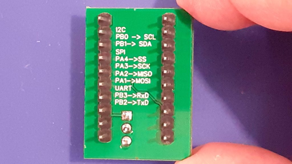
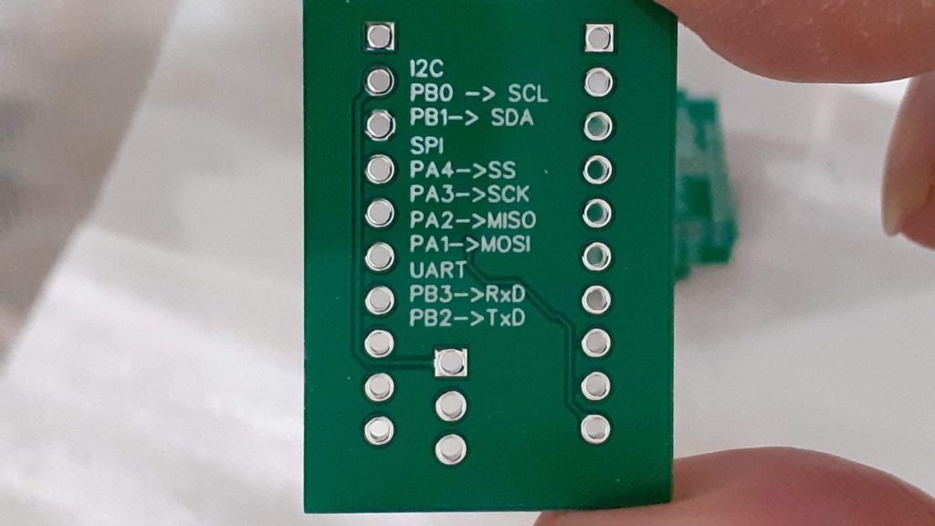
Commonly used peripherals, by myself, are listed on the back of the PCB for easy reference.
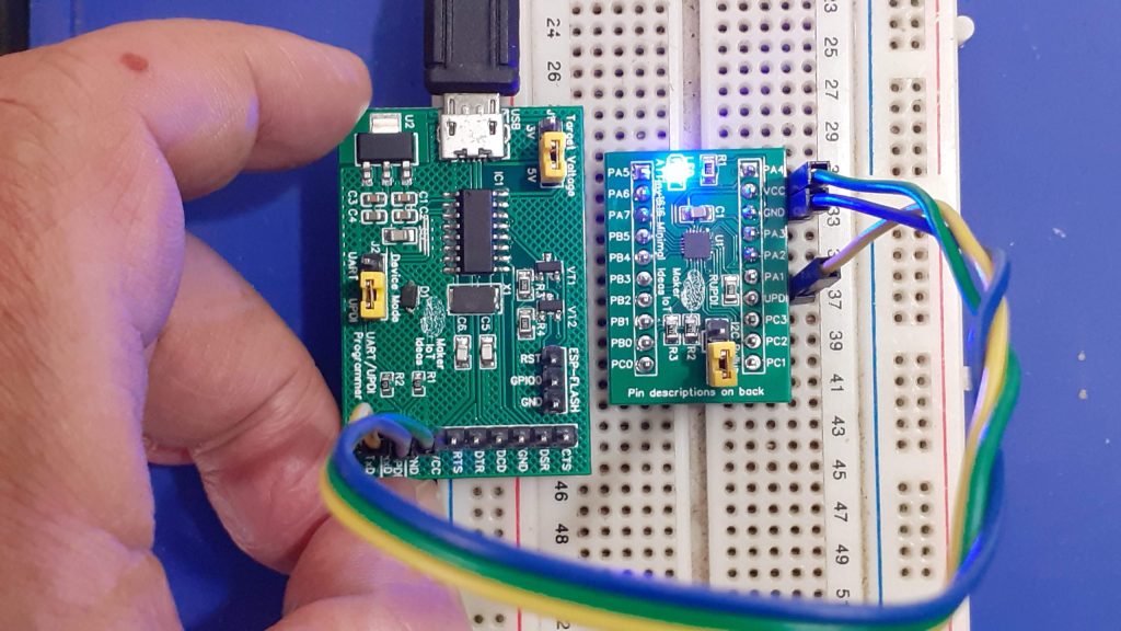
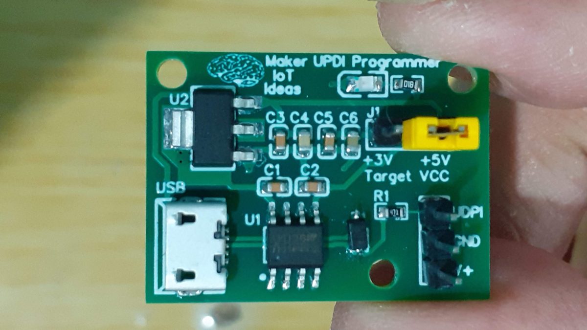
Programming the board
Programming is possible with Arduino IDE (and platformIO, ( I didn’t test that, as I find VS-Code tedious to use ), as well as MPLab from Microchip.
For the Arduino IDE, you have to install the megaTinyCore Arduino Core, as already mentioned above. ( This also apparently works for PlatformIO)
Full instructions, as well as some very useful other tips and information, is available in the core documentation, so do put in the effort to actually read the documentation. You won’t be sorry that you did.
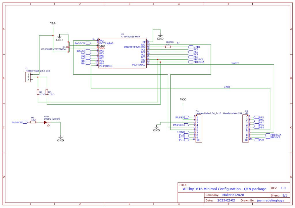
The Schematic
Design and Assembly
The board is designed as a double-layer PCB, with ground planes on both sides.
Due to the MCU package having a QFN footprint, using a proper SMD stencil is strongly recommended.
Hot-Air or a hotplate will also be quite useful to ensure success with this project. Passive components can be hand soldered though.
Manufacturing
I choose PCBWay for my PCB manufacturing. Why? What makes them different from the rest?
PCBWay‘s business goal is to be the most professional PCB manufacturer for prototyping and low-volume production work in the world. With more than a decade in the business, they are committed to meeting the needs of their customers from different industries in terms of quality, delivery, cost-effectiveness and any other demanding requests. As one of the most experienced PCB manufacturers and SMT Assemblers in China, they pride themselves to be our (the Makers) best business partners, as well as good friends in every aspect of our PCB manufacturing needs. They strive to make our R&D work easy and hassle-free.
How do they do that?
PCBWay is NOT a broker. That means that they do all manufacturing and assembly themselves, cutting out all the middlemen, and saving us money.
PCBWay’s online quoting system gives a very detailed and accurate picture of all costs upfront, including components and assembly costs. This saves a lot of time and hassle.
PCBWay gives you one-on-one customer support, that answers you in 5 minutes ( from the Website chat ) , or by email within a few hours ( from your personal account manager). Issues are really resolved very quickly, not that there are many anyway, but, as we are all human, it is nice to know that when a gremlin rears its head, you have someone to talk to that will do his/her best to resolve your issue as soon as possible.
Find out more here

Picture Gallery


