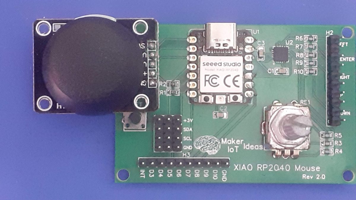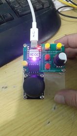

Over the last few months, We have been steadily improving the design of our XIAO RP2040-based mouse device. With this, ver 3.0 all the hardware bugs were finally eliminated, and we also placed the device into its first-ever enclosure.
Let us take a look at the design
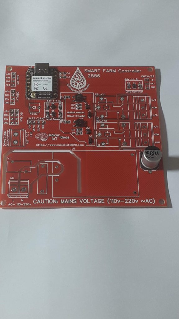
The PCB and Schematic

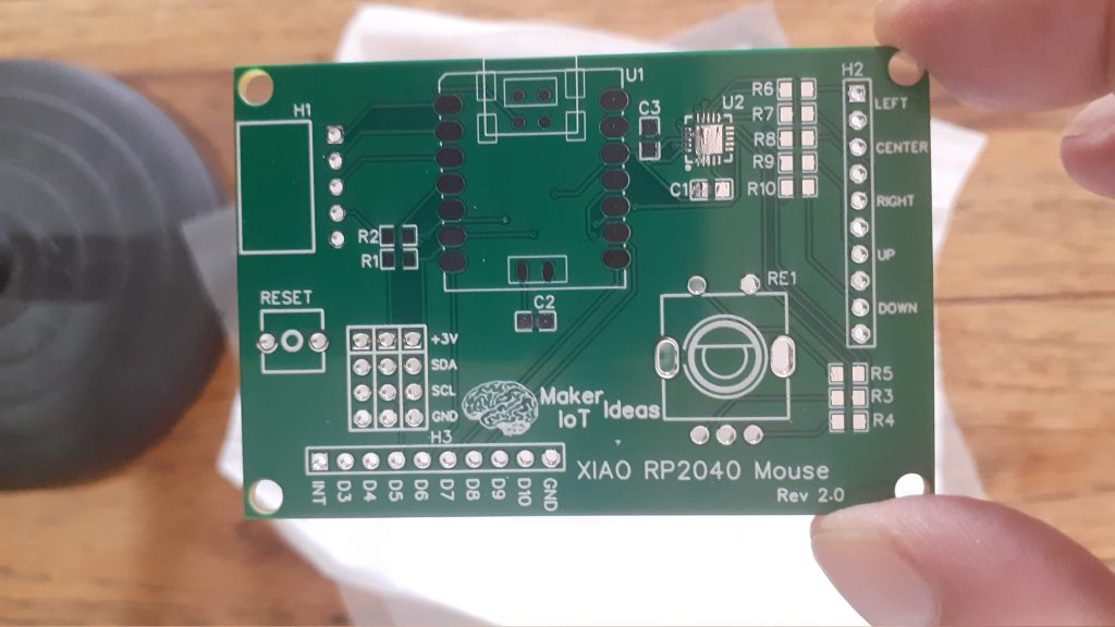
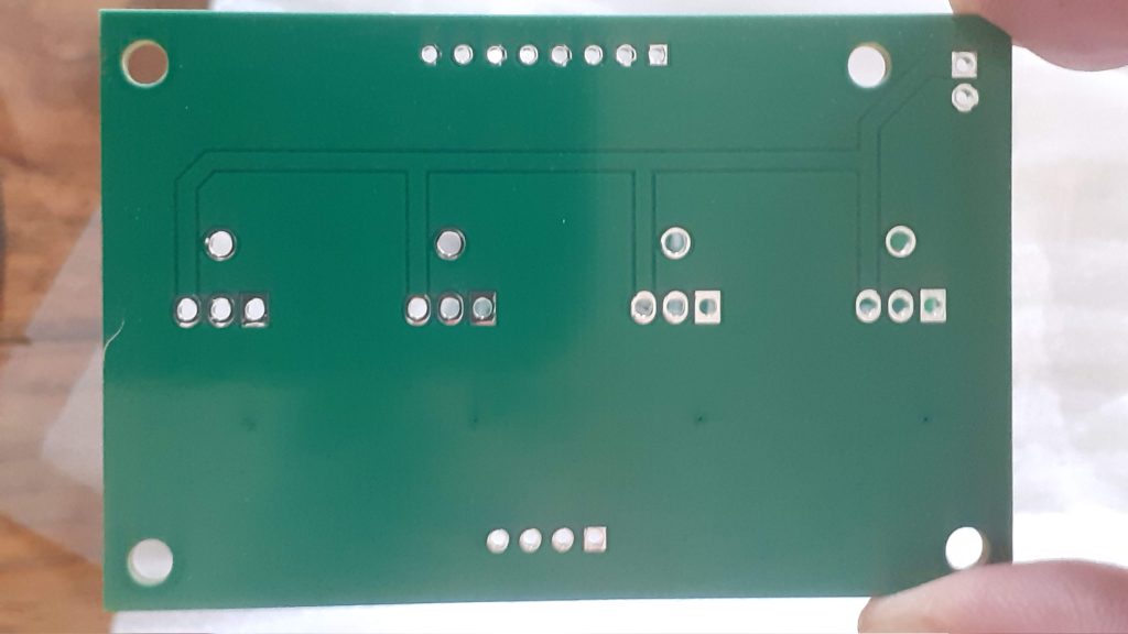
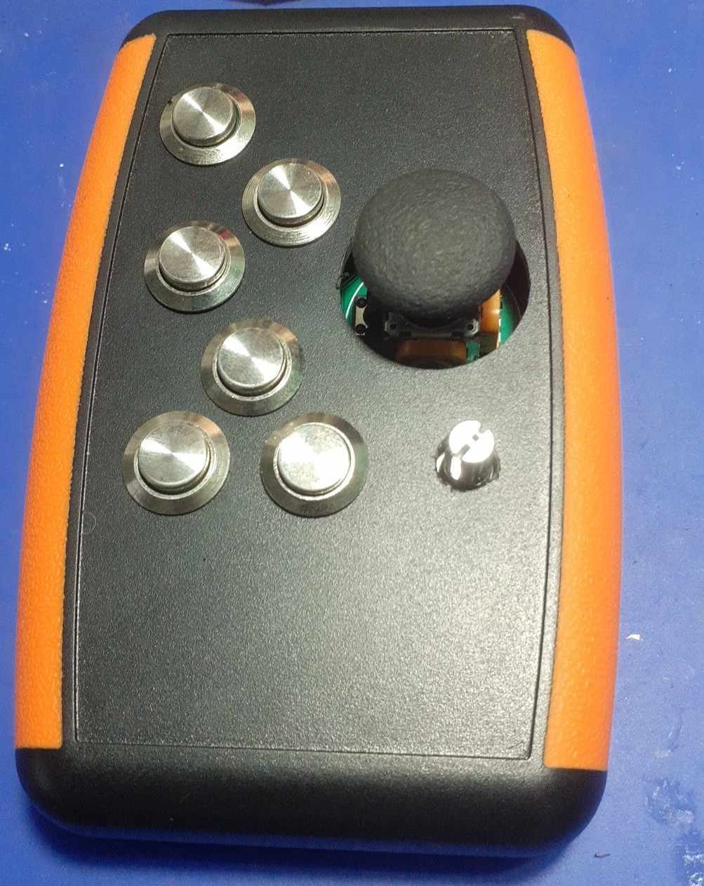
The PCB is a very strange shape, with lots of cut-outs. This is to accommodate the big push buttons that will be mounted in the enclosure, as well as to fit nicely into the mounting area of the enclosure… This design took quite some time with a pair of callipers and CAD, but all went well, and the shape is perfectly accurate.
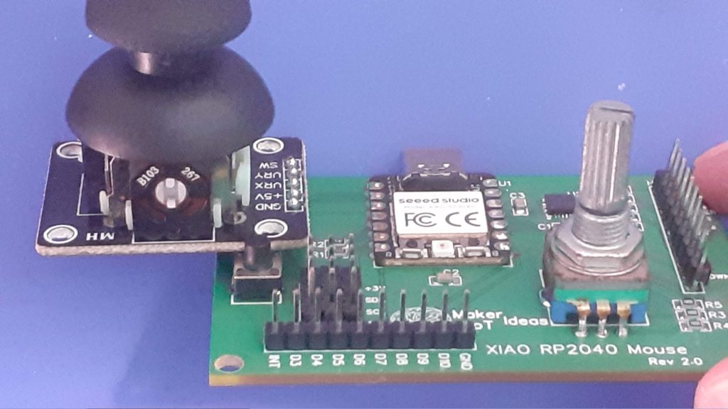
The schematic is also straight forward, with the only real changes begin to the rotary encoder. In ver 2.0, We connected the encoder to the MCP23008, but for some reason CircuitPython does not seem to like an encoder connected to an IO extender… That forced us to do some software hack to use the encoder… I have thus decided to change things around in ver 3.0 and move the encoder back to the native GPIO on the XIAO RP2040
It is also interesting to note that the circuit was initially designed for the XIAO ESP32S3, but due to issues with stock, as well as crazy prices on local parts, we made a quick turn-around and went back to the RP2040. The ESP32S3 was going to allow us to implement a wireless device, through using ESPNow protocol… That may still be done in future, but for now, I think we have done enough work on the mouse device for the time being…
Manufacturing the PCB and Assembly
I choose PCBWay for my PCB manufacturing. Why? What makes them different from the rest?
PCBWay‘s business goal is to be the most professional PCB manufacturer for prototyping and low-volume production work in the world. With more than a decade in the business, they are committed to meeting the needs of their customers from different industries in terms of quality, delivery, cost-effectiveness and any other demanding requests. As one of the most experienced PCB manufacturers and SMT Assemblers in China, they pride themselves to be our (the Makers) best business partners, as well as good friends in every aspect of our PCB manufacturing needs. They strive to make our R&D work easy and hassle-free.
How do they do that?
PCBWay is NOT a broker. That means that they do all manufacturing and assembly themselves, cutting out all the middlemen, and saving us money.
PCBWay’s online quoting system gives a very detailed and accurate picture of all costs upfront, including components and assembly costs. This saves a lot of time and hassle.
PCBWay gives you one-on-one customer support, that answers you in 5 minutes ( from the Website chat ), or by email within a few hours ( from your personal account manager). Issues are really resolved very quickly, not that there are many anyway, but, as we are all human, it is nice to know that when a gremlin rears its head, you have someone to talk to who will do his/her best to resolve your issue as soon as possible.
Find out more here

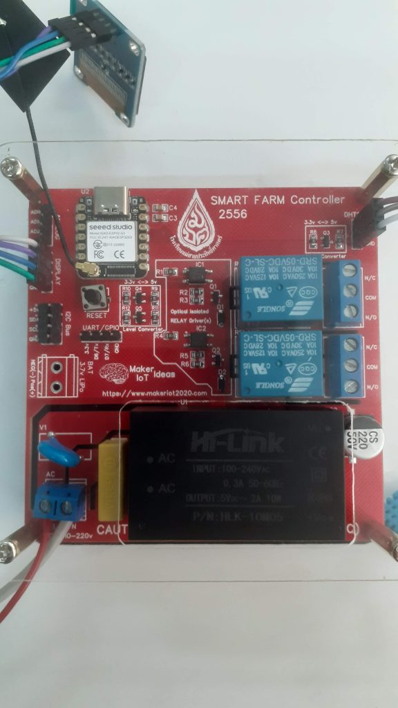
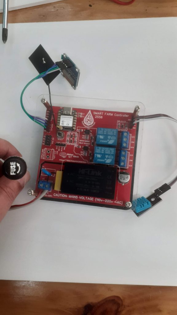
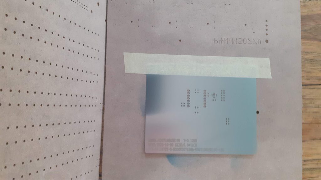
Assembly was quite easy, I chose to use a stencil, because the IO Expander chip has a very tiny footprint, as well as a leadless package… The stencil definitely helps prevent excessive solder paste, as well as saves a lot of time on reworking later…


In the picture above, we can clearly see why I had to design the PCB with such an irregular shape.
Firmware and Coding
We are still using CircuitPython for the firmware on this device. It is not perfect, but it works, well sort of anyway. What does that mean? Well… As far as the mouse functions are concerned, clicking, scrolling, moving the pointer – all of that is works perfectly, and thus allows me to use the device for basic operations every day. Drag and Drop, as well as selecting and or highlighting text DOES NOT work. This seem to be an issue with the HID code in Circuitpython, meaning it doesn’t seem to be implemented. It is also way beyond my abilities to implement it myself…
Below is the code.py file, with the boot.py below that
import time
import board
import busio
from rainbowio import colorwheel
import neopixel
import rotaryio
import microcontroller
from digitalio import Direction
from adafruit_mcp230xx.mcp23008 import MCP23008
import digitalio
i2c = busio.I2C(board.SCL, board.SDA)
mcp = MCP23008(i2c)


from analogio import AnalogIn
import usb_hid
from adafruit_hid.mouse import Mouse
joyX = board.A0
joyY = board.A1
JoyBtn = board.D2

LeftBtn = 0
CenterBtn = 1
RightBtn = 2
UpBtn = 3
DownBtn = 4
EncoderBtn = 5


mouse = Mouse(usb_hid.devices)
xAxis = AnalogIn(joyX)
yAxis = AnalogIn(joyY)

# NEOPIXEL
pixel_pin = board.NEOPIXEL
num_pixels = 1
pixels = neopixel.NeoPixel(pixel_pin, num_pixels, brightness=0.1, auto_write=False)

leftbutton = mcp.get_pin(LeftBtn)
leftbutton.direction = digitalio.Direction.INPUT
leftbutton.pull = digitalio.Pull.UP

centerbutton = mcp.get_pin(CenterBtn)
centerbutton.direction = digitalio.Direction.INPUT
centerbutton.pull = digitalio.Pull.UP

maint_btn = digitalio.DigitalInOut(JoyBtn)
maint_btn.switch_to_input(pull=digitalio.Pull.UP)

rightbutton = mcp.get_pin(RightBtn)
rightbutton.direction = digitalio.Direction.INPUT
rightbutton.pull = digitalio.Pull.UP

enc_btn = mcp.get_pin(EncoderBtn)
enc_btn.direction = digitalio.Direction.INPUT
enc_btn.pull = digitalio.Pull.UP

scroll_up = mcp.get_pin(UpBtn)
scroll_up.direction = digitalio.Direction.INPUT
scroll_up.pull = digitalio.Pull.UP

scroll_down = mcp.get_pin(DownBtn)
scroll_down.direction = digitalio.Direction.INPUT
scroll_down.pull = digitalio.Pull.UP


mousewheel = rotaryio.IncrementalEncoder(board.D6, board.D7, 4)
last_position = mousewheel.position
print(mousewheel.position)

move_speed = 3
enc_down = 0

RED = (255, 0, 0)
YELLOW = (255, 150, 0)
GREEN = (0, 255, 0)
CYAN = (0, 255, 255)
BLUE = (0, 0, 255)
PURPLE = (180, 0, 255)
BLACK = (0, 0, 0)


if move_speed == 0:
    in_min, in_max, out_min, out_max = (0, 65000, -20, 20)
    filter_joystick_deadzone = (
        lambda x: int((x - in_min) * (out_max - out_min) / (in_max - in_min) + out_min)
        if abs(x - 32768) > 500
        else 0
    )
if move_speed == 1:
    pixels.fill(GREEN)
    pixels.show()
    in_min, in_max, out_min, out_max = (0, 65000, -15, 15)
    filter_joystick_deadzone = (
        lambda x: int((x - in_min) * (out_max - out_min) / (in_max - in_min) + out_min)
        if abs(x - 32768) > 500
        else 0
    )
if move_speed == 2:
    pixels.fill(BLUE)
    pixels.show()
    in_min, in_max, out_min, out_max = (0, 65000, -10, 10)


filter_joystick_deadzone = (
        lambda x: int((x - in_min) * (out_max - out_min) / (in_max - in_min) + out_min)
        if abs(x - 32768) > 500
        else 0
    )
if move_speed == 3:
    pixels.fill(PURPLE)
    pixels.show()
    in_min, in_max, out_min, out_max = (0, 65000, -8, 8)
    filter_joystick_deadzone = (
        lambda x: int((x - in_min) * (out_max - out_min) / (in_max - in_min) + out_min)
        if abs(x - 32768) > 500
        else 0
    )
if move_speed == 4:
    pixels.fill(CYAN)
    pixels.show()
    in_min, in_max, out_min, out_max = (0, 65000, -5, 5)
    filter_joystick_deadzone = (
        lambda x: int((x - in_min) * (out_max - out_min) / (in_max - in_min) + out_min)
        if abs(x - 32768) > 500
        else 0
    )


pixels.fill(BLACK)
pixels.show()
while True:
    # Set mouse accelleration ( speed)
    #print(mousewheel.position)
    if move_speed == 0:
        pixels.fill(BLACK)
        pixels.show()
        in_min, in_max, out_min, out_max = (0, 65000, -20, 20)
        filter_joystick_deadzone = (
            lambda x: int(
                (x - in_min) * (out_max - out_min) / (in_max - in_min) + out_min
            )
            if abs(x - 32768) > 500
            else 0
        )
    if move_speed == 1:
        pixels.fill(GREEN)
        pixels.show()
        in_min, in_max, out_min, out_max = (0, 65000, -15, 15)
        filter_joystick_deadzone = (
            lambda x: int(
                (x - in_min) * (out_max - out_min) / (in_max - in_min) + out_min
            )
            if abs(x - 32768) > 500
            else 0
        )
    if move_speed == 2:
        pixels.fill(BLUE)
        pixels.show()
        in_min, in_max, out_min, out_max = (0, 65000, -10, 10)
        filter_joystick_deadzone = (
            lambda x: int(
                (x - in_min) * (out_max - out_min) / (in_max - in_min) + out_min
            )
            if abs(x - 32768) > 500
            else 0
        )
    if move_speed == 3:
        pixels.fill(PURPLE)
        pixels.show()
        in_min, in_max, out_min, out_max = (0, 65000, -8, 8)
        filter_joystick_deadzone = (
            lambda x: int(
                (x - in_min) * (out_max - out_min) / (in_max - in_min) + out_min
            )
            if abs(x - 32768) > 500
            else 0
        )
    if move_speed == 4:
        pixels.fill(CYAN)
        pixels.show()
        in_min, in_max, out_min, out_max = (0, 65000, -5, 5)
        filter_joystick_deadzone = (
            lambda x: int(
                (x - in_min) * (out_max - out_min) / (in_max - in_min) + out_min
            )
            if abs(x - 32768) > 500
            else 0
        )

    current_position = mousewheel.position
    position_change = current_position - last_position

    x_offset = filter_joystick_deadzone(xAxis.value) * -1  # Invert axis
    y_offset = filter_joystick_deadzone(yAxis.value)
    mouse.move(x_offset, y_offset, 0)

    if enc_btn.value and enc_down == 1:
        move_speed = move_speed + 1
        if move_speed > 4:
            move_speed = 0

        # print (move_speed)
        enc_down = 0

    if not enc_btn.value:
        enc_down = 1

    if leftbutton.value:
        mouse.release(Mouse.LEFT_BUTTON)
        # pixels.fill(BLACK)
        # pixels.show()
    else:
        mouse.press(Mouse.LEFT_BUTTON)
        pixels.fill(GREEN)
        pixels.show()

    if centerbutton.value:
        mouse.release(Mouse.MIDDLE_BUTTON)
    else:
        mouse.press(Mouse.MIDDLE_BUTTON)
        pixels.fill(YELLOW)
        pixels.show()

    # Center button on joystick
    if maint_btn.value:
        mouse.release(Mouse.LEFT_BUTTON)
    else:
        mouse.press(Mouse.LEFT_BUTTON)
        pixels.fill(GREEN)
        pixels.show()

    if rightbutton.value:
        mouse.release(Mouse.RIGHT_BUTTON)
        # pixels.fill(BLACK)
        # pixels.show()
    else:
        mouse.press(Mouse.RIGHT_BUTTON)
        pixels.fill(PURPLE)
        pixels.show()

    if not scroll_up.value:
        mouse.move(wheel=1)
        time.sleep(0.25)
        pixels.fill(BLUE)
        pixels.show()

    if not scroll_down.value:
        mouse.move(wheel=-1)
        time.sleep(0.25)
        pixels.fill(CYAN)
        pixels.show()

    if not scroll_up.value and not scroll_down.value:
        for x in range(4):
            pixels.fill(RED)
            pixels.show()
            time.sleep(0.5)
            pixels.fill(BLACK)
            pixels.show()
            time.sleep(0.5)
        microcontroller.reset()


    if position_change > 0:
        mouse.move(wheel=position_change)
        #print(current_position)
        #pixels.fill(BLUE)
        #pixels.show()
    elif position_change < 0:
        mouse.move(wheel=position_change)
        #print(current_position)
        #pixels.fill(CYAN)
        #pixels.show()
    last_position = current_position
    pixels.fill(BLACK)
    pixels.show()
boot.py
import storage
import board, digitalio
import time
from rainbowio import colorwheel
import neopixel
import busio
from digitalio import Direction
from adafruit_mcp230xx.mcp23008 import MCP23008
import digitalio
i2c = busio.I2C(board.SCL, board.SDA)
mcp = MCP23008(i2c)


#button = digitalio.DigitalInOut(board.D8)
#button.pull = digitalio.Pull.UP

button = mcp.get_pin(6)
button.direction = digitalio.Direction.INPUT
button.pull = digitalio.Pull.UP

Rstbutton = mcp.get_pin(7)
Rstbutton.direction = digitalio.Direction.INPUT
Rstbutton.pull = digitalio.Pull.UP

# NEOPIXEL
pixel_pin = board.NEOPIXEL
num_pixels = 1
pixels = neopixel.NeoPixel(pixel_pin,num_pixels,brightness=0.2,auto_write=False)

RED = (255, 0, 0)
YELLOW = (255,150, 0)
GREEN = (0, 255, 0)
CYAN = (0, 255, 255)
BLUE = (0, 0, 255)
PURPLE = (180, 0, 255)
BLACK = (0, 0, 0)

# Disable devices only if button is not pressed.
#usb_hid.enable((), boot_device=2)
if button.value:
   pixels.fill(GREEN)
   pixels.show()
   storage.disable_usb_drive()
   usb_cdc.disable()
else:
    pixels.fill(RED)
    pixels.show()
    usb_cdc.enable(console=True, data=False)
    storage.enable_usb_drive()


time.sleep(5)
# Write your code here :-)